

查询STD2NK60Z供应商
STF2NK60Z - STQ2NK60ZR-AP
STP2NK60Z - STD2NK60Z-1
N-CHANNEL 600V - 7.2 Ω - 1.4A T O-220/TO- 220FP/ TO-92/IP AK
Zener-Protected SuperMESH™ MOSFET
Table 1: General Features
TYPE V
STF2NK60Z
STQ2NK60ZR-AP
STP2NK60Z
STD2NK60Z-1
■ TYPICAL R
■ EXTREMELY HIGH dv /d t CAPABILITY
■ ESD IMPROVED CAPABILITY
■ 100% AVALANCHE TESTED
■ NEW HIGH VOLTAGE BENCHMARK
■ GATE CHARGE MINIMIZED
DS
DSSRDS(on)ID
600 V
600 V
600 V
600 V
(on) = 7.2 Ω
< 8 Ω
< 8 Ω
< 8 Ω
< 8 Ω
1.4 A
0.4 A
1.4 A
1.4 A
Pw
20
3 W
45 W
45 W
DESCRIPTION
The SuperMESH™ series is obtained through an
extreme optimization of ST’s well established
strip-based PowerMESH™ layout. In addition to
pushing on-resistance significantly down, special
care is taken to ensure a very good dv/dt capability
for the most demanding applications. Such series
complements ST full range of high voltage MOSFET s including revolutionary MDmesh™ products.
APPLICATIONS
■ LOW POWER BATTERY CHARGERS
■ SWITH MODE LOW POWER
SUPPLIES(SMPS)
■ LOW POWER, BALLAST, CFL (COMPACT
FLUORESCENT LAMPS)
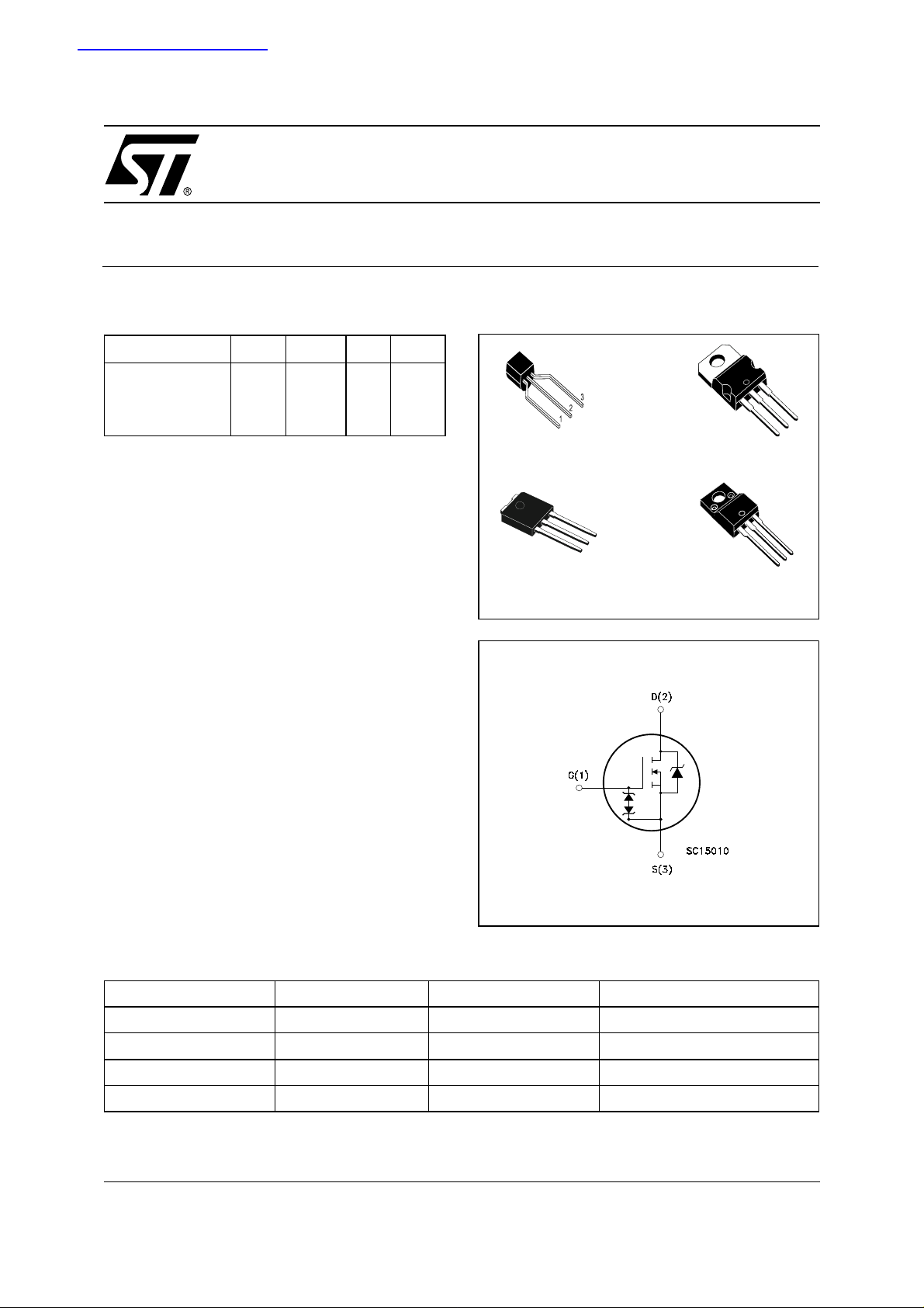
Figure 1: Package
TO-92 (Ammopack)
TO-220
3
2
1
IPAK
TO-220FP
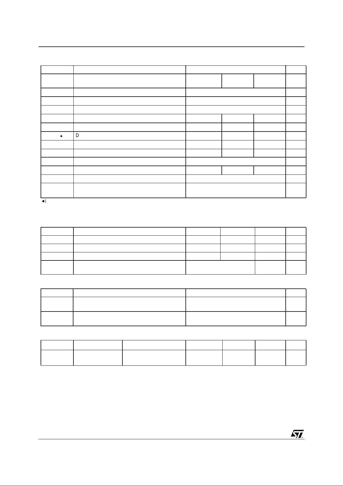
Figure 2: Internal Schematic Diagram
3
2
1
3
2
1
Table 2: Order Codes
Part Number Marking Package Packaging
STQ2NK60ZR-AP Q2NK60ZR TO-92 AMMOPAK
STP2NK60Z P2NK60Z TO-220 TUBE
STD2NK60Z-1 D2NK60Z IPAK TUBE
STF2NK60Z F2NK60Z TO-220FP TUBE
Rev. 5
1/16September 2005
STQ2NK60ZR-AP - STP2NK60Z - STF2NK60Z - STD2NK60Z-1
Table 3: Absolute Maximum ratings
Symbol Parameter Value Unit
TO-220 /
IPAK
V
I
V
V
DM
P
DS
DGR
GS
I
D
I
D
TOT
Drain-source Voltage (VGS = 0)
Drain-gate Voltage (RGS = 20 kΩ)
Gate- source Voltage ± 30 V
Drain Current (continuous) at TC = 25°C
Drain Current (continuous) at TC = 100°C
()
Drain Current (pulsed) 5.6 1.6 5.6 (*) A
Total Dissipation at TC = 25°C
1.4 0.4 1.4 (*) A
0.77 0.25 0.77 (*) A
45 3 20 W
Derating Factor 0.36 0.025 0.16 W/°C
V
ESD(G-S)
V
ISO
Gate source ESD (HBM-C= 100pF, R=1.5kΩ) 1500 V
Insulation Withstand Voltage (DC) 2500 V
dv/dt (1) Peak Diode Recovery voltage slope 4.5 V/ns
T
j
T
stg
() Pulse wi dt h l i m i ted by safe operating area
≤ 1.4A, di/dt ≤ 200A/µs, VDD ≤ V
(1) I
SD
(*) Limit ed only by maxi m um temperature allowed
Operating Junction Temperature
Storage Temperature
, Tj ≤ T
(BR)DSS
JMAX.
TO-92 TO-220FP
600 V
600 V
-55 to 150 °C
Table 4: Thermal Data
TO-220/IPAK TO-220FP TO-92 Unit
Rthj-case Thermal Resistance Junction-case Max 2.77 6.25 -- °C/W
Rthj-amb Thermal Resistance Junction-ambient Max 100 100 120 °C/W
Rthj-lead Thermal Resistance Junction-lead Max -- -- 40 °C/W
T
l
Maximum Lead Temperature For Soldering
300 260 °C
Purpose
Table 5: Avalanche Characteristics
Symbol Parameter Max Value Unit
I
AR
E
AS
Avalanche Current, Repetitive or Not-Repetitive
(pulse width limited by T
max)
j
Single Pulse Avalanche Energy
(starting T
= 25 °C, ID = IAR, VDD = 50 V)
j
1.4 A
90 mJ
Table 6: Gate-Source Zener Diode
Symbol Parameter Test Conditions Min. Typ. Max. Unit
BV
GSO
Gate source
Igs= ± 1 mA (Open Drain) 30 V
Breakdown Voltage
PROTECTION FEATURES OF GATE-TO-SOURCE ZENER DIODES
The built-in back-to-back Zener diodes have sp ecifically been desig ned to enhance not only the dev ice’s
ESD capability, but also to make them safely absorb possible voltage transients that may occasionally be
applied from gate to source. In this respect the Zener voltage is appropriate to achieve an ef ficient and
cost-effective intervention to prot ect the device’s integrity. Thes e integrate d Z ener diodes thus avoid t he
usage of external components.
2/16
STQ2NK60ZR-AP - STP2NK 60Z - STF2NK60Z - STD2NK60Z-1
ELECTRICAL CHARACTERISTICS (T
=25°C UNLESS OTHERWISE SPECIFIED)
CASE
Table 7: On/Off
Symbol Parameter Test Conditions Min. Typ. Max. Unit
V
(BR)DSS
Drain-source
ID = 1mA, VGS = 0 600 V
Breakdown Voltage
I
I
V
GS(th)
R
DS(on)
DSS
GSS
Zero Gate Voltage
Drain Current (V
GS
= 0)
Gate-body Leaka ge
Current (V
DS
= 0)
Gate Threshold Voltage
Static Drain-source On
= Max Rating
V
DS
V
= Max Rating, TC = 125 °C
DS
V
= ± 20V ±10 µA
GS
V
= VGS, ID = 50 µA
DS
33.754.5V
1
50
VGS = 10V, ID = 0.7 A 7.2 8 Ω
Resistance
Table 8: Dynamic
Symbol Parameter Test Conditions Min. Typ. Max. Unit
g
C
oss eq.
fs
C
C
C
t
d(on)
t
d(off)
Q
Q
Q
iss
oss
rss
t
r
t
r
gs
gd
(1)
g
Forward Transconductance
Input Capacitance
Output Capacitance
Reverse Transfer Capacitance
(3)
Equivalent Outpu t Capacitance
Turn-on Delay Time
Rise Ti me
Turn-off Delay Time
Fall Time
Total Gate Charge
Gate-Source Charge
Gate-Drain Charge
VDS = 15 V, ID= 0.7 A 1 S
VDS = 25V, f = 1 MHz, VGS = 0 170
27
5
VGS = 0V, VDS = 0V to 480V 30
= 300 V, ID = 0.65 A,
V
DD
RG= 4.7 Ω, VGS = 10 V
(Resistive Load see, Figure
22)
= 480V, ID = 1.5 A,
V
DD
VGS = 10V
(see, Figure 24)
8
30
22
55
7.7
1.7
4
10
µA
µA
pF
pF
pF
pF
ns
ns
ns
ns
nC
nC
nC
Table 9: Source Drain Diode
Symbol Parameter Test Conditions Min. Typ. Max. Unit
I
SD
I
(2)
SDM
(1)
V
SD
t
rr
Q
rr
I
RRM
t
rr
Q
rr
I
RRM
(1) Pulsed: Pulse du rat i on = 300 µs, du ty cycle 1.5 % .
(2) Pulse width limited by safe operating area.
(3) C
oss eq.
Source-drain Current
Source-drain Current (pulsed)
Forward On Voltage
Reverse Recovery Time
Reverse Recovery Charge
Reverse Recovery Current
Reverse Recovery Time
Reverse Recovery Charge
Reverse Recovery Current
is defined as a constant equivalent capacitance giving the same charging time as Coss when VDS increases from 0 to 80% VDSS
ISD = 1.5 A, VGS = 0
= 1.3 A, di/dt = 100 A/µs
I
SD
VDD = 25V, Tj = 25°C
(see test circuit, Figure 23)
= 1.3 A, di/dt = 100 A/µs
I
SD
V
= 25V, Tj = 150°C
DD
(see test circuit, Figure 23)
250
550
4.4
300
690
4.6
1.5
6
1.6 V
A
A
ns
µC
A
ns
µC
A
3/16
STQ2NK60ZR-AP - STP2NK60Z - STF2NK60Z - STD2NK60Z-1
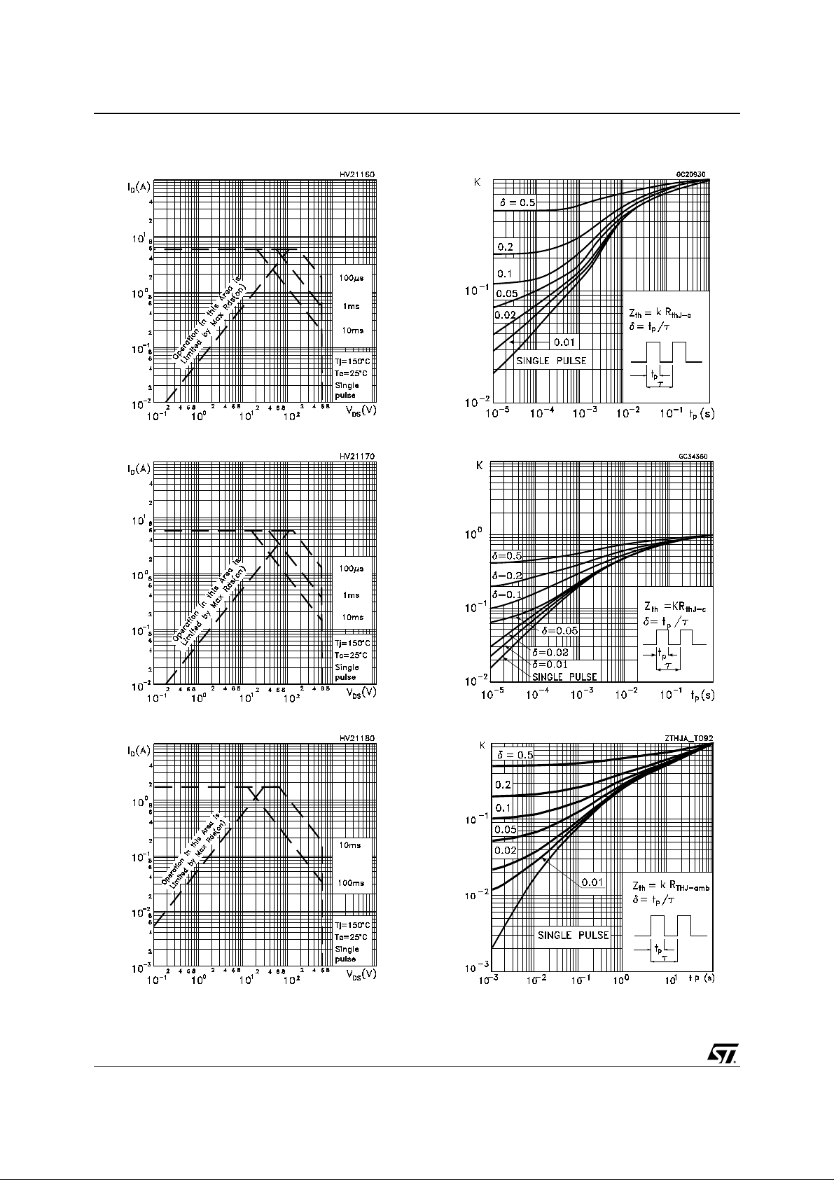
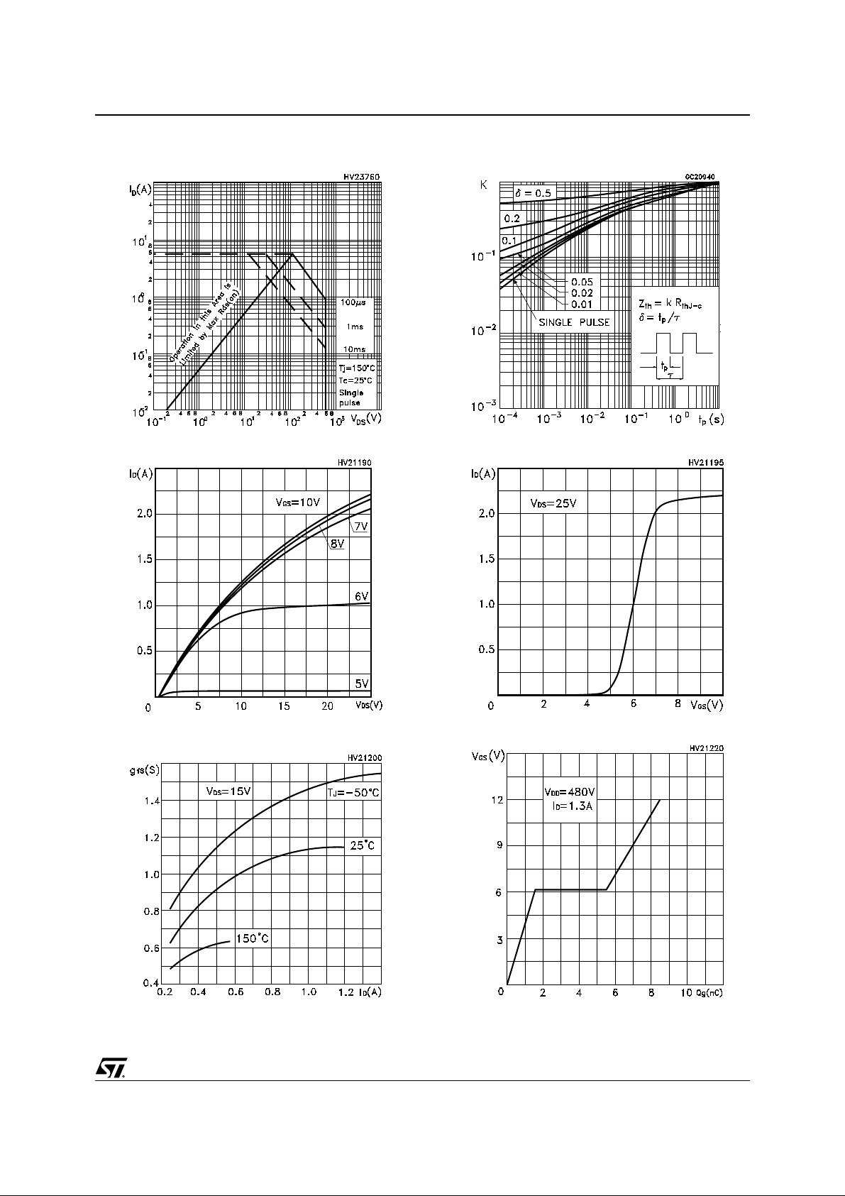
Figure 3: .Safe Operating Area For TO-220
Figure 4: Safe Operating Area For IPAK
Figure 6: Thermal Impedance For TO-220
Figure 7: Thermal Impedance For IPAK
Figure 5: Safe Operating Area For TO-92
4/16
Figure 8: Thermal Impedance For TO-92
STQ2NK60ZR-AP - STP2NK 60Z - STF2NK60Z - STD2NK60Z-1
Figure 9: Safe Operating Area For TO-220FP
Figure 10: Output Characteristics
Figure 12: Thermal Impedan ce Fo r TO-220 FP
Figure 13: Transfer Characteristics
Figure 11: Transconductance
Figure 14: Gate Charge vs Gate-source Voltage
5/16

STQ2NK60ZR-AP - STP2NK60Z - STF2NK60Z - STD2NK60Z-1
Figure 15: Static Drain-source On Resistance
Figure 16: Capacitance Variations
Figure 18: Source-Drain Forwa rd Characteristics
Figure 19: Maximum Avalanche Energy vs
Temperature
Figure 17: Normalized Gate Thereshold Voltage vs Temperature
6/16
Figure 20: Normalized On Resistance vs Temperature

STQ2NK60ZR-AP - STP2NK 60Z - STF2NK60Z - STD2NK60Z-1
Figure 21: Normalized BV
vs Temperature
DSS
7/16
STQ2NK60ZR-AP - STP2NK60Z - STF2NK60Z - STD2NK60Z-1
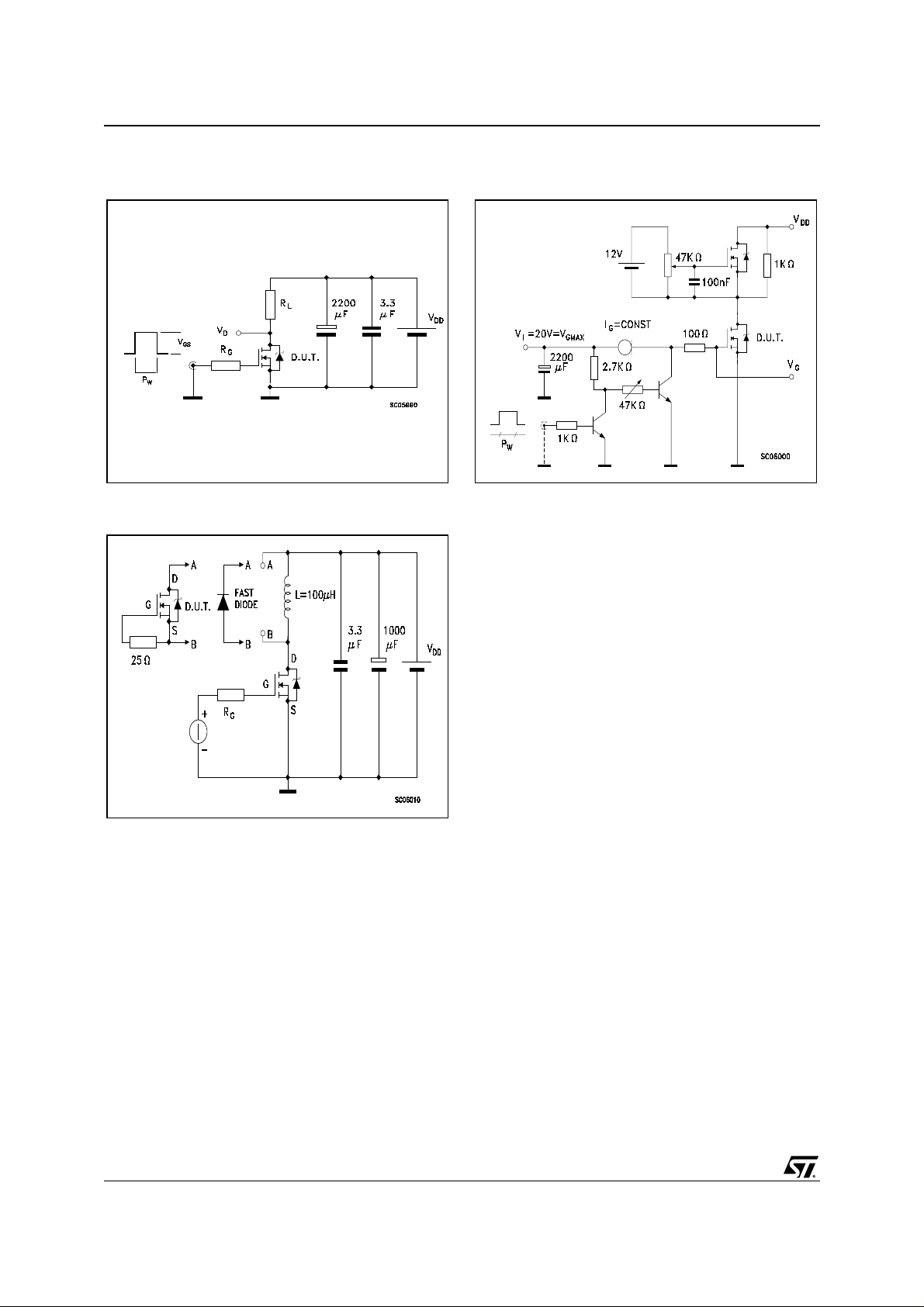
Figure 22: Switching Times Test Circuit For
Resistive Load
Figure 23: Test Circuit For Inductive Load
Switching and Diode Recovery Times
Figure 24: Gate Charge Test Circuit
8/16

STQ2NK60ZR-AP - STP2NK 60Z - STF2NK60Z - STD2NK60Z-1
In order to meet environmental requirements, ST offers these devices in ECOPACK® packages. These
packages have a Lead-free second level interconnect . The category of second level interconnect is
marked on the package and on the inner box label, i n compliance with JEDEC Standard JESD97. The
maximum ratings related to soldering conditions are also marked on the inner box label. ECOPACK is an
ST trademark. ECOPACK specifications are available at: www.st.com
9/16

STQ2NK60ZR-AP - STP2NK60Z - STF2NK60Z - STD2NK60Z-1
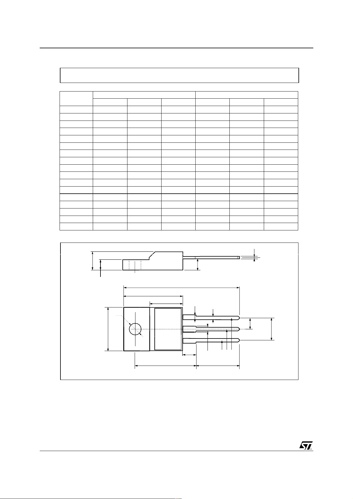
TO-220 MECHANICAL DATA
DIM.
A 4.40 4.60 0.173 0.181
b 0.61 0.88 0.024 0.034
b1 1.15 1.70 0.045 0.066
c 0.49 0.70 0.019 0.027
D 15.25 15.75 0.60 0.620
E 10 10.40 0.393 0.409
e 2.40 2.70 0.094 0.106
e1 4.95 5.15 0.194 0.202
F 1.23 1.32 0.048 0.052
H1 6.20 6.60 0.244 0.256
J1 2.40 2.72 0.094 0.107
L 13 14 0.511 0.551
L1 3.50 3.93 0.137 0.154
L20 16.40 0.645
L30 28.90 1.137
øP 3.75 3.85 0.147 0.151
Q 2.65 2.95 0.104 0.116
MIN. TYP MAX. MIN. TYP. MAX.
mm. inch
10/16

STQ2NK60ZR-AP - STP2NK 60Z - STF2NK60Z - STD2NK60Z-1
TO-92 AMMOPACK
DIM.
A1 4.45 4.95 0.170 0.194
T 3.30 3.94 0.130 0.155
T1 1.6 0.06
T2 2.3 0.09
d 0.41 0.56 0.016 0.022
P0 12.5 12.7 12.9 0.49 0.5 0.51
P2 5.65 6.35 7.05 0.22 0.25 0.27
F1, F2 2.44 2.54 2.94 0.09 0.1 0.11
delta H -2 2 -0.08 0.08
W 17.5 18 19 0.69 0.71 0.74
W0 5.7 6 6.3 0.22 0.23 0.24
W1 8.5 9 9.25 0.33 0.35 0.36
W2 0.5 0.02
H 18.5 20.5 0.72 0.80
H0 15.5 16 16.5 0.61 0.63 0.65
H1 25 0.98
D0 3.8 4 4.2 0.15 0.157 0.16
t 0.9 0.035
L110.43
l1 3 0.11
delta P -1 1 -0.04 0.04
MIN. TYP MAX. MIN. TYP. MAX.
mm. inch
11/16

STQ2NK60ZR-AP - STP2NK60Z - STF2NK60Z - STD2NK60Z-1
0068771-E
TO-251 (IPAK) MECHANICAL DATA
DIM.
MIN. TYP. MAX. MIN. TYP. MAX.
mm inch
A 2.2 2.4 0.086 0.094
A1 0.9 1.1 0.035 0.043
A3 0.7 1.3 0.027 0.051
B 0.64 0.9 0.025 0.031
B2 5.2 5.4 0.204 0.212
B3 0.85 0.033
B5 0.3 0.012
B6 0.95 0.037
C 0.45 0.6 0.017 0.023
C2 0.48 0.6 0.019 0.023
D 6 6.2 0.236 0.244
E 6.4 6.6 0.252 0.260
G 4.4 4.6 0.173 0.181
H 15.9 16.3 0.626 0.641
L 9 9.4 0.354 0.370
L1 0.8 1.2 0.031 0.047
L2 0.8 1 0.031 0.039
H
C
A
12/16
E
= =
C2
L2
B2
= =
D
B3
2
1 3
L1
B6
A1
L
A3
B
B5
G
= =

STQ2NK60ZR-AP - STP2NK 60Z - STF2NK60Z - STD2NK60Z-1
TO-92 MECHANICAL DATA
DIM.
A 4.32 4.95 0.170 0.194
b 0.36 0.51 0.014 0.020
D 4.45 4.95 0.175 0.194
E 3.30 3.94 0.130 0.155
e 2.41 2.67 0.094 0.105
e1 1.14 1.40 0.044 0.055
L 12.70 15.49 0.50 0.610
R 2.16 2.41 0.085 0.094
S1 0.92 1.52 0.036 0.060
W 0.41 0.56 0.016 0.022
V5° 5°
MIN. TYP MAX. MIN. TYP. MAX.
mm. inch
13/16
STQ2NK60ZR-AP - STP2NK60Z - STF2NK60Z - STD2NK60Z-1
TO-220FP MECHANICAL DATA
DIM.
A 4.4 4.6 0.173 0.181
B 2.5 2.7 0.098 0.106
D 2.5 2.75 0.098 0.108
E 0.45 0.7 0.017 0.027
F 0.75 1 0.030 0.039
F1 1.15 1.7 0.045 0.067
F2 1.15 1.7 0.045 0.067
G 4.95 5.2 0.195 0.204
G1 2.4 2.7 0.094 0.106
H 10 10.4 0.393 0.409
L2 16 0.630
L3 28.6 30.6 1.126 1.204
L4 9.8 10.6 .0385 0.417
L5 2.9 3.6 0.114 0.141
L6 15.9 16.4 0.626 0.645
L7 9 9.3 0.354 0.366
Ø 3 3.2 0.118 0.126
MIN. TYP MAX. MIN. TYP. MAX.
mm. inch
E
A
D
B
14/16
L3
L6
L7
F1
F
G1
H
F2
123
L4
L2
L5
G

STQ2NK60ZR-AP - STP2NK 60Z - STF2NK60Z - STD2NK60Z-1
Table 10: Revision History
Date Revision Description of Change s
07-Jul-2004 3 The document chang e from “TARGET” to “COMPLETE”
New stylesheet
11/Nov/2004 4 Added TO-220FP
05-Sep-2005 5 Inserted Ecopack indication
15/16

STQ2NK60ZR-AP - STP2NK60Z - STF2NK60Z - STD2NK60Z-1
Information furnished is believed to be accurate and reliable. However, STMicroelectronics assumes no responsibility for the consequences
of use of such information nor for any infringement of patents or other rights of third parties which may result from its use. No license is gra nted
by implic ati o n or ot h er wis e und er an y pat ent or pa te nt r igh ts of STMi cr oe l ect ro ni cs . Sp ec if i cat i on s ment i o ned i n th is p ub li c ati on ar e s ubj ec t
to change without not ice. This publication supersedes and replaces all information previously sup plied. STMicroelectr onics products are not
authorized for use as critical components in life support devices or systems without express written approval of STMicroelectronics.
The ST logo is a registered trademark of STMicroelectronics
All other names are the property of their respective owners
© 2005 STMicroelectronics - All Rights Reserved
STMicroelectronics group of companies
Australia - Belgium - Brazil - Canada - China - Czech Republic - Finland - France - Germany - Hong Kong - India - Israel - Italy - Japan -
Malaysia - Malta - Morocco - Singapore - Spain - Sweden - Switzerland - United Kingdom - United States of America
16/16
 Loading...