

ST STPSC6H065 User Manual
Features
STPSC6H065
650 V power Schottky silicon carbide diode
Datasheet − production data
■ No or negligible reverse recovery
■ Switching behavior independent of
temperature
■ Dedicated to PFC applications
■ High forward surge capability
Description
The SiC diode is an ultrahigh performance power
Schottky diode. It is manufactured using a silicon
carbide substrate. The wide bandgap material
allows the design of a Schottky diode structure
with a 650 V rating. Due to the Schottky
construction, no recovery is shown at turn-off and
ringing patterns are negligible. The minimal
capacitive turn-off behavior is independent of
temperature.
Especially suited for use in PFC applications, this
ST SiC diode will boost the performance in hard
switching conditions. Its high forward surge
capability ensures more margin during transient
phases.
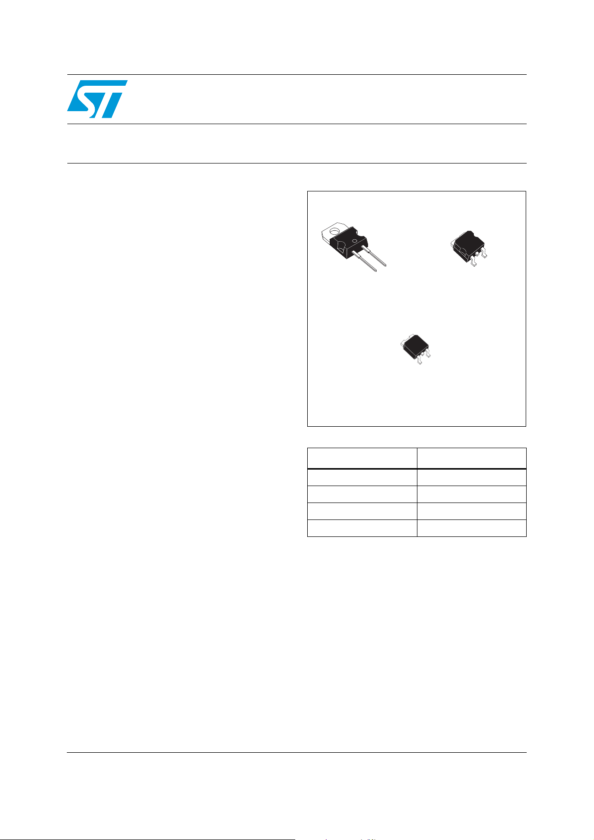
K
A
K
TO-220AC
STPSC6H065D
K
A
NC
DPAK
STPSC6H065B
Table 1. Device summary
Symbol Value
I
F(AV)
V
RRM
T
(max) 175 °C
j
Q
C (typ)
K
A
NC
2
PAK
D
STPSC6H065G
6 A
650 V
10 nC
June 2012 Doc ID 023247 Rev 1 1/9
This is information on a product in full production.
www.st.com
9

Characteristics STPSC6H065
1 Characteristics
Table 2. Absolute ratings (limiting values at 25 °C unless otherwise specified)
Symbol Parameter Value Unit
V
I
F(RMS)
I
F(AV)
I
FSM
T
Table 3. Thermal resistance (typical values)
Repetitive peak reverse voltage 650
RRM
Forward rms current 21
DPAK, T
Average forward current
Surge non repetitive forward
current
Storage temperature range -55 to +175 °C
stg
Operating junction temperature -40 to +175 °C
T
j
TO-220AC, Tc = 122 °C, δ = 0.5
2
D
= 10 ms sinusoidal, Tc = 25 °C
t
p
= 10 ms sinusoidal, Tc = 125 °C
t
p
= 10 µs square, Tc = 25 °C
t
p
= TBD °C, δ = 0.5
c
PAK, Tc = TBD °C, δ = 0.5
6
60
52
400
Symbol Parameter Value Unit
V
A
A
A
DPAK
R
th(j-c)
Table 4. Static electrical characteristics
Junction to case
1.6 °C/WTO-220AC
2
PA K
D
Symbol Parameter Tests conditions Min. Typ. Max. Unit
R
V
1. tp = 10 ms, δ < 2%
2. tp = 500 µs, δ < 2%
current
(2)
Forward voltage drop
F
Reverse leakage
(1)
I
= 25 °C
T
j
= 150 °C - 50 250
T
j
T
= 25 °C
j
= 150 °C - 1.98 2.5
T
j
VR = V
= 6 A
I
F
RRM
-560
µA
- 1.56 1.75
To evaluate the conduction losses use the following equation:
P = 1.35 x I
Table 5. Other parameters
Symbol Parameter Test conditions Typ. Unit
Q
c
C Total capacitance
+ 0.192 x I
F(AV)
F2(RMS)
Total capacitive charge
= 400 V, IF = 6 A dIF/dt = -500 A/µs
V
r
= 150 °C
T
j
= 0 V, Tc = 25 °C, F = 1 Mhz 300
V
r
= 400 V, Tc = 25 °C, F = 1 Mhz 30
V
r
10 nC
V
pF
2/9 Doc ID 023247 Rev 1
STPSC6H065 Characteristics
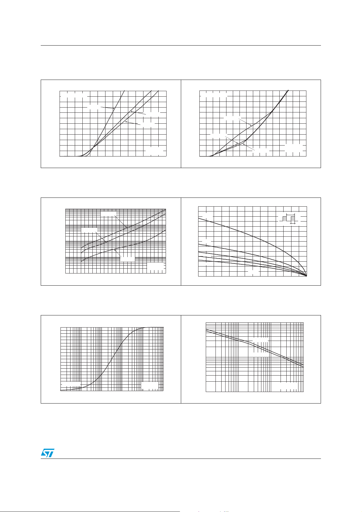
(A)
Figure 1. Forward voltage drop versus
forward current (typical values, low
level)
I
FM
12
Puse test : tp=380µs
10
8
6
4
2
0
0.0 0.5 1.0 1.5 2.0 2.5 3.0 3.5
Ta=25 °C
Ta=150 °C
Ta=175 °C
VFM(V)
Figure 3. Reverse leakage current versus
reverse voltage applied
(typical values)
IR(µA)
1.E+02
1.E+01
1.E+00
1.E-01
1.E-02
0 50 100 150 200 250 300 350 400 450 500 550 600 650
Tj=150 °C
Tj=175 °C
Tj=25 °C
VR(V)
Figure 2. Forward voltage drop versus
forward current (typical values,
high level)
IFM(A)
60
Puse test : tp=380µs
50
40
30
20
10
0
0.0 1.0 2.0 3.0 4.0 5.0 6.0 7.0 8.0
Ta=150 °C
Ta=25 °C
Ta=175 °C
VFM(V)
Figure 4. Peak forward current versus case
temperature
IM(A)
70
δ 0.1=
60
50
40
δ3= 0.
30
δ5= 0.
δ7= 0.
20
δ1=
10
0
0 25 50 75 100 125 150 175
TC(°C)
T
tp
= tp/T
δ
Figure 5. Relative variation of thermal
1.0
0.9
0.8
0.7
0.6
0.5
0.4
0.3
0.2
0.1
0.0
1.E-05 1.E-04 1.E-03 1.E-02 1.E-01 1.E+00
impedance junction to case
versus pulse duration
Z
th(j c)/Rth(j c)
Single pulse
tp(s)
Figure 6. Non-repetitive peak surge forward
current versus pulse duration
(sinusoidal waveform)
1.E+03
Ta=25 °C
1.E+02
1.E+01
1.E-05 1.E-04 1.E-03 1.E-02
Ta=125 °C
tp(s)
Doc ID 023247 Rev 1 3/9
 Loading...