

ST STPSC1206 User Manual
600 V power Schottky silicon carbide diode
Features
■ No reverse recovery
■ Switching behavior independent of
temperature
■ Dedicated to PFC boost diode
STPSC1206
Description
These diodes are manufactured using silicon
carbide substrate. This wide bandgap material
supports the manufacture of a Schottky diode
structure with a high voltage rating. Such diodes
exhibit no or negligible recovery characteristics.
The recovery characteristics are independent of
the temperature.
Using these diodes will significantly reduce the
switching power losses of the associated MOSFET, and thus increase the efficiency of the
overall application. These diodes will then
outperform the power factor correction circuit
operating in hard switching conditions.
K
TO-220AC
STPSC1206D
Table 1. Device summary
I
F(AV)
V
RRM
T
j (max)
Q
C (typ)
A
12 A
600 V
175 °C
12 nC
September 2009 Doc ID 16288 Rev 1 1/7
www.st.com
7
Characteristics STPSC1206
1 Characteristics
Table 2. Absolute ratings (limiting values at 25 °C unless otherwise specified)
Symbol Parameter Value Unit
V
RRM
I
F(RMS)
I
F(AV)
I
FSM
I
FRM
T
T
Table 3. Thermal resistance
Repetitive peak reverse voltage 600 V
Forward rms current 30 A
Average forward current Tc = 110 °C, δ = 0.5 12
t
= 10 ms sinusoidal, Tc = 25 °C
p
Surge non repetitive forward current
= 10 ms sinusoidal, Tc = 125 °C
t
p
= 10 µs square, Tc = 25 °C
t
p
Repetitive peak forward current Tc = 105 °C, Tj = 150 °C, δ = 0.1 50 A
Storage temperature range -55 to +175 °C
stg
Operating junction temperature -40 to +175 °C
j
50
40
200
Symbol Parameter Maximum value Unit
R
th(j-c)
Table 4. Static electrical characteristics
Junction to case 1.75 °C/W
Symbol Parameter Tests conditions Min. Typ. Max. Unit
(1)
I
R
V
F
1. tp = 10 ms, δ < 2%
= 500 µs, δ < 2%
2. t
p
Reverse leakage current
(2)
Forward voltage drop
Tj = 25 °C
VR = V
= 12 A
I
F
RRM
= 150 °C - 200 1500
T
j
T
= 25 °C
j
= 150 °C - 1.6 2.1
T
j
- 30 150
-1.41.7
A
A
µA
V
To evaluate the conduction losses use the following equation:
P = 1.2 x I
Table 5. Other parameters
Symbol Parameter Test conditions Typ. Unit
Q
c
C Total capacitance
2/7 Doc ID 16288 Rev 1
Total capacitive charge
+ 0.075 x I
F(AV)
F2(RMS)
V
= 400 V, IF = 12 A
r
dI
/dt = -200 A/µs, Tj = 150 °C
F
= 0 V, Tc = 25 °C, F = 1 Mhz 750
V
r
= 400 V, Tc = 25 °C, F = 1 Mhz 65
V
r
12 nC
pF
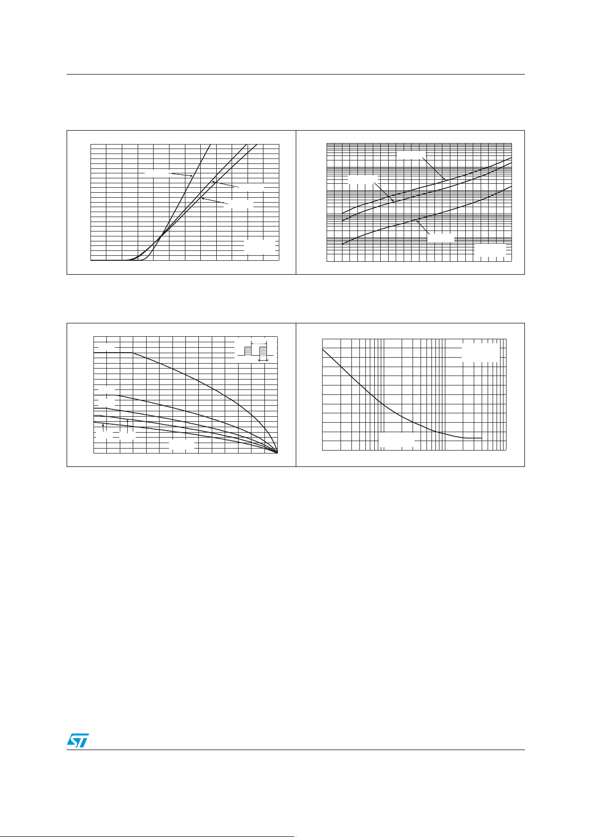
STPSC1206 Characteristics
Figure 1. Forward voltage drop versus
forward current (typical values)
IFM(A)
24
22
20
18
16
14
12
10
8
6
4
2
0
0.0 0.5 1.0 1.5 2.0 2.5 3.0
Tj=25 °CTj=25 °C
Tj=150 °CTj=150 °C
Tj=175 °CTj=175 °C
VFM(V)
Figure 3. Peak forward current versus case
temperature
IM(A)
110
δ=0.1
100
90
80
70
60
δ=0.3
50
δ=0.5
40
30
20
d=1δ=1
10
0
d=0.7δ=0.7
TC(°C)
0 25 50 75 100 125 150 175
δ
=tp/T
T
tp
Figure 2. Reverse leakage current versus
reverse voltage applied
(maximum values)
IR(µA)
1.E+04
Tj=175 °CTj=175 °C
1.E+03
Tj=150 °CTj=150 °C
1.E+02
1.E+01
1.E+00
1.E-01
0 50 100 150 200 250 300 350 400 450 500 550 600
Tj=25 °CTj=25 °C
VR(V)
Figure 4. Junction capacitance versus
reverse voltage applied
(typical values)
C(pF)
600
500
400
300
200
100
0
1 10 100 1000
VR(V)
V
OSC
F=1 MHz
=30 mV
Tj=25 °C
RMS
Doc ID 16288 Rev 1 3/7
 Loading...