


STPS61L60C
Power Schottky rectifier
Features
■ High current capability
■ Avalanche rated
■ Low forward voltage drop current
■ High frequency operation
Description
This dual center tap schottky rectifier is suited for
high frequency switch mode power supplies.
Packaged in TO-247 and TO-220AB, this device
provides desktop SMPS designers with a low
forward voltage drop device, and reduced leakage
current, with the objective of making the
application compliant with environmental care
standards, or suitable for 80+ requirements.
Table 1. Device summary
I
F(AV)
V
RRM
(max) 150 °C
T
j
(typ) 0.560 V
V
F
2 x 30 A
60 V
A1
K
A2
K
A2
K
A1
TO-247
STPS61L60CW
TO-220AB
STPS61L60CT
Figure 1. Electrical characteristics
2 x I
I
"Forward"
F(Io)
X
X
V
F
O
I
F
I
O
I
R
V
V
To
V
I
V
RRM
V
V
AR
R
"Reverse"
V
F(2xIo)
A1
(a)
A2
K
V
I
AR
a. V
ARM
and I
must respect the reverse safe
ARM
operating area defined in Figure 12 V
pulse measurements (t
are static characteristics
< 1 µs). VR, IR, V
p
and IAR are
AR
RRM
June 2010 Doc ID 15641 Rev 2 1/9
and VF,
www.st.com
9
Characteristics STPS61L60C
1 Characteristics
Table 2. Absolute ratings (limiting values per diode at 25 °C unless otherwise specified)
Symbol Parameter Value Unit
V
I
F(RMS)
I
F(AV)
I
P
V
ARM
V
ASM
T
1. Refer to Figure 12
2. condition to avoid thermal runaway for a diode on its own heatsink
Table 3. Thermal resistances
Repetitive peak reverse voltage 60 V
RRM
Forward rms voltage 50 A
= 125 °C
T
Average forward current δ = 0.5
Surge non repetitive forward current tp = 10 ms sinusoidal
FSM
Repetitive peak avalanche power tp = 1 µs Tj = 25 °C 11500 W
ARM
Maximum repetitive peak avalanche
(1)
voltage
Maximum single pulse peak
(1)
avalanche voltage
Storage temperature range -65 to + 175 °C
stg
T
Maximum operating junction temperature
j
<
Rth(j-a)
1
dPtot
dTj
c
= 120 °C
T
c
t
< 1 µs Tj < 150 °C, IAR < 43 A 80 V
p
< 1 µs Tj < 150 °C, IAR < 43 A 80 V
t
p
(2)
Per diode
Per device
T0-247
T0-220AB
30
60
530
400
150 °C
Symbol Parameter Value Unit
A
A
R
R
th(j-c)
th(c)
Junction to case
Coupling
When the diodes 1 and 2 are used simultaneously :
ΔTj(diode 1) = P(diode1) x R
(Per diode) + P(diode 2) x R
th(j-c)
TO-247
TO-220AB
.
th(c)
Per diode
To t al
Per diode
To t al
0.95
0.6
1.1
0.7
TO-247 0.25
TO-220AB 0.3
°C/W
2/9 Doc ID 15641 Rev 2

STPS61L60C Characteristics
Table 4. Static electrical characteristics (per diode)
Symbol Parameter Test conditions Min. Typ. Max. Unit
= 25 °C
T
(1)
I
Reverse leakage current
R
j
Tj = 125 °C - 150 350
V
= V
R
RRM
--0.8
Tj = 25 °C IF = 5 A - 0.360 -
T
= 125 °C IF = 5 A - 0.255 -
j
(2)
V
Forward voltage drop
F
Tj = 25 °C IF = 15 A - 0.460 0.540
Tj = 125 °C IF = 15 A - 0.415 0.480
T
= 25 °C IF = 30 A - 0.580 0.660
j
Tj = 125 °C IF = 30 A - 0.560 0.620
1. Pulse test: tp = 5 ms, δ < 2%
2. Pulse test: t
To evaluate the conduction losses use the following equation: P = 0.44 x I
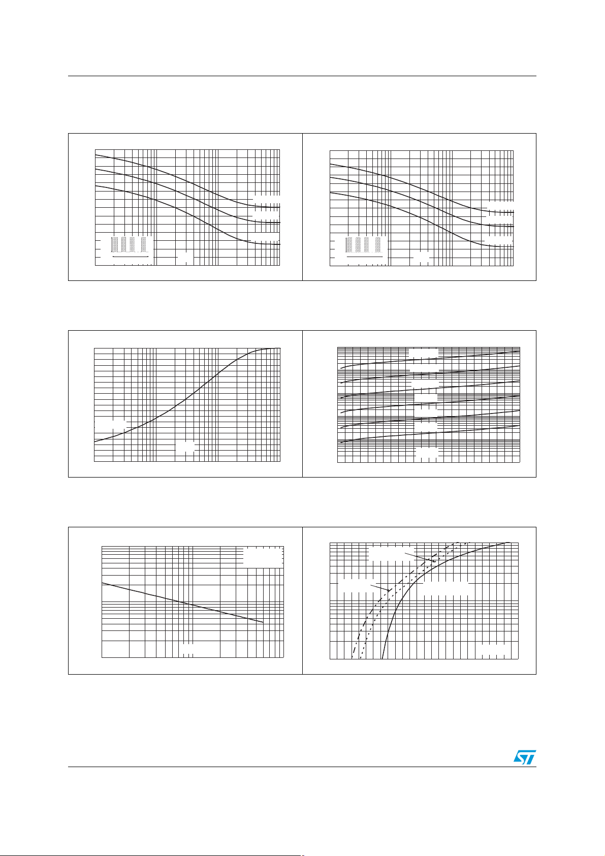
Figure 2. Average forward power dissipation
P (W)
F(av)
30
25
20
15
10
5
0
0 5 10 15 20 25 30 35 40
Figure 4. Normalized avalanche power
= 380 µs, δ < 2%
p
vs. average forward current
(per diode)
δ=0.2
δ=0.1
δ=0.05
I (A)
F(av)
δ=0.5
δ
=tp/T
derating vs. pulse duration
+ 0.006 x I
F(AV)
F2(RMS)
Figure 3. Average forward current vs.
ambient temperature
(δ = 0.5, per diode)
I (A)
F(av)
δ=1
T
tp
35
30
25
20
15
10
5
0
T
=tp/T
δ
0 25 50 75 100 125 150
R
th(j-a)=Rth(j-c)
TO-220AB
R
=15 °C/W
th(j-a)
tp
T
amb
(°C)
TO-247
Figure 5. Normalized avalanche power
derating vs. junction temperature
mA
V
P(t)
ARM p
P (1µs)
ARM
1
0.1
0.01
t (µs)
0.001
0.10.01 1
p
10 100 1000
P(T)
ARM
j
P (25 °C)
ARM
1.2
1
0.8
0.6
0.4
0.2
0
25 50 75 100 125 150
T (°C)
j
Doc ID 15641 Rev 2 3/9
Characteristics STPS61L60C
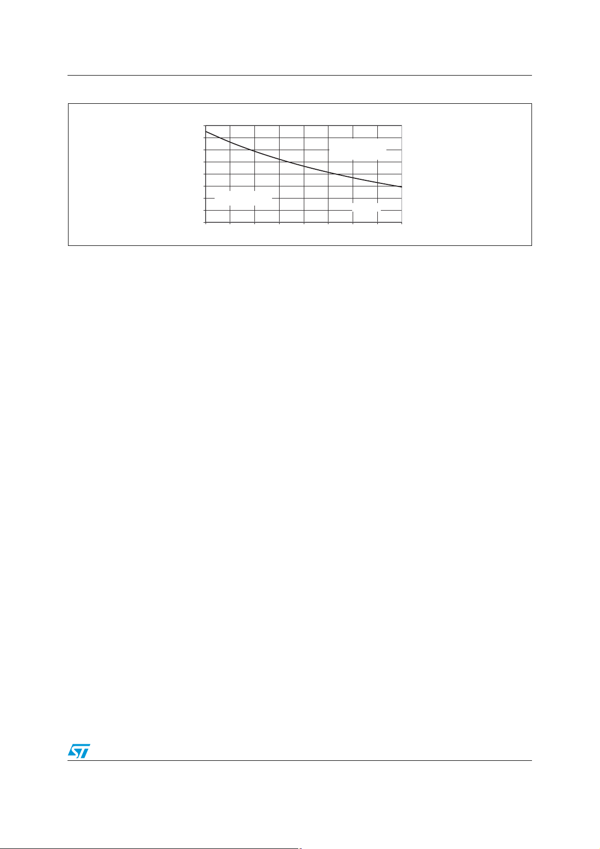
Figure 6. Non repetitive surge peak forward
current vs. overload duration
(max. values, per diode, TO-247)
I (A)
M
350
300
250
200
150
100
I
M
50
0
1.E-03 1.E-02 1.E-01 1.E+00
δ=0.5
t
t(s)
Tc=25 °C
Tc=75 °C
Tc=125 °C
Figure 8. Relative variation of thermal
impedance junction to case
vs. pulse duration
Z/R
th(j-c) th(j-c)
1.0
0.9
0.8
0.7
0.6
0.5
0.4
Single pulse
0.3
0.2
0.1
0.0
1.E-03 1.E-02 1.E-01 1.E+00
t (s)
p
Figure 10. Junction capacitance vs. reverse
voltage applied
(typical values, per diode)
C(pF)
10000
V
osc
F=1 MHz
=30 mV
Tj=25 °C
RMS
Figure 7. Non repetitive surge peak forward
current vs. overload duration
(max. values, per diode, TO-220AB)
I (A)
M
350
300
250
200
150
100
I
M
50
0
1.E-03 1.E-02 1.E-01 1.E+00
δ=0.5
t
t(s)
Tc=25 °C
Tc=75 °C
Tc=125 °C
Figure 9. Reverse leakage current vs. reverse
voltage applied
(typical values, per diode)
I (mA)
R
1.E+03
1.E+02
1.E+01
1.E+00
1.E-01
1.E-02
0 5 10 15 20 25 30 35 40 45 50 55 60
Tj=150 °C
Tj=125 °C
Tj=100 °C
Tj=75 °C
Tj=50 °C
Tj=25 °C
V (V)
R
Figure 11. Forward voltage drop vs. forward
current (per diode)
I (A)
FM
100
TJ=125 °C
TJ=125 °C
Maximum values
Maximum values
1000
V (V)
100
1 10 100
R
4/9 Doc ID 15641 Rev 2
TJ=125 °C
TJ=125 °C
Typical values
Typical values
10
1
0.0 0.1 0.2 0.3 0.4 0.5 0.6 0.7 0.8 0.9 1.0 1.1 1.2 1.3
TJ=25 °C
Maximum values
V (V)
FM
STPS61L60C Characteristics
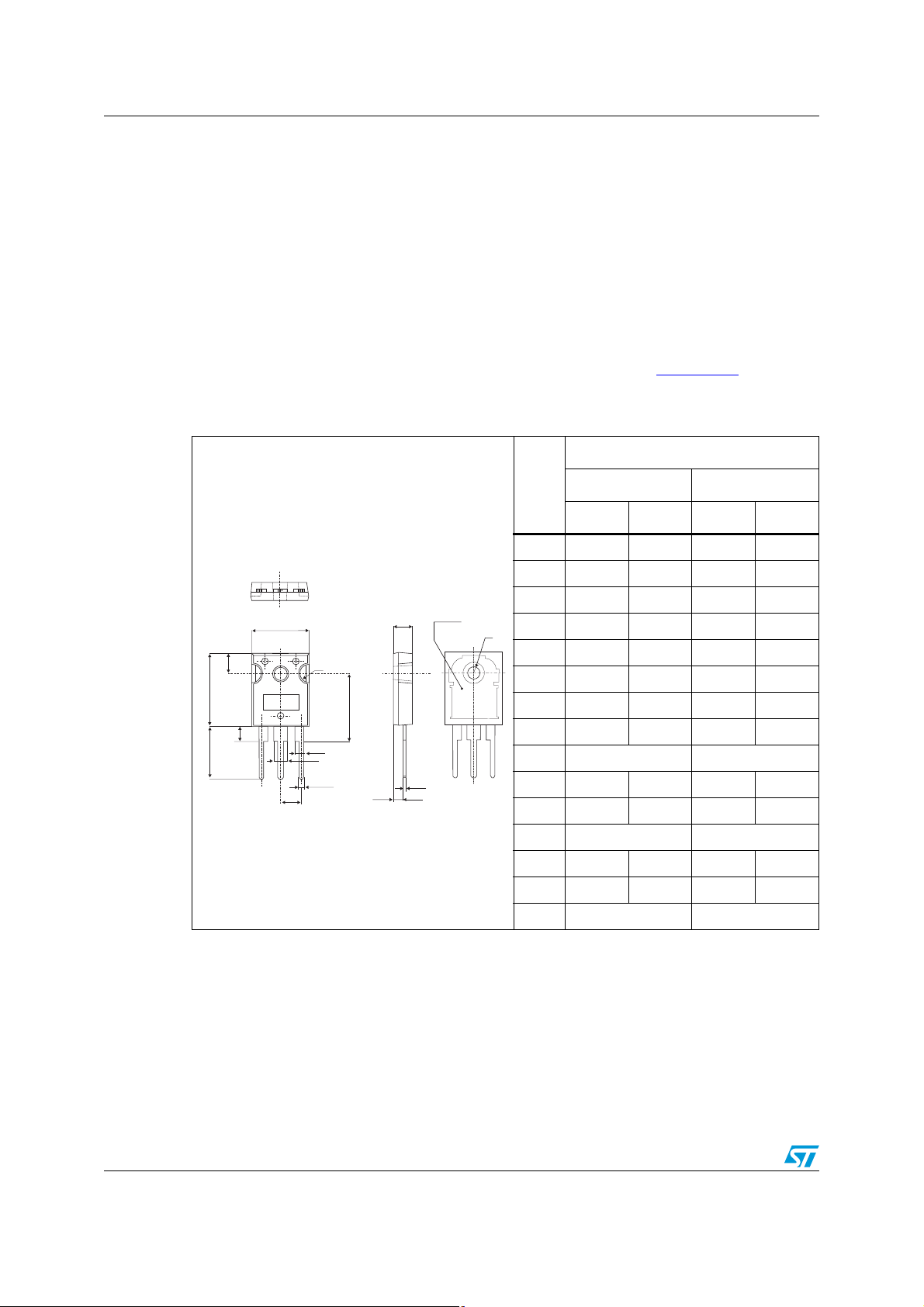
Figure 12. Reverse safe operating area (tp < 1 µs and Tj < 150 °C)
Iarm (A)
60
55
50
45
40
35
Operating area
30
25
20
60 65 70 75 80 85 90 95 100
Forbidden area
Varm(V)
Doc ID 15641 Rev 2 5/9
Package information STPS61L60C
2 Package information
● Epoxy meets UL94, V0
● Cooling method: conduction
● Torque value:
– TO-247 - 0.55 N·m recommended, 1.0 N·m maximum
– TO-220AB - 0.4 to 0.6 N·m
In order to meet environmental requirements, ST offers these devices in different grades of
ECOPACK
specifications, grade definitions and product status are available at: www.st.com
ECOPACK
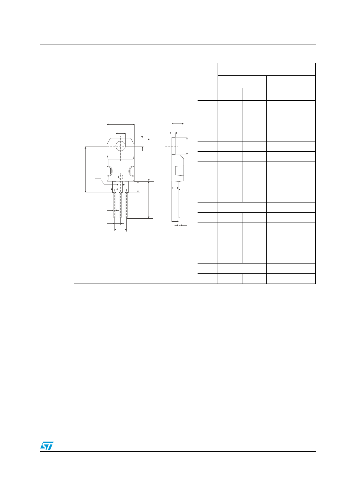
Table 5. TO-247 dimensions
®
packages, depending on their level of environmental compliance. ECOPACK®
®
is an ST trademark.
.
Dimensions
Ref.
Millimeters Inches
Min. Max. Min. Max.
A 4.85 5.15 0.191 0.203
A1 2.20 2.60 0.086 0.102
b 1.00 1.40 0.039 0.055
Heat-sink plane
E
S
D
L1
L
11223
∅R
L2
b1
b2
b
e
A
b1 2.00 2.40 0.078 0.094
∅P
b2 3.00 3.40 0.118 0.133
c 0.40 0.80 0.015 0.031
(1)
D
19.85 20.15 0.781 0.793
E 15.45 15.75 0.608 0.620
e 5.45 typ. 0.215 typ.
3
c
A1
BACK VIEW
L 14.20 14.80 0.559 0.582
L1 3.70 4.30 0.145 0.169
L2 18.50 typ. 0.728 typ.
(2)
∅P
3.55 3.65 0.139 0.143
1. Dimension D plus gate protrusion does not exceed 20.5 mm
2. Resin thickness around the mounting hole is not less than 0.9 mm
6/9 Doc ID 15641 Rev 2
∅R 4.50 5.50 0.177 0.217
S 5.50 typ. 0.216 typ.
STPS61L60C Package information
Table 6. TO-220AB dimensions
Dimensions
L2
F2
F1
F
G1
H2
Dia
Ref.
Millimeters Inches
Min. Max. Min. Max.
A 4.40 4.60 0.173 0.181
A
C
C 1.23 1.32 0.048 0.051
D 2.40 2.72 0.094 0.107
E 0.49 0.70 0.019 0.027
L5
L6
L7
F 0.61 0.88 0.024 0.034
F1 1.14 1.70 0.044 0.066
F2 1.14 1.70 0.044 0.066
G 4.95 5.15 0.194 0.202
L9
L4
D
G1 2.40 2.70 0.094 0.106
H2 10 10.40 0.393 0.409
L2 16.4 typ. 0.645 typ.
M
E
L4 13 14 0.511 0.551
L5 2.65 2.95 0.104 0.116
G
L6 15.25 15.75 0.600 0.620
L7 6.20 6.60 0.244 0.259
L9 3.50 3.93 0.137 0.154
M 2.6 typ. 0.102 typ.
Diam. 3.75 3.85 0.147 0.151
Doc ID 15641 Rev 2 7/9

Ordering information STPS61L60C
3 Ordering information
Table 7. Ordering information
Order code Marking Package Weight Base qty Delivery mode
STPS61L60CW STPS61L60CW TO-247 4.4 g 30 Tube
STPS61L60CT STPS61L60CT TO-220AB 2.23 g 30 Tube
4 Revision history
Table 8. Document revision history
Date Revision Changes
18-May-2009 1 Initial release.
29-Jun-2010 2
Added Figure 1 and Figure 12. Added parameters V
V
to Ta b l e 2 . Updated Tabl e 5 .
ASM
ARM
and
8/9 Doc ID 15641 Rev 2

STPS61L60C
Please Read Carefully:
Information in this document is provided solely in connection with ST products. STMicroelectronics NV and its subsidiaries (“ST”) reserve the
right to make changes, corrections, modifications or improvements, to this document, and the products and services described herein at any
time, without notice.
All ST products are sold pursuant to ST’s terms and conditions of sale.
Purchasers are solely responsible for the choice, selection and use of the ST products and services described herein, and ST assumes no
liability whatsoever relating to the choice, selection or use of the ST products and services described herein.
No license, express or implied, by estoppel or otherwise, to any intellectual property rights is granted under this document. If any part of this
document refers to any third party products or services it shall not be deemed a license grant by ST for the use of such third party products
or services, or any intellectual property contained therein or considered as a warranty covering the use in any manner whatsoever of such
third party products or services or any intellectual property contained therein.
UNLESS OTHERWISE SET FORTH IN ST’S TERMS AND CONDITIONS OF SALE ST DISCLAIMS ANY EXPRESS OR IMPLIED
WARRANTY WITH RESPECT TO THE USE AND/OR SALE OF ST PRODUCTS INCLUDING WITHOUT LIMITATION IMPLIED
WARRANTIES OF MERCHANTABILITY, FITNESS FOR A PARTICULAR PURPOSE (AND THEIR EQUIVALENTS UNDER THE LAWS
OF ANY JURISDICTION), OR INFRINGEMENT OF ANY PATENT, COPYRIGHT OR OTHER INTELLECTUAL PROPERTY RIGHT.
UNLESS EXPRESSLY APPROVED IN WRITING BY AN AUTHORIZED ST REPRESENTATIVE, ST PRODUCTS ARE NOT
RECOMMENDED, AUTHORIZED OR WARRANTED FOR USE IN MILITARY, AIR CRAFT, SPACE, LIFE SAVING, OR LIFE SUSTAINING
APPLICATIONS, NOR IN PRODUCTS OR SYSTEMS WHERE FAILURE OR MALFUNCTION MAY RESULT IN PERSONAL INJURY,
DEATH, OR SEVERE PROPERTY OR ENVIRONMENTAL DAMAGE. ST PRODUCTS WHICH ARE NOT SPECIFIED AS "AUTOMOTIVE
GRADE" MAY ONLY BE USED IN AUTOMOTIVE APPLICATIONS AT USER’S OWN RISK.
Resale of ST products with provisions different from the statements and/or technical features set forth in this document shall immediately void
any warranty granted by ST for the ST product or service described herein and shall not create or extend in any manner whatsoever, any
liability of ST.
ST and the ST logo are trademarks or registered trademarks of ST in various countries.
Information in this document supersedes and replaces all information previously supplied.
The ST logo is a registered trademark of STMicroelectronics. All other names are the property of their respective owners.
© 2010 STMicroelectronics - All rights reserved
Australia - Belgium - Brazil - Canada - China - Czech Republic - Finland - France - Germany - Hong Kong - India - Israel - Italy - Japan -
STMicroelectronics group of companies
Malaysia - Malta - Morocco - Philippines - Singapore - Spain - Sweden - Switzerland - United Kingdom - United States of America
www.st.com
Doc ID 15641 Rev 2 9/9
 Loading...