

ST STPS61L45C User Manual
STPS61L45C
Power Schottky rectifier
Features
■ High current capability
■ Avalanche rated
■ Low forward voltage drop current
■ High frequency operation
Description
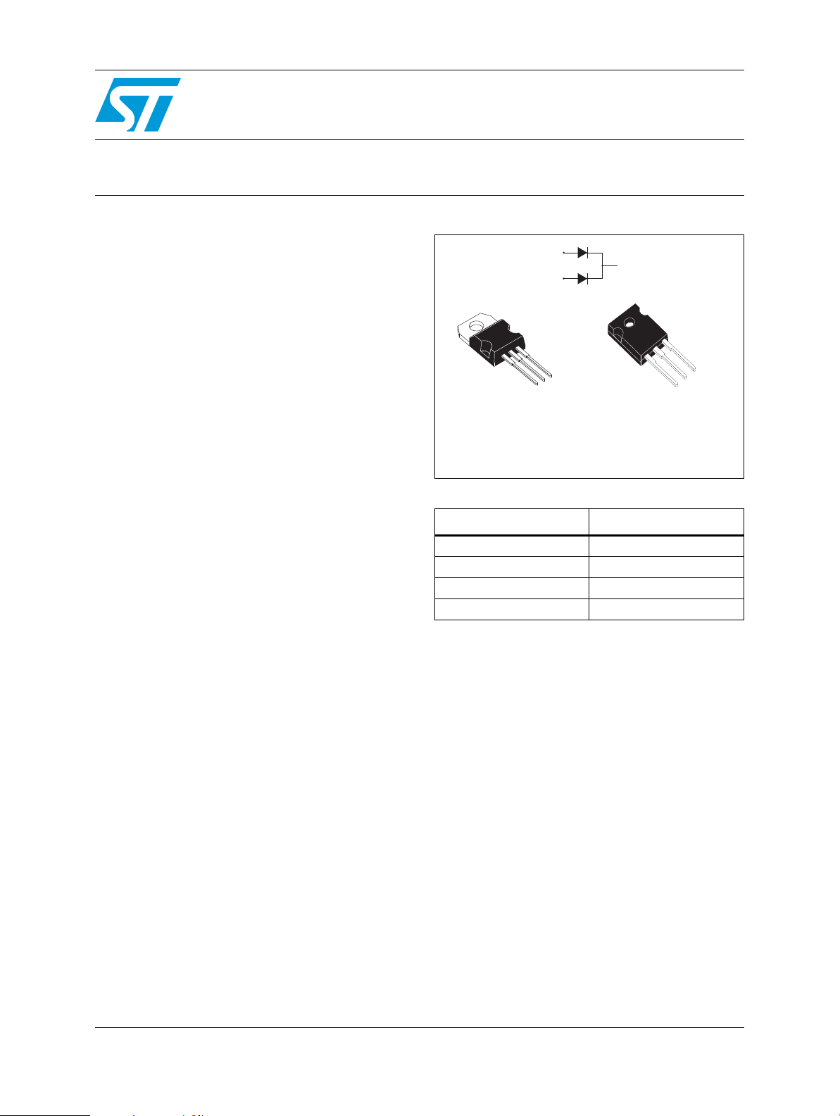
Dual center tap Schottky rectifier suited for high
frequency switch mode power supplies.
Packaged in TO-247 and TO-220AB, this device
provides desktop SMPS designers with a low
forward voltage drop device, and reduced leakage
current, with the objective of making the
application compliant with environmental care
standards, or suitable for 80+ requirements.
A1
A2
K
A2
K
A1
TO-220AB
STPS61L45CT
Table 1. Device summary
STPS61L45CW
Symbol Value
I
F(AV)
V
RRM
(max) 150 °C
T
j
(typ) 0.45 V
V
F
K
A2
K
A1
TO-247
2 x 30 A
45 V
July 2011 Doc ID 14192 Rev 2 1/8
www.st.com
8
Characteristics STPS61L45C
1 Characteristics
Table 2. Absolute ratings (limiting values per diode at 25 °C unless otherwise
specified)
Symbol Parameter Value Unit
V
RRM
I
F(RMS)
I
F(AV)
I
FSM
P
ARM
T
1. condition to avoid runaway for a diode on its own heatsink
Table 3. Thermal resistances
Repetitive peak reverse voltage 45 V
Forward rms current 60 A
Average forward current δ = 0.5
= 120 °C
c
Tc = 115 °C
Per diode
Per device
T
Surge non repetitive forward current tp = 10 ms sinusoidal 500 A
Repetitive peak avalanche power tp = 1 µs Tj = 25 °C 10000 W
Storage temperature range -65 to + 175 °C
stg
Maximum operating junction temperature
T
j
<
Rth(j-a)
1
dPtot
dTj
(1)
30
60
150 °C
Symbol Parameter Value Unit
R
R
th(j-c)
th(c)
Junction to case
Per diode
To t al
Coupling 0.2 °C/W
1.3
0.75
°C/W
When the diodes 1 and 2 are used simultaneously :
ΔTj(diode 1) = P(diode1) x R
Table 4. Static electrical characteristics (per diode)
Symbol Parameter Test conditions Min. Typ. Max. Unit
(Per diode) + P(diode 2) x R
th(j-c)
th(c)
.
A
T
= 25 °C
(1)
I
Reverse leakage current
R
j
= 125 °C 190 400
T
j
T
= 25 °C
j
Tj = 125 °C 0.23
T
= 25 °C
(2)
V
1. Pulse test: tp = 5 ms, δ < 2%
2. Pulse test: tp = 380 µs, δ < 2%
Forward voltage drop
F
j
= 125 °C 0.34 0.40
T
j
= 25 °C
T
j
T
= 125 °C 0.45 0.51
j
To evaluate the conduction losses use the following equation:
P = 0.3 x I
2/8 Doc ID 14192 Rev 2
+ 0.007 x I
F(AV)
F2(RMS)
= V
V
R
RRM
= 5 A
I
F
IF = 15 A
= 30 A
I
F
1.5
mA
0.35
0.43 0.50
V
0.50 0.56
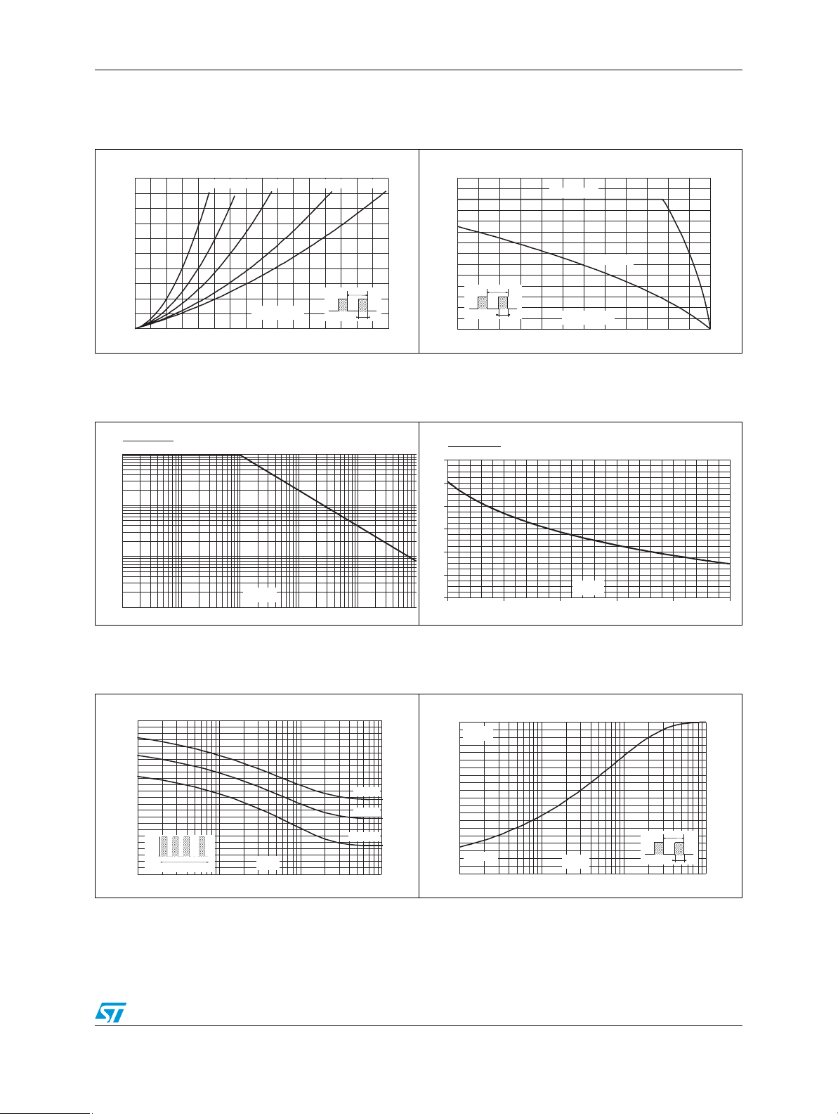
STPS61L45C Characteristics
0
Figure 1. Conduction losses versus average
forward current (per diode)
P (W)
F(av)
25
20
15
10
5
0
0 5 10 15 20 25 30 35 40
δ=0.05 δ=0.1 δ=0.2 δ=0.5 δ=1
I (A)
F(av)
δ
=tp/T
T
tp
Figure 3. Normalized avalanche power
derating versus pulse duration
P(tp)
ARM
P (1 µs)
ARM
1
0.1
0.01
t (µs)
.001
0.10.01 1
p
10 100 100
Figure 5. Non repetitive surge peak forward
current versus overload duration
(per diode)
Figure 2. Average forward current versus
ambient temperature (δ = 0.5),
(per diode)
I (A)
F(av)
35
R
30
25
20
15
10
5
0
T
tp
=tp/T
δ
0 25 50 75 100 125 150
th(j-a)=Rth(j-c)
T
amb
R
th(j-a)
(°C)
=10°C/W
Figure 4. Normalized avalanche power
derating versus junction
temperature
P(Tj)
ARM
P (25 °C)
ARM
1.2
1
0.8
0.6
0.4
0.2
0
25 50 75 100 125 150
T (°C)
j
Figure 6. Relative variation of thermal
impedance junction to case versus
pulse duration
I (A)
M
300
250
200
150
100
I
M
50
0
1.E-03 1.E-02 1.E-01 1.E+00
t
=0.5
δ
t(s)
TC=25°C
TC=75°C
TC=125°C
Doc ID 14192 Rev 2 3/8
Z/R
th(j-c) th(j-c)
1.0
TO-247
0.9
0.8
0.7
0.6
0.5
0.4
0.3
0.2
Single pulse
0.1
0.0
1.E-03 1.E-02 1.E-01 1.E+00
t (s)
p
δ
=tp/T
T
tp
 Loading...