

ST STPS61170C User Manual
Features
■ High junction temperature capability
■ Low leakage current
■ Good trade off between leakage current and
forward voltage drop
■ Low thermal resistance
■ High frequency operation
■ Avalanche specification
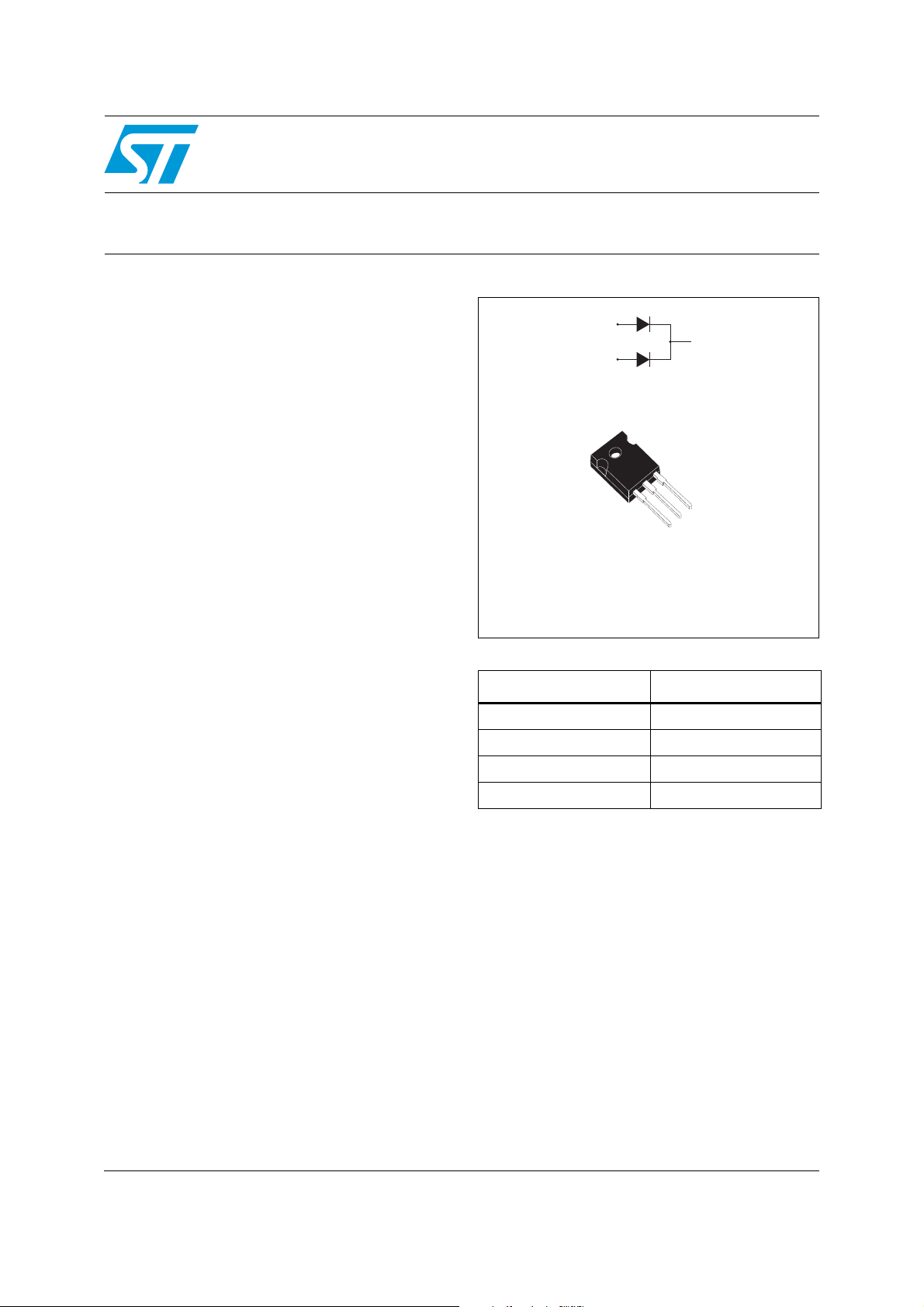
Description
Dual center tab Schottky rectifier suited for high
frequency switched mode power supply.
Packaged in TO-247, this device is intended for
use to enhance the reliability of the application.
STPS61170C
High voltage power Schottky rectifier
A1
K
A2
A2
K
A1
TO-247
Table 1. Device summary
Symbol Value
I
2 x 30 A
F(AV)
V
RRM
T
V
F (max)
j
170 V
175 °C
0.67 V
December 2010 Doc ID 11643 Rev 2 1/7
www.st.com
7

Characteristics STPS61170C
1 Characteristics
Table 2. Absolute ratings (limiting values, per diode)
Symbol Parameter Value Unit
V
I
F(RMS)
I
F(AV)
I
P
V
ARM
V
ASM
T
Repetitive peak reverse voltage 170 V
RRM
Forward rms current 80 A
Average forward current T
Surge non repetitive forward current t
FSM
Repetitive peak avalanche power tp = 1 µs Tj = 25 °C 31800 W
ARM
(1)
Maximum repetitive peak avalanche voltage
(1)
Maximum single pulse peak avalanche voltage
Storage temperature range -65 to + 175 °C
stg
T
Maximum operating junction temperature
j
= 150 °C δ = 0.5
C
(2)
p
t
p
I
AR
Per diode
Per device
= 10 ms sinusoidal 500 A
= 1 µs, Tj < 150 °C,
< 47 A
30
60
200 V
175 °C
dV/dt Critical rate of rise reverse voltage 10000 V/µs
1. Refer to Figure 11
dPtot
2. condition to avoid thermal runaway for a diode on its own heatsink
dTj
Table 3. Thermal resistance parameters
<
Rth(j-a)
1
Symbol Parameter Value Unit
A
R
Junction to case
th (j-c)
R
Coupling 0.3
th (c)
Per diode
To t al
0.9
0.6
°C/W
When the diodes 1 and 2 are used simultaneously :
ΔT
(diode 1) = P(diode1) x R
j
Table 4. Static electrical characteristics (per diode)
(Per diode) + P(diode 2) x R
th(j-c)
th(c)
Symbol Parameter Tests conditions Min. Typ. Max. Unit
= 25 °C
(1)
I
R
VF
1. Pulse test: tp = 5 ms, δ < 2%
2. Pulse test: t
Reverse leakage current
(2)
Forward voltage drop
= 380 µs, δ < 2%
p
T
j
= 125 °C 16 60 mA
T
j
= 25 °C
T
j
T
= 125 °C 0.63 0.67
j
= 25 °C
T
j
Tj = 125 °C 0.76 0.80
V
= V
R
= 30 A
I
F
= 60 A
I
F
RRM
60 µA
0.84
V
0.92
To evaluate the conduction losses use the following equation :
P = 0.54 x I
F(AV)
+ 0.0043 I
F2(RMS)
2/7 Doc ID 11643 Rev 2
STPS61170C Characteristics
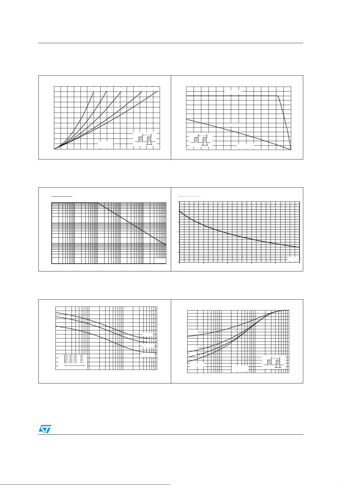
Figure 1. Average forward power dissipation
versus average forward current
(per diode)
P
(W)
F(AV)
30
25
20
15
10
5
0
0 5 10 15 20 25 30 35 40
d=0.05 d=0.1
I
F(AV)
d=0.2
(A)
d
=t /T
d=1
d=0.5
T
t
p
p
Figure 3. Normalized avalanche power
derating versus pulse duration
P(tp)
ARM
P(t)
ARM p
P (1µs)
ARM
P (1µs)
ARM
1
1
0.1
0.1
0.01
0.01
t (µs)
p
10 100 1000
10 100
t (µs)
p
1000
0.001
0.001
0.10.01 1
0.10.01 1
Figure 2. Average forward current versus
ambient temperature
(δ = 0.5, per diode)
I
(A)
F(AV)
35
30
25
20
15
10
5
0
T
t
=t /T
p
p
d
0 25 50 75 100 125 150 175
R
th(j-a)=Rth(j-c)
R
th(j-a)
=15°C/W
T
(°C)
amb
Figure 4. Normalized avalanche power
derating versus junction
temperature
P(T)
ARM j
P(t)
ARM p
P (25 °C)
ARM
1.2
P (25°C)
ARM
1.2
1
1
0.8
0.8
0.6
0.6
0.4
0.4
0.2
0.2
0
25
0
25 50 75 100 125
50 75 100 125 150
T (°C)
j
T (°C)
j
150
Figure 5. Non repetitive surge peak forward
current versus overload duration
(maximum values, per diode)
IM(A)
400
350
300
250
200
150
100
I
M
50
0
1.E-03 1.E-02 1.E-01 1.E+00
d=0.5
t
t(s)
TC=50°C
TC=75°C
TC=125°C
Doc ID 11643 Rev 2 3/7
Figure 6. Relative variation of thermal
impedance junction to case versus
pulse duration (per diode)
Z
th(j-c)/Rth(j-c)
1.0
0.9
0.8
0.7
d=0.5
0.6
0.5
d=0.2
0.4
d=0.1
0.3
0.2
Single pulse
0.1
0.0
1.E-03 1.E-02 1.E-01 1.E+00
tP(s)
T
=t /T
p
d
t
p
 Loading...