

ST STPS60L30C-Y User Manual
STPS60L30C-Y
Automotive power Schottky rectifier
Features
■ Very small conduction losses
■ Negligible switching losses
■ Extremely fast switching
■ AEC-Q101 qualified
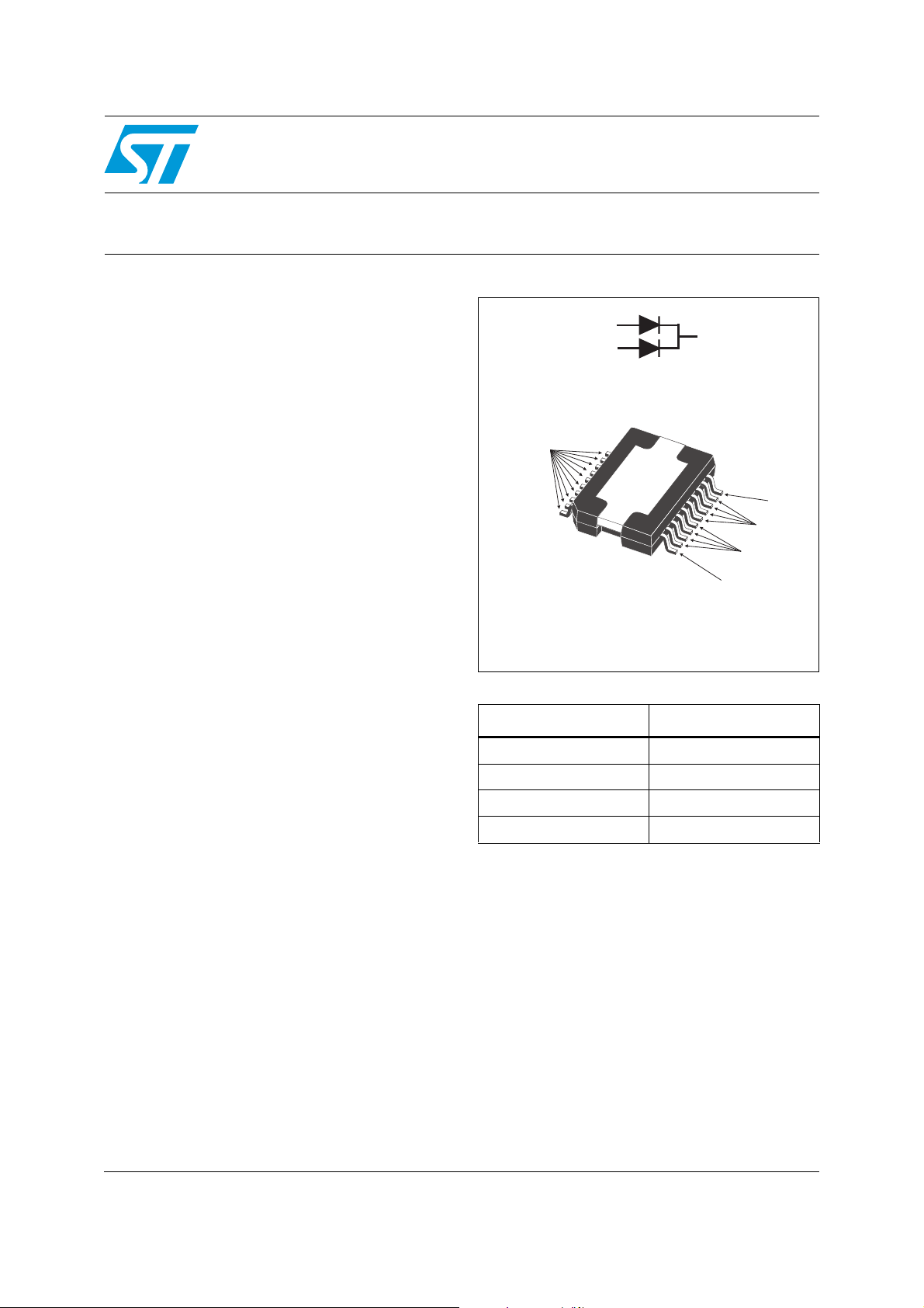
Description
60 A dual center tab Schottky rectifier suitable for
automotive applications.
Packaged in PowerSO-20 (slug up), this device is
especially intended for use in a low voltage
applications.
A1
A2
Pin 10
K
K
Pin 1
Pin 20
PowerSO-20 (slug up)
STPS60L30CKY-TR
Table 1. Device summary
Symbol Value
I
F(AV)
V
RRM
T
j(max)
V
F(max)
K
Pin 11
K
A1
A2
K
2 x 30 A
30 V
150 °C
0.415 V
December 2010 Doc ID 18296 Rev 1 1/7
www.st.com
7

Characteristics STPS60L30C-Y
1 Characteristics
Table 2. Absolute rating (limiting value, per diode)
Symbol Parameter Value Unit
V
RRM
IF
(RMS)
IF
(AV)
I
FSM
T
T
1. All anode pins (A1, A2) must be connected
Repetitive peak reverse voltage 30 V
(1)
Forward rms current 45 A
T
= 130 °C, δ = 0.5
(1)
Average forward current
(1)
Surge non repetitive forward current tp = 10 ms Sinusoidal 250 A
Storage temperature range -65 to +175 °C
stg
T
Operating junction temperature range -40 to +150 °C
j
Recommended reflow soldering temperature range 245 +0/-5 °C
R
c
Square pulse
Per diode
Per device
30
60
Table 3. Thermal parameters
Symbol Parameter Value Unit
R
R
th(j-c)
th(c)
Junction to case
Per diode
Per device
Coupling 0.27 °C/W
0.95
0.61
°C/W
When diodes 1 and 2 are used simultaneously:
ΔT
j(diode 1)
Table 4. Static electrical characteristics (per diode)
= P
(diode1)
x R
th(j-c)(Per diode)
+ P
(diode 2)
x R
th(c)
A
Symbol Parameter Test conditions Min. Typ. Max. Unit
= 25 °C
T
R
(1)
V
F
1. Pulse test : tp = 380 µs, δ < 2%
2. All anode pins (A1, A2) must be connected
current
(2)
Forward voltage drop
Reverse leakage
(1)
I
j
= 125 °C 400 mA
T
j
= 25 °C IF = 10 A 0.420
T
j
T
= 125 °C IF = 10 A 0.310
j
= 25 °C IF = 30 A 0.490
T
j
= 125 °C IF = 30 A 0.415
T
j
V
R
To evaluate the maximum conduction losses use the following equation:
P = 0.315 x I
2/7 Doc ID 18296 Rev 1
+ 0.00333 x I
F(AV)
F2(RMS)
= V
2mA
RRM
V
STPS60L30C-Y Characteristics
R=R
th(j-a) th(j-c)
R=10°C/W
th(j-a)
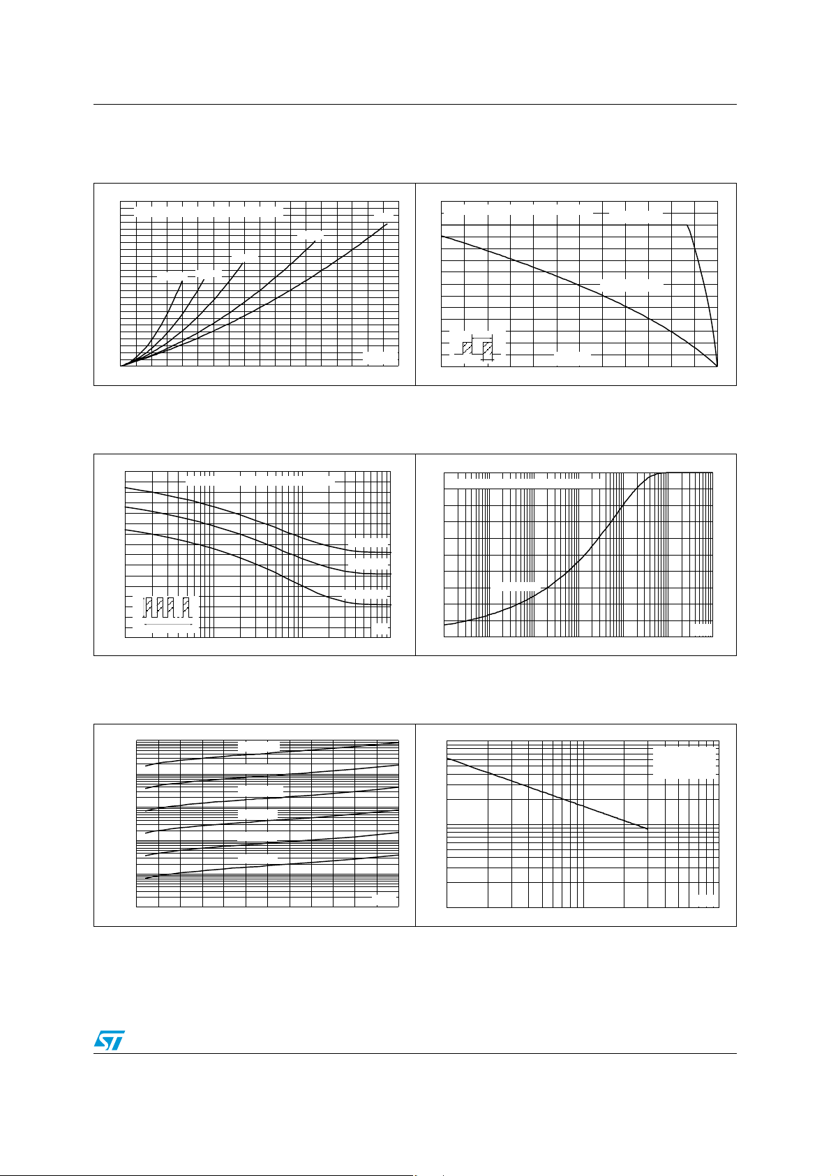
Figure 1. Average forward power dissipation
versus average forward current
P (W)
F(AV)
24
(per diode, all anode pins connected)
22
20
18
16
14
12
10
8
6
4
2
0
δ = 0.05
0 5 10 15 20 25 30 35 40 45
δ = 0.2
δ = 0.1
δ = 0.5
δ = 1
I (A)
F(AV)
Figure 3. Non repetetive surge peak forward
current versus overload duration
(maximum values)
I (A)
M
400
350
300
250
200
150
100
I
M
50
0
1.E-03 1.E-02 1.E-01 1.E+00
(per diode, all anode pins connected)
t
δ = 0.5
T = 25 °C
c
T = 75 °C
c
T = 125 °C
c
t(s)
Figure 5. Reverse leakage current versus
reverse voltage applied (per diode)
(typical values)
I (mA)
R
1.E+03
1.E+02
1.E+01
1.E+00
1.E-01
T = 150 °C
j
T = 125 °C
j
T = 100 °C
j
T = 75 °C
j
T = 50 °C
j
T = 25 °C
j
Figure 2. Average forward current versus
ambient temperature per diode
(δ = 0.5)
I (A)
F(AV)
35
(per diode, all anode pins connected)
30
25
20
15
10
5
0
T
δ = t / T
0 25 50 75 100 125 150
t
p
p
T (°C)
amb
R=R
th(j-a) th(j-c)
R=10°C/W
th(j-a)
Figure 4. Relative variation of thermal
impedance, junction to case,
versus pulse duration
Z/R
th(j-c) th(j-c)
1.0
(per diode, all anode pins connected)
0.9
0.8
0.7
0.6
0.5
0.4
0.3
0.2
0.1
0.0
1.E-05 1.E-04 1.E-03 1.E-02 1.E-01 1.E+00 1.E+01
Single pulse
t (s)
p
Figure 6. Junction capacitance versus
reverse voltage applied (per diode)
(typical values)
C(nF)
10.0
1.0
F = 1 MHz
V = 30 mV
osc RMS
T = 25 °C
j
1.E-02
0 5 10 15 20 25 30
V (V)
R
0.1
1 10 100
V (V)
R
Doc ID 18296 Rev 1 3/7
 Loading...