

ST STPS6045CP, STPS6045CPI, STPS6045CW User Manual
®
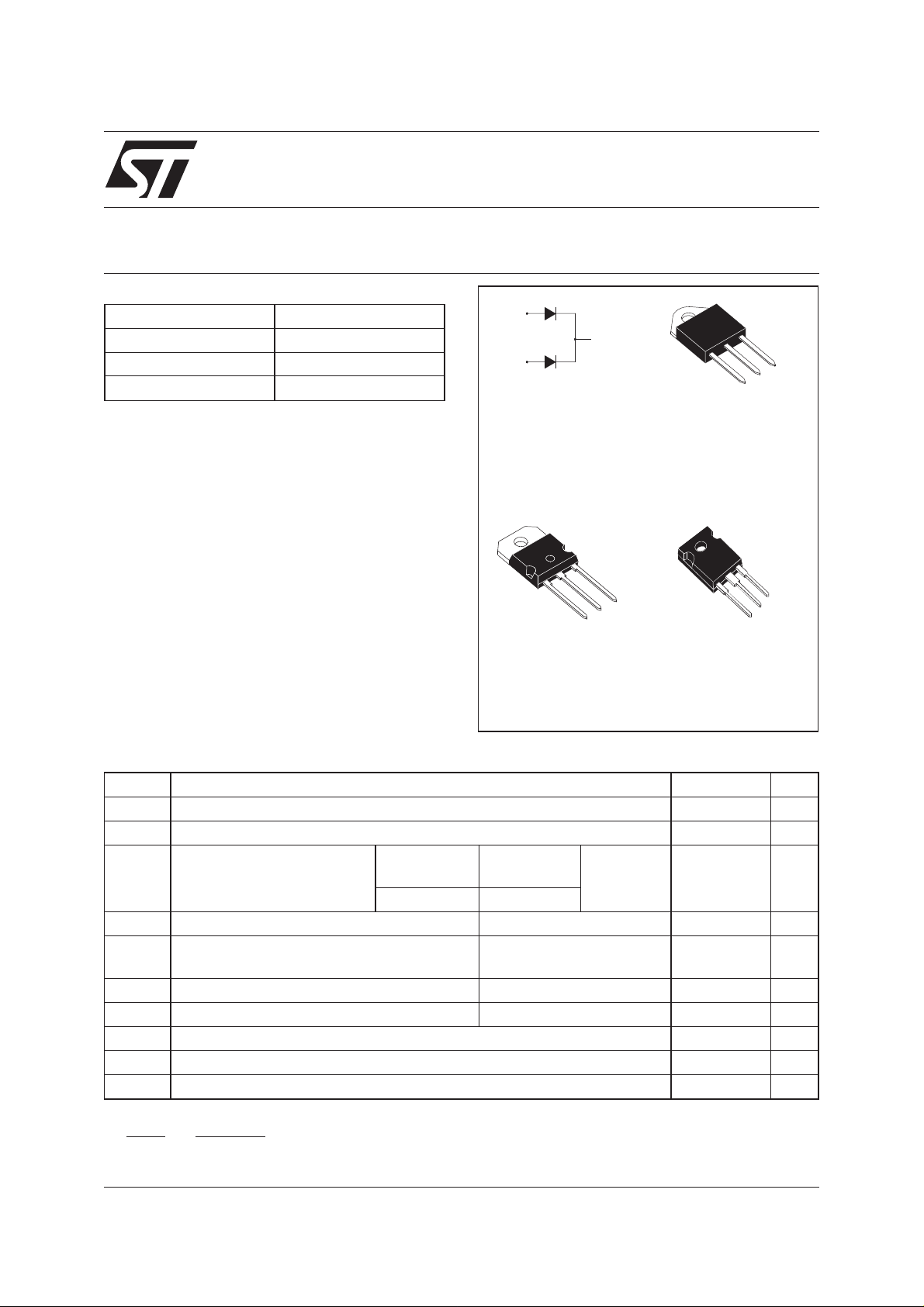
MAIN PRODUCT CHARACTERISTICS
I
F(AV)
V
RRM
2x30 A
45 V
Tj (max) 175 °C
V
(max) 0.63 V
F
STPS6045CP/CPI/CW
POWER SCHOTTKY RECTIFIER
A1
K
A2
A2
K
A1
FEATURES AND BENEFITS
VERY SMALL CONDUCTION LOSSES
■
NEGLIGIBLE SWITCHING LOSSES
■
EXTREME FAST SWITCHING
■
LOW THERMAL RESISTANCE
■
INSULATED PACKAGE: TOP-3I
■
Insulating voltage = 2500V
RMS
Insulated
TOP-3I
STPS6045CPI
Capacitance = 12pF
AVALANCHE CAPABILITY SPECIFIED
■
DESCRIPTION
Dual center tap Schottky rectifier suited for
A1
A2
K
A2
K
A1
switchmode power supply and high frequency DC
to DC converters.
Packaged either in SOT-93, TOP-3I or TO-247,
this device is intended for use in low voltage, high
SOT-93
STPS6045CP
TO-247
STPS6045CW
frequency inverters, free wheeling and polarity
protection applications.
ABSOLUTE RATINGS (limiting values, per diode)
Symbol Parameter Value Unit
V
RRM
I
F(RMS)
I
F(AV)
I
FSM
I
RRM
Repetitive peak reverse voltage
RMS forward current
Average forward current
δ = 0.5
SOT-93
TO-247
TOP-3I
Tc = 150°C Per diode
Tc = 130°C Per device
Surge non repetitive forward current tp = 10 ms sinusoidal
Repetitive Peak reverse current tp=2µs square
45 V
60 A
30 A
60
400 A
1A
F = 1kHz
I
RSM
P
ARM
T
stg
Tj
dV/dt
Non repetitive peak reverse current tp = 100 µs square
Repetitive peak avalanche power tp = 1µs Tj = 25°C
Storage temperature range
Maximum operating junction temperature *
Critical rate of rise of reverse voltage
3A
10600 W
- 65 to+ 175 °C
175 °C
10000 V/µs
dPtot
*:
<
dTj Rth j a
July 2003 - Ed: 7B
thermal runaway conditionfor a diode onits own heatsink
−1()
1/5
STPS6045CP/CPI/CW
THERMAL RESISTANCES
Symbol Parameter Value Unit
R
th (j-c)
R
th (c)
Junction to case
When the diodes 1 and 2 are used simultaneously:
(diode 1) = P(diode1) x R
∆ T
J
STATIC ELECTRICAL CHARACTERISTICS (per diode)
Symbol Parameter Tests Conditions Min. Typ. Max. Unit
*
I
R
Reverse leakage
current
V
*
F
Pulse test : ** tp = 380 µs, δ <2%
Forward voltage drop Tj = 125°CI
SOT-93 / TO-247
TOP-3I
SOT-93 / TO-247
TOP-3I 0.4
(Per diode) + P(diode 2) x R
th(j-c)
Tj = 25°C V
Tj = 125°C
Tj=25°CI
Tj = 125°C I
Per diode
Total
Per diode
Total
Coupling
R=VRRM
=30A
F
=60A
F
=60A
F
th(c)
0.95
°C/W
0.55
1.8
1.1
0.15
500 µA
20 80 mA
0.53 0.63 V
0.84
0.68 0.78
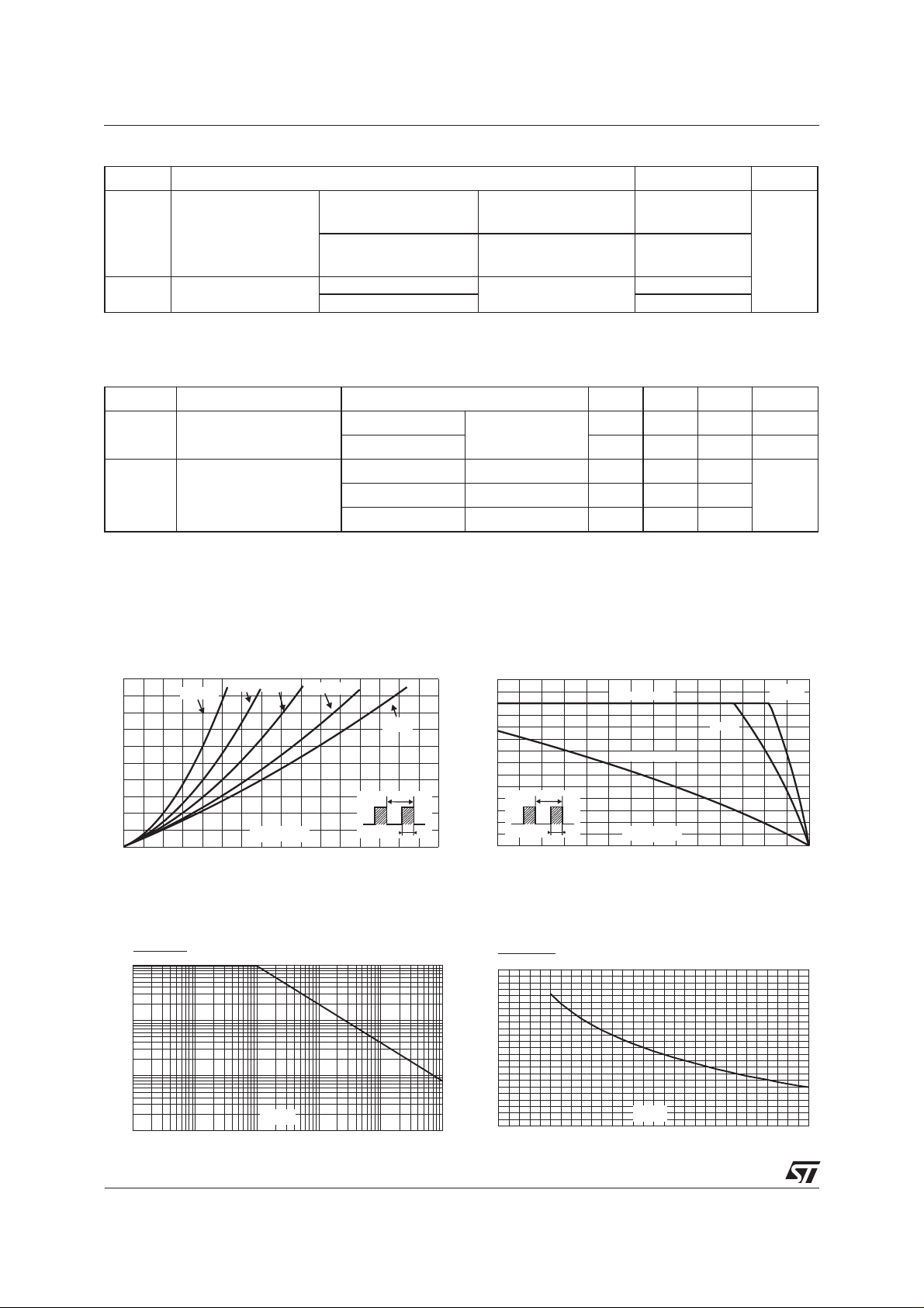
To evaluate the conduction losses use the following equation:
P=0.48xI
Fig. 1: Average forward power dissipation
versus average forward current (per diode).
PF(av)(W)
25
20
15
10
5
0
0 5 10 15 20 25 30 35 40
Fig. 3: Normalized avalanche power derating
versus pulse duration.
P(t)
ARM p
P (1µs)
ARM
1
0.1
0.01
0.001
+ 0.005 I
F(AV)
δ = 0.05
0.10.01 1
δ = 0.1
F2(RMS)
δ = 0.2
IF(av) (A)
t (µs)
p
δ = 0.5
δ = 1
T
=tp/T
δ
10 100 1000
tp
Fig. 2: Average current versus ambient
temperature (δ=0.5, per diode).
IF(av)(A)
35
30
25
20
15
10
5
0
0 25 50 75 100 125 150 175
Fig. 4: Normalized avalanche power derating
versus junction temperature.
P(t)
P (25°C)
ARM
1.2
1
0.8
0.6
0.4
0.2
0
0 25 50 75 100 125 150
=tp/T
δ
ARM p
Rth(j-a)=Rth(j-c)
TOP-3I
Rth(j-a)=10°C/W
T
tp
Tamb(°C)
T (°C)
j
SOT-93
TO-247
2/5
 Loading...