

®
HIGH VOLTAGE POWER SCHOTTKY RECTIFIER
MAIN PRODUCT CHARACTERISTIC S
I
F(AV)
V
RRM
Tj (max) 175 °C
(max) 0.61 V
V
F
5 A
100 V
STPS5H100B/-1
K
A
NC
FEATURES AND BENEFITS
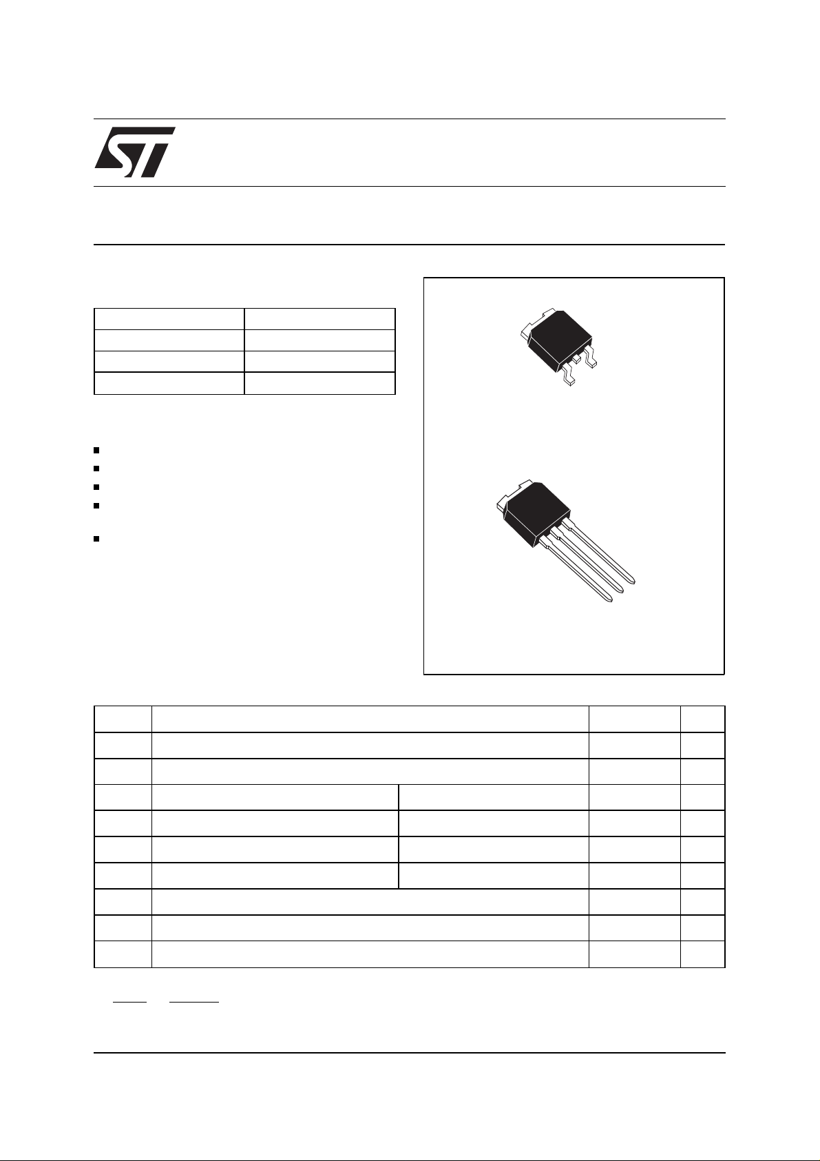
DPAK
STPS5H100B
NEGLIGIBLE SWITCHING LOSSES
HIGH JUNCTION TEMPERATURE CAPABILITY
LOW LEAKAGE CURRE NT
K
GOOD TRADE OFF BETWEEN LEAKAGE
CURRENT AND FORWARD VOLTA GE DROP
AVALANCHE R ATE D
DESCRIPTION
Schottky barrier r ecti fier d esigned fo r hig h frequency miniat ure Switched Mode Power Sup -
A
K
NC
plies such as adaptators and on board DC to
DC converters.
IPAK
STPS5H100B-1
ABSOLUTE RATINGS
(limiting values)
Symbol Parameter Value Unit
V
RRM
I
F(RMS)
I
F(AV)
Repetitive peak reverse voltage 100 V
RMS forward current 10 A
Average forward current Tc = 165°C δ = 0.5 5 A
I
FSM
I
RRM
I
RSM
T
Surge non repetitive forward current tp = 10 ms sinusoidal 75 A
Repetitive peak reverse current tp = 2 µs square F = 1kHz 1 A
Non repetitive peak reverse current tp = 100 µs square 2 A
Storage temperature range - 65 to + 175°C
stg
Tj Maximum operating junction temperature * 175 °C
dV/dt Critical rate of rise of reverse voltage 10000 V/µs
dPtot
* :
July 1999 - Ed: 4B
dTj
<
1
Rth(j−a
thermal runaway condition for a diode on its own heatsink
)
1/5
STPS5H100B/-1
THERMAL RESISTANCES
Symbol Parameter Value Unit
R
th (j-c)
Junction to case 2.5
STATIC ELECTRICAL CHARACTE RISTICS
Symbol Parameter Tests Conditions Min. Typ. Max. Unit
°
C/W
* Reverse leakage current Tj = 25°CV
I
R
= V
R
Tj = 125°C1.34.5mA
** Forward voltage drop Tj = 25°CI
V
F
Tj = 125°CI
Tj = 25°CI
Tj = 125°CI
Pulse test : * tp = 5 ms, δ < 2%
** tp = 380 µs, δ < 2%
To evaluate the maximum conduction losses use the fol lowing equa tion :
P = 0.51 x I
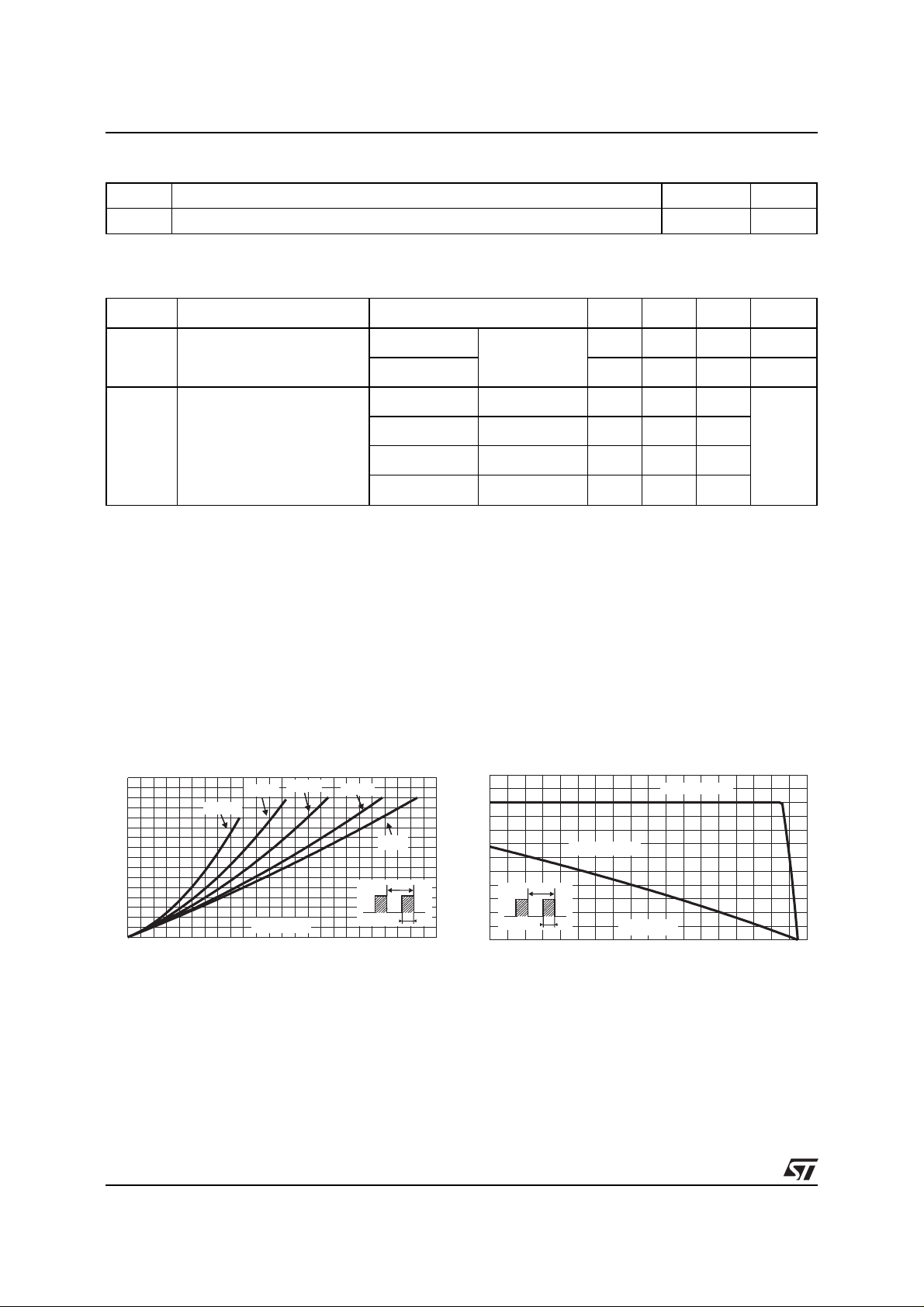
Fig. 1:
+ 0.02 x I
F(AV)
F2(RMS)
Average forward power dissipation versus
average forward current.
PF(av)(W)
4.0
3.5
3.0
2.5
2.0
1.5
1.0
0.5
0.0
0.0 0.5 1.0 1.5 2.0 2.5 3.0 3.5 4.0 4.5 5.0 5.5 6.0
δ = 0.05
δ = 0.1
IF(av) (A)
δ = 0.2
δ = 0.5
δ
=tp/T
δ = 1
T
tp
= 5 A 0.73 V
F
= 5 A 0.57 0.61
F
= 10 A 0.85
F
= 10 A 0.66 0.71
F
Fig. 2:
temperature (δ=0.5).
IF(av)(A)
6
5
4
3
2
1
=tp/T
δ
0
0 20 40 60 80 100 120 140 160 180
RRM
3.5
µ
A
Average forward current versus ambient
Rth(j-a)=Rth(j-c)
Rth(j-a)=80°C/W
T
tp
Tamb(°C)
2/5

STPS5H100B/-1
Fig. 3:
Non repetitive surge peak forward current
versus overload duration (maximum values).
IM(A)
120
110
100
90
80
70
Tc=50°C
60
50
40
30
I
M
20
10
0
1E-3 1E-2 1E-1 1E+0
Fig. 5:
t
δ
=0.5
t(s)
Reverse leakage current versus reverse
Tc=75°C
Tc=125°C
voltage applied.
IR(µA)
5E+3
1E+3
1E+2
Tj=125°C
Fig. 4:
Relative variation of thermal impedance
junction to case versus pulse duration.
Zth(j-c)/Rth(j-c)
1.0
0.8
δ = 0.5
0.6
δ = 0.2
0.4
δ = 0.1
0.2
Single pulse
tp(s)
0.0
1E-3 1E-2 1E-1 1E+0
Fig. 6:
Junction capacitance versus reverse
δ
=tp/T
T
tp
voltage applied (typical values).
C(pF)
1000
F=1MHz
Tj=25°C
1E+1
1E+0
1E-1
1E-2
0 102030405060708090100
Fig. 7:
Forward voltage drop versus forward cur-
Tj=25°C
VR(V)
rent (maximum values).
IFM(A)
50.0
10.0
1.0
0.1
0.0 0.2 0.4 0.6 0.8 1.0 1.2 1.4 1.6
Tj=125°C
Tj=25°C
VFM(V)
100
VR(V)
10
1 10 100
Fig. 8:
Thermal resistance junction to ambient
versus copper surface under tab (Epoxy printed
circuit board FR4, copper thickness: 35µm)
(DPAK).
Rth(j-a) (°C/W)
100
90
80
70
60
50
40
30
20
10
0
0 2 4 6 8 10 12 14 16 18 20
S(Cu) (cm²)
3/5

STPS5H100B/-1
PACKAGE MEC HANICAL D ATA
DPAK
DIMENSIONS
REF.
Millimeters Inches
Min. Max Min. Max.
A 2.20 2.40 0.086 0.094
A1 0.90 1.10 0.035 0.043
A2 0.03 0.23 0.001 0.009
B 0.64 0.90 0.025 0.035
B2 5.20 5.40 0.204 0.212
C 0.45 0.60 0.017 0.023
C2 0.48 0.60 0.018 0.023
D 6.00 6.20 0.236 0.244
E 6.40 6.60 0.251 0.259
G 4.40 4.60 0.173 0.181
H 9.35 10.10 0. 368 0.397
L2 0.80 typ. 0.031 typ.
L4 0.60 1.00 0.023 0.039
V2 0° 8° 0° 8°
FOOT PRINT
(in millimeters)
6.7
6.7
3
3
1.61.6
2.32.3
4/5

PACKAGE ME CHANICAL D AT A
IPAK
E
B2
H
L1
L
B6
G
L2
B3
B
V1
B5
A1
C2
STPS5H100B/-1
DIMENSIONS
REF.
A 2.2 2.4 0.086 0.094
A
A1 0.9 1.1 0.035 0.043
A3 0.7 1.3 0.027 0.051
B 0.64 0.9 0.025 0.035
B2 5.2 5.4 0.204 0.212
B3 0.85 0.033
B5 0.3 0.035
D
B6 0.95 0.037
C 0.45 0.6 0.017 0.023
C2 0.48 0.6 0.019 0.023
D 6 6.2 0.236 0.244
E 6.4 6.6 0.252 0.260
G 4.4 4.6 0.173 0.181
C
A3
H 15.9 16.3 0.626 0.641
L 9 9.4 0.354 0.370
L1 0.8 1.2 0.031 0.047
L2 0.8 1 0.031 0.039
V1 10° 10°
Millimeters Inches
Min. Typ. Max. Min. Typ. Max.
Ordering type Marking Package Weight Base qty Delivery mode
STPS5H100B S5H100 DPAK 0.30g 75 Tube
STPS5H100B-TR S5H100 DPAK 0.30g 2500 Tape & reel
STPS5H100B-1 S5H100 IP AK 0.35g 75 Tube
Epoxy meets UL94,V0
Information furnished is believed to be accurate and reliable. However, STMicroelectronics assumes no responsibility for the conseq ue nces o f
use of such information nor for any infringement of patents or other rights of third parties which may result from its use. No license is granted by
implication or otherwi se un der any pat ent or patent r ights of STM icroele ctronics. Specifica tions m entioned i n this pub lication are subj ect to
change without notice. This publication supersedes and replaces all information previously supplied.
STMicroelectronics products are not authorized for us e as critical components in life support devices or systems without express writ ten approval of STMicroelectronics.
The ST logo is a registered trademark o f STMicroelectron ics
© 1999 STMicroelectronics - Printed in Italy - All rights reserved.
STMicroelectronics GROUP OF COMPANIES
Australia - Brazil - China - Finland - France - Germany - Hong Kong - India - Italy - Japan - Malaysia
Malta - Morocco - Singapore - Spain - Sweden - Switzerland - United Kingdom - U.S.A.
http://www.st.com
5/5
 Loading...