

ST STPS40L45C-Y User Manual
Features
■ Low forward voltage drop meaning very small
conduction losses
■ Low switching losses allowing high frequency
operation
■ Avalanche capability specified
■ AEC-Q101 qualified
Description
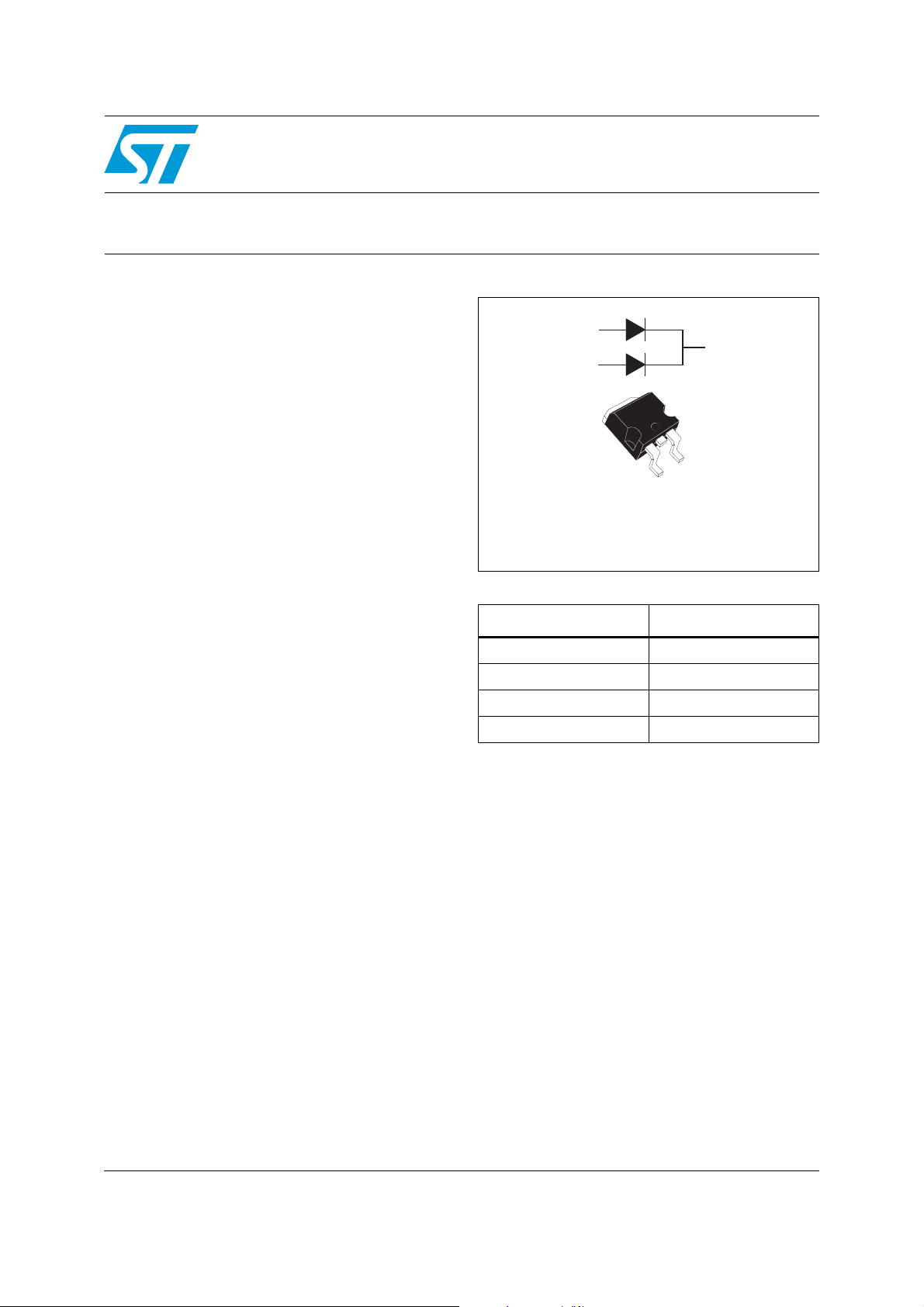
Dual center tap Schottky barrier rectifier designed
for high frequency switched mode power supplies
and DC to DC converters.
Packaged in D²PAK, this device is intended for
use in low voltage, high frequency inverters, freewheeling and polarity protection for automotive
applications.
STPS40L45C-Y
Automotive power Schottky rectifier
Datasheet − production data
A1
K
A2
K
A2
A1
D²PAK
STPS40L45CGY
’
Table 1. Device summary
Symbol Value
I
F(AV)
V
RRM
(max) 150 °C
T
j
V
(max) 0.49 V
F
2 x 20 A
45 V
June 2012 Doc ID 023224 Rev 1 1/7
This is information on a product in full production.
www.st.com
7

Characteristics STPS40L45C-Y
1 Characteristics
Table 2. Absolute ratings (limiting values, per diode)
Symbol Parameter Value Unit
V
I
F(RMS)
I
F(AV)
I
FSM
I
RRM
I
RSM
P
T
Repetitive peak reverse voltage 45 V
RRM
Forward rms current 30 A
Average forward current
=130 °C
T
c
δ = 0.5
per diode
per device
Surge non repetitive forward current tp = 10 ms sinusoidal 230 A
Repetitive peak reverse current tp = 2 µs square F = 1 kHz 2 A
Non repetitive peak reverse current tp = 100 µs square 3 A
Repetitive peak avalanche power tp = 1 µs Tj = 25 °C 8100 W
ARM
Storage temperature range -65 to + 150 °C
stg
T
Operating junction temperature
j
(1)
-40 to + 150 °C
20
40
dV/dt Critical rate of rise of reverse voltage 10000 V/µs
<
Rth(j-a)
1
dPtot
1. condition to avoid thermal runaway for a diode on its own heatsink
dTj
Table 3. Thermal resistances
Symbol Parameter Value Unit
R
R
th (j-c)
th(c)
Junction to case
Per diode
To ta l
Coupling 0.1 °C/W
1.5
0.8
°C/W
A
When the diodes 1 and 2 are used simultaneously :
ΔT
(diode 1) = P(diode1) x R
j
Table 4. Static electrical characteristics (per diode)
(Per diode) + P(diode 2) x R
th(j-c)
Symbol Parameter Test conditions Min. Typ. Max. Unit
= 25 °C
T
Reverse leakage
(1)
I
R
current
(1)
V
1. Pulse test: tp = 380 µs, δ < 2%
Forward voltage drop
F
j
= 125 °C 140 280 mA
T
j
= 25 °C IF = 20 A 0.53
T
j
T
= 125 °C IF = 20 A 0.42 0.49
j
= 25 °C IF = 40 A 0.69
T
j
T
= 125 °C IF = 40 A 0.6 0.7
j
= V
V
R
To evaluate the conduction losses use the following equation:
P = 0.28 x I
2/7 Doc ID 023224 Rev 1
F(AV)
+ 0.0105 I
F2(RMS)
RRM
th(c)
.
0.6 mA
V

STPS40L45C-Y Characteristics
Figure 1. Average forward power dissipation
versus average forward current
(per diode)
P
(W)
F(AV)
16
14
12
10
8
6
4
2
0
0 2 4 6 8 1012141618202224
δ = 0.05
δ = 0.1
I
F(AV)
δ = 0.2
(A)
δ = 0.5
δ = tp/T
δ = 1
T
t
p
Figure 3. Normalized avalanche power
derating versus pulse duration
P(tp)
ARM
P (1 µs)
ARM
1
0.1
0.01
t (µs)
0.001
0.10.01 1
10 100 1000
p
Figure 2. Average forward current versus
ambient temperature
(
δ = 0.5, per diode)
I
(A)
F(AV)
22
20
18
16
14
12
10
8
6
4
2
0
T
δ = tp/T
0 25 50 75 100 125 150
t
p
R
th(j-a)
R
th(j-a)
= 15 °C/W
T
amb
= R
th(j-c)
(°C)
Figure 4. Normalized avalanche power
derating versus junction
temperature
P(T)
ARM j
P (25 °C)
ARM
1.2
1
0.8
0.6
0.4
0.2
T (°C)
0
25 50 75 100 125
j
150
Figure 5. Non repetitive surge peak forward
current versus overload duration
(maximum values, per diode)
IM(A)
250
225
200
175
150
125
100
75
50
25
0
1E-3 1E-2 1E-1 1E+0
t(s)
Tc = 25 °C
Tc = 75 °C
Tc = 125 °C
Doc ID 023224 Rev 1 3/7
Figure 6. Relative variation of thermal
impedance junction to case versus
pulse duration
Z
th(j-c)/Rth(j-c)
1.0
0.8
δ
= 0.5
0.6
0.4
δ
= 0.2
δ
= 0.1
0.2
0.0
1E-4
Single pulse
tp(s)
1E-3 1E-2 1E-1 1E+0
δ = tp/T
T
t
p
 Loading...