

®
STPS40L40CT/CW
LOW DROP POWER SCHOTTKY RECTIFIER
MAIN PRODUCTS CHARACTERISTICS
I
F(AV)
V
RRM
2x20A
40 V
Tj (max) 150 °C
(max) 0.49 V
V
F
FEATURES AND BENEFITS
LOW FORWARD VOLTAGE DROP MEANING
n
VERY SMALL CONDUCTION LOSSES
LOW DYNAMIC LOSSES AS A RESULT OF
n
THE SCHOTTKY BARRIER
AVALANCHE CAPABILITY SPECIFIED
n
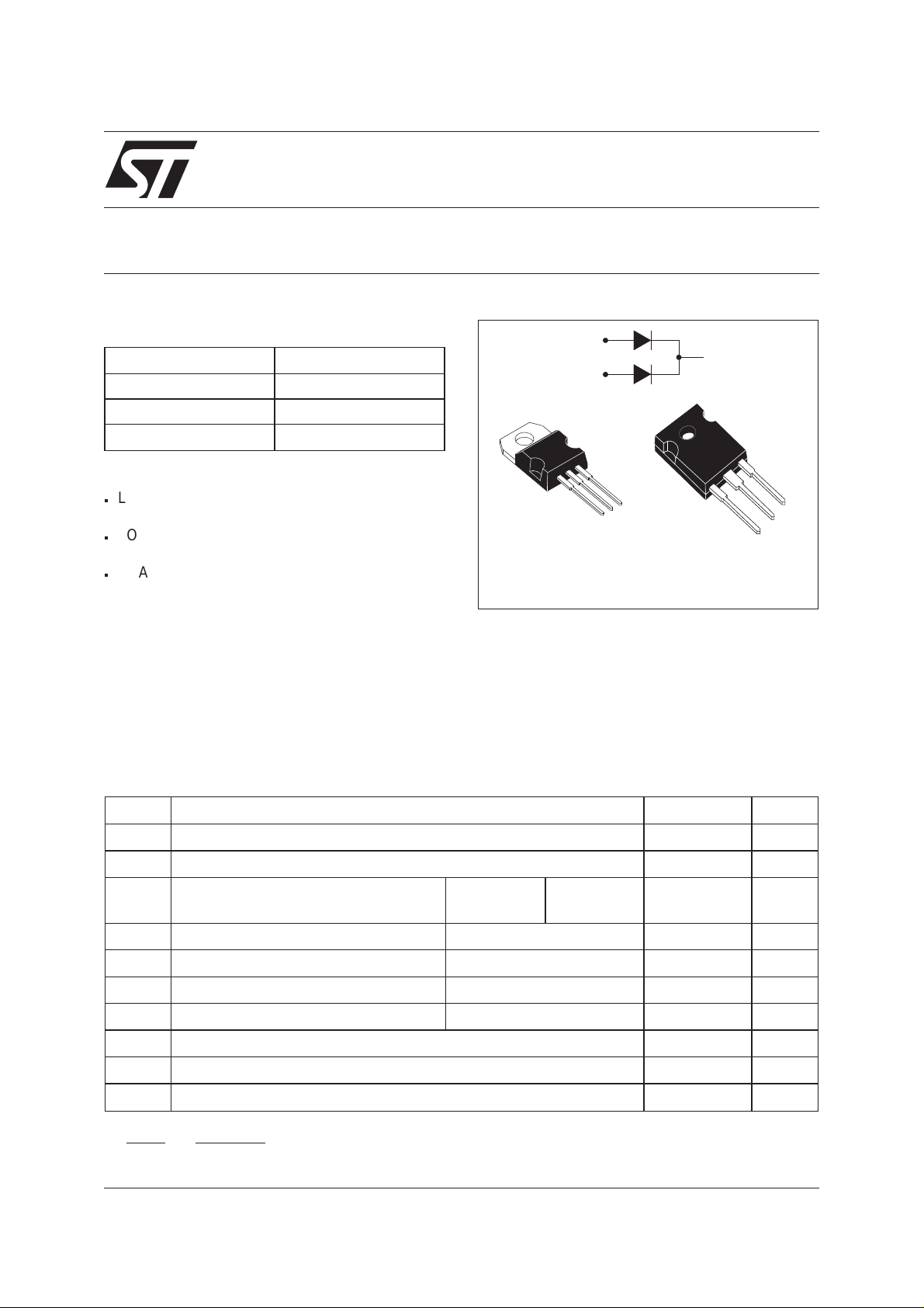
DESCRIPTION
Dual center tap Schottky barrier rectifier designed
for highfrequencySwitchedModePowerSupplies
and DC to DC converters.
Packaged in TO-220ABand TO-247 this device is
intended for use in low voltage, high frequency
inverters, free-wheeling and polarity protection
applications.
ABSOLUTE RATINGS (limiting values, per diode)
A1
A2
A1
TO-220AB
STPS40L40CT
K
A2
K
A2
K
A1
TO-247
STPS40L40CW
Symbol Parameter Value Unit
V
RRM
I
F(RMS)
I
F(AV)
I
FSM
I
RRM
I
RSM
P
ARM
T
stg
Tj
dV/dt
dPtot
*:
Repetitive peak reverse voltage
RMS forward current
Average forward current Tc = 130°C
Surge non repetitive forward current tp = 10 ms Sinusoidal
Repetitive peak reverse current tp=2µs square F = 1kHz
Non repetitive peak reverse current tp = 100 µs square
Repetitive peak avalanche power tp = 1µs Tj = 25°C
Storage temperature range
Maximum operating junction temperature *
Critical rate of rise of reverse voltage
<
dTj Rth j a
July 2003 - Ed: 7A
Per diode
δ = 0.5
Per device
thermal runawaycondition for a diode on its own heatsink
−1()
40 V
30 A
20
40
230 A
2A
3A
8100 W
-65 to+150 °C
150 °C
10000 V/µs
A
1/5
STPS40L40CT/CW
THERMAL RESISTANCES
Symbol Parameter Value Unit
R
th (j-c)
Junction to case
Per diode
Total
R
th(c)
Coupling
When the diodes 1 and 2 areused simultaneously :
∆ Tj(diode 1) = P(diode1) x R
(Per diode) + P(diode 2) x R
th(j-c)
th(c)
STATIC ELECTRICAL CHARACTERISTICS (per diode)
Symbol Parameter Tests Conditions Min. Typ. Max. Unit
*
I
R
Reverse leakage current Tj = 25°CV
R=VRRM
Tj = 100°C
V
*
F
Forward voltage drop Tj = 25°CI
Tj = 125°CI
Tj=25°CI
Tj = 125°CI
=20A
F
=20A
F
=40A
F
=40A
F
Pulse test:*tp=380µs,δ<2%
To evaluate the conduction losses use the following equation :
P=0.28xI
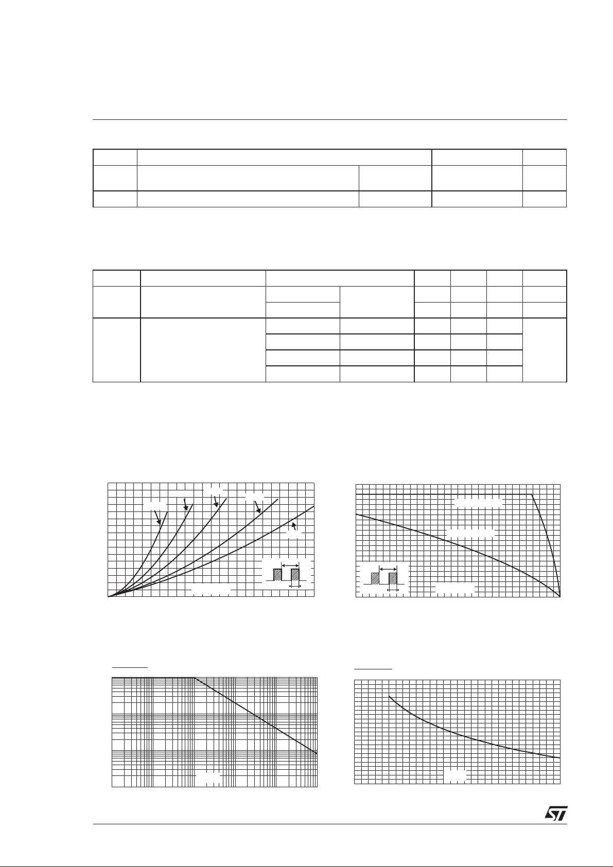
Fig. 1: Average forward power dissipation versus
average forward current (per diode).
F(AV)
+ 0.0105 I
F2(RMS)
Fig. 2: Average current versus ambient
temperature (δ = 0.5, per diode).
1.5
°C/W
0.8
0.1 °C/W
0.8 mA
30 70 mA
0.53 V
0.42 0.49
0.69
0.6 0.7
PF(av)(W)
16
14
12
δ = 0.05
10
8
6
4
2
0
024681012141618202224
δ = 0.1
δ = 0.2
IF(av) (A)
δ = 0.5
δ
=tp/T
δ = 1
T
tp
Fig. 3: Normalized avalanche power derating
versus pulse duration.
P(t)
ARM p
P (1µs)
ARM
1
0.1
0.01
t (µs)
0.001
0.10.01 1
p
10 100 1000
IF(av)(A)
22
20
18
16
14
12
10
8
6
4
2
0
0 25 50 75 100 125 150
δ
=tp/T
T
tp
Rth(j-a)=Rth(j-c)
Rth(j-a)=15°C/W
Tamb(°C)
Fig. 4: Normalized avalanche power derating
versus junction temperature.
P(t)
ARM p
P (25°C)
ARM
1.2
1
0.8
0.6
0.4
0.2
0
0 25 50 75 100 125 150
T (°C)
j
2/5

STPS40L40CT/CW
Fig. 5: Non repetitive surge peak forward current
versus overload duration (maximum values, per
diode).
IM(A)
250
225
200
175
150
125
100
75
I
M
50
25
0
1E-3 1E-2 1E-1 1E+0
t
δ
=0.5
t(s)
Tc=25°C
Tc=75°C
Tc=125°C
Fig. 7: Reverse leakage current versus reverse
voltage applied (typical values, per diode).
IR(mA)
5E+2
1E+2
Tj=150°C
Tj=125°C
Fig. 6: Relative variation of thermal impedance
junction to case versus pulse duration.
Zth(j-c)/Rth(j-c)
1.0
0.8
δ = 0.5
0.6
0.4
δ = 0.2
δ
=tp/T
T
tp
δ = 0.1
0.2
Single pulse
0.0
1E-4 1E-3 1E-2 1E-1 1E+0
tp(s)
Fig. 8: Junction capacitance versus reverse
voltage applied (typical values, per diode).
C(nF)
5.0
F=1MHz
Tj=25°C
1E+1
Tj=75°C
1E+0
1E-1
1E-2
0 5 10 15 20 25 30 35 40
Tj=25°C
VR(V)
Fig. 9: Forward voltage drop versus forward
current (maximum values, per diode).
IFM(A)
200
100
Typical values
Tj=150°C
Tj=125°C
10
1
0.0 0.2 0.4 0.6 0.8 1.0 1.2 1.4 1.6
Tj=75°C
Tj=25°C
VFM(V)
1.0
0.1
12 51020 50
VR(V)
3/5

STPS40L40CT/CW
PACKAGE MECHANICAL DATA
TO-220AB
DIMENSIONS
L2
F2
F1
F
G1
H2
Dia
G
L5
L9
L6
L4
REF.
A
C
A 4.40 4.60 0.173 0.181
Millimeters Inches
Min. Max. Min. Max.
C 1.23 1.32 0.048 0.051
L7
D 2.40 2.72 0.094 0.107
E 0.49 0.70 0.019 0.027
F 0.61 0.88 0.024 0.034
F1 1.14 1.70 0.044 0.066
F2 1.14 1.70 0.044 0.066
D
G 4.95 5.15 0.194 0.202
G1 2.40 2.70 0.094 0.106
H2 10 10.40 0.393 0.409
L2 16.4 typ. 0.645typ.
L4 13 14 0.511 0.551
M
E
L5 2.65 2.95 0.104 0.116
L6 15.25 15.75 0.600 0.620
L7 6.20 6.60 0.244 0.259
L9 3.50 3.93 0.137 0.154
M 2.6 typ. 0.102 typ.
Diam. 3.75 3.85 0.147 0.151
n
COOLING METHOD : C
n
RECOMMENDED TORQUE VALUE : 0.55M.N
n
MAXIMUM TORQUE VALUE : 0.70 M.N
4/5

PACKAGE MECHANICAL DATA
TO-247
STPS40L40CT/CW
DIMENSIONS
V
REF.
Millimeters Inches
Min. Typ. Max. Min. Typ. Max.
V
Dia.
A 4.85 5.15 0.191 0.203
D 2.20 2.60 0.086 0.102
E 0.40 0.80 0.015 0.031
F 1.00 1.40 0.039 0.055
F1 3.00 0.118
H
A
F2 2.00 0.078
F3 2.00 2.40 0.078 0.094
L5
F4 3.00 3.40 0.118 0.133
G 10.90 0.429
L
L4L2
H 15.45 15.75 0.608 0.620
L 19.85 20.15 0.781 0.793
L1 3.70 4.30 0.145 0.169
F1
V2
F(x3)
G
= =
F4
F3
F2
L3
L1
D
ME
L2 18.50 0.728
L3 14.20 14.80 0.559 0.582
L4 34.60 1.362
L5 5.50 0.216
M 2.00 3.00 0.078 0.118
V5° 5°
V2 60° 60°
Dia. 3.55 3.65 0.139 0.143
n
COOLING METHOD : C
n
RECOMMENDED TORQUE VALUE : 0.8M.N
n
MAXIMUM TORQUE VALUE : 1.0M.N
Ordering type Marking Package Weight Base qty Delivery mode
STPS40L40CT STPS40L40CT TO-220AB 2g 50 Tube
STPS40L40CW STPS40L40CW TO-247 4.4g 30 Tube
n
EPOXY MEETS UL94,V0
Informationfurnished isbelievedto be accurateand reliable. However,STMicroelectronics assumesnoresponsibility fortheconsequences of
useof suchinformation nor forany infringement ofpatents or otherrights ofthirdparties whichmay result fromits use. Nolicense is grantedby
implication or otherwise under any patent or patent rights of STMicroelectronics. Specifications mentioned in this publication are subject to
change withoutnotice. This publication supersedes and replaces all information previously supplied.
STMicroelectronics products are not authorized for use as critical components in life support devices or systems without express written
approval ofSTMicroelectronics.
The ST logo is a registered trademark of STMicroelectronics
© 2003 STMicroelectronics - Printed in Italy - All rights reserved.
STMicroelectronics GROUP OF COMPANIES
Australia - Brazil - Canada - China - Finland - France - Germany
Hong Kong - India - Israel - Italy - Japan - Malaysia - Malta - Morocco - Singapore
Spain - Sweden - Switzerland - United Kingdom - United States.
http://www.st.com
5/5
 Loading...