

Main product characteristics
I
F(AV)
V
RRM
T
(max) 150° C
j
(max) 0.57 V
V
F
3 A
40 V
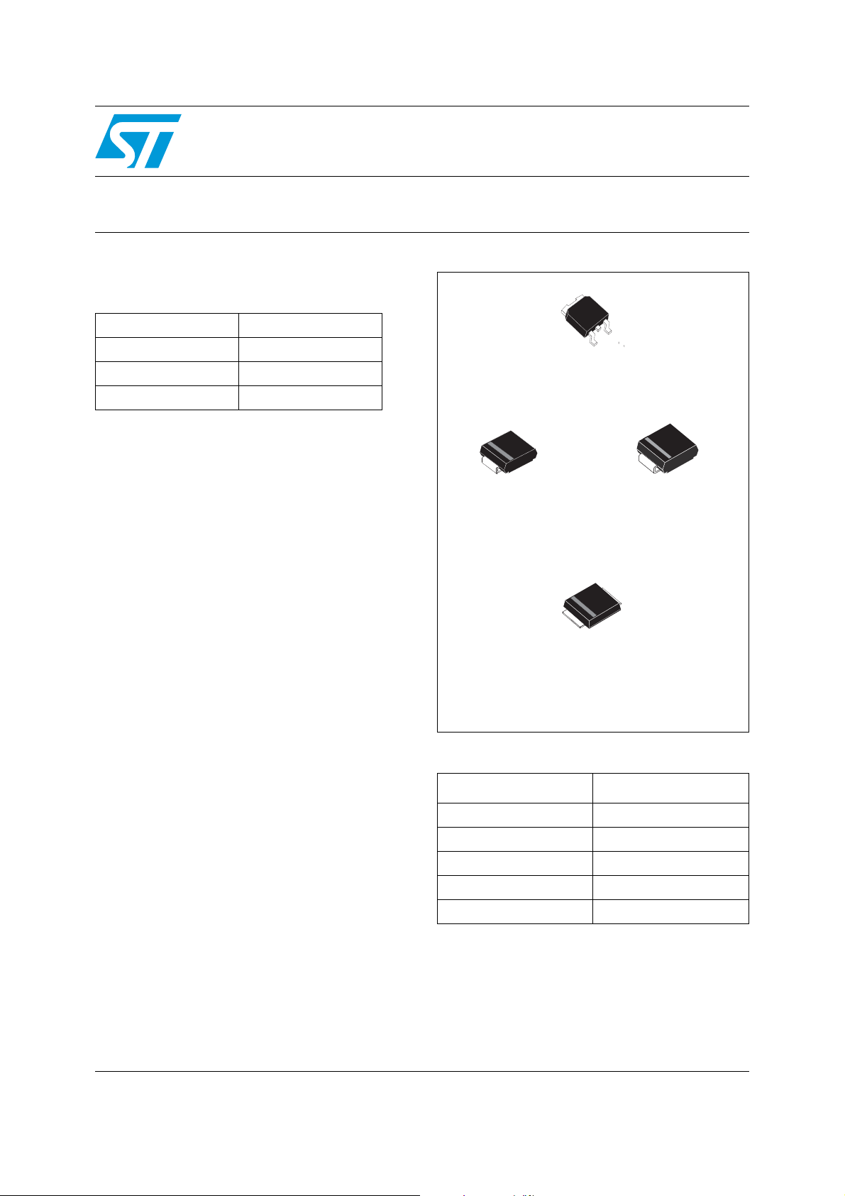
STPS340
Power Schottky rectifier
K
A
NC
DPAK
STPS340B
Features and Benefits
■ Very small conduction losses
■ Negligible switching losses
■ Low forward voltage drop
■ Low thermal resistance
■ Extremely fast switching
■ Surface mounted device
■ Avalanche capability specified
Description
Single chip Schottky rectifier suited for switch
mode power supplies and high frequency DC to
DC converters.
Packaged in DPAK, SMC, SMB, and low profile
SMB, this device is intended for use in low and
medium voltage operation, high frequency
inverters, free wheeling and polarity protection
applications where low switching losses are
required.
A
K
SMB
STPS340U
K
SMB flat
STPS340UF
Order codes
Part Number Marking
STPS340U U34
STPS340S S34
STPS340B S340
A
K
SMC
STPS340S
A
STPS340B-TR S340
STPS340UF FU34
February 2007 Rev 9 1/11
www.st.com
11
Characteristics STPS340
1 Characteristics
Table 1. Absolute Ratings (limiting values)
Symbol Parameter Value Unit
V
I
F(RMS)
I
F(AV)
I
P
T
1. condition to avoid thermal runaway for a diode on its own heatsink
Table 2. Thermal resistance
Repetitive peak reverse voltage 40 V
RRM
RMS forward current DPAK 6 A
T
= 135° C δ = 0.5 DPAK
c
Average forward current
Surge non repetitive forward current tp =10 ms sinusoidal 75 A
FSM
Repetitive peak avalanche power tp = 1 µs Tj = 25° C 1300 W
ARM
Storage temperature range -65 to + 150 °C
stg
Operating junction temperature
T
j
dPtot
--------------dTj
1
--------------------------
<
Rth j a–()
= 105° C δ = 0.5 SMB/SMC
L
T
= 115° C δ = 0.5 SMB flat
L
(1)
3AT
150 °C
Symbol Parameter Value Unit
SMB 25
R
th(j-l)
Junction to lead
°C/WSMB flat 15
SMC 20
th(j-c)
Junction to case DPAK 5.5 °C/W
R
Table 3. Static electrical characteristics
Symbol Parameter Test Conditions Min. Typ. Max. Unit
= 25° C
T
(1)
I
V
1. Pulse test: tp = 380 µs, δ < 2%
Reverse leakage current
R
(1)
Forward voltage drop
F
j
= 125° C 2 10 mA
T
j
= 25° C
T
j
T
= 125° C 0.52 0.57
j
= 25° C
T
j
T
= 125° C 0.63 0.72
j
To evaluate the conduction losses use the following equation:
P = 0.42 x I
2/11
F(AV)
+ 0.050 I
F2(RMS)
V
R
= 3 A
I
F
= 6 A
I
F
= V
20 µA
RRM
0.63
V
0.84
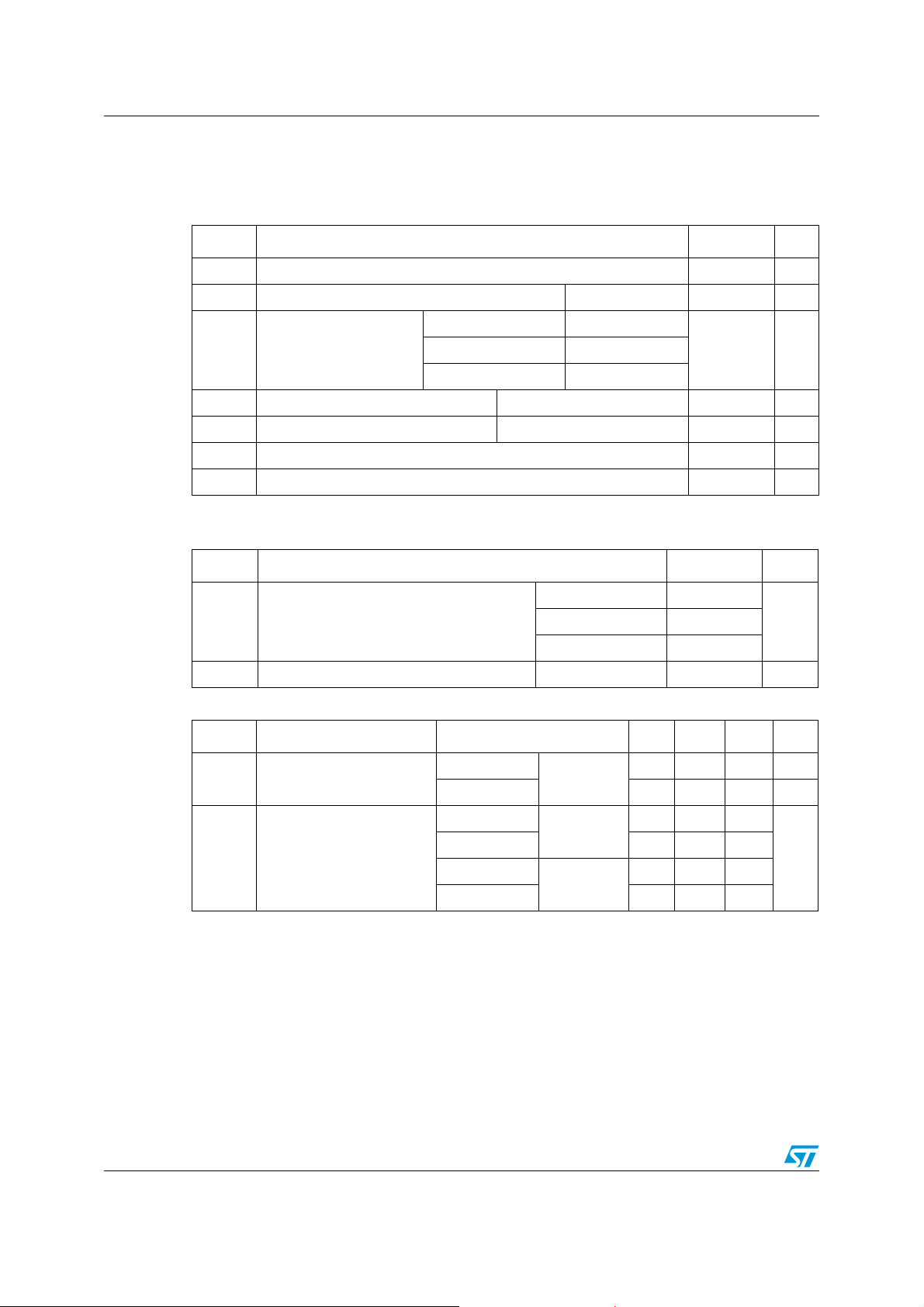
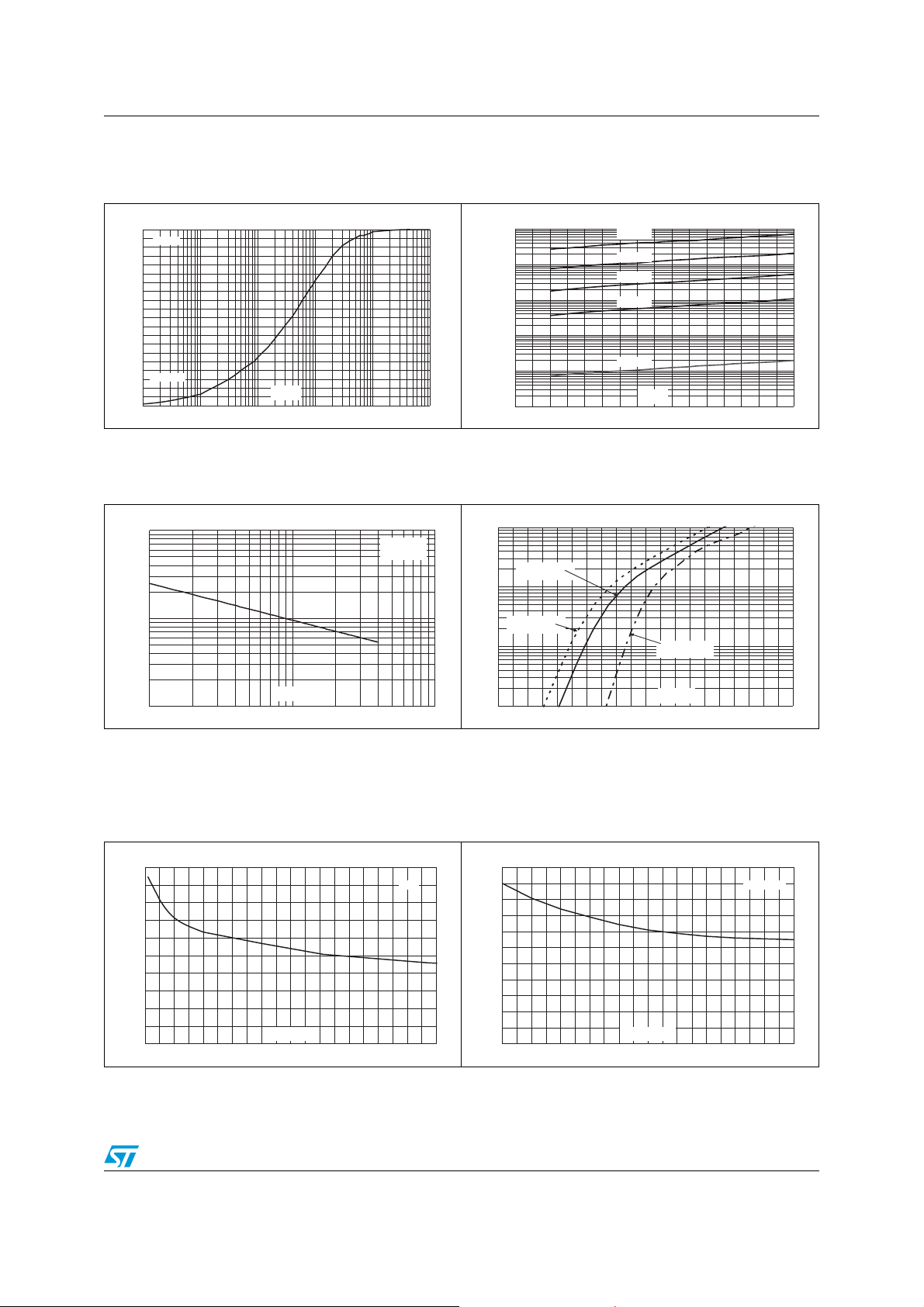
STPS340 Characteristics
Figure 1. Average forward power dissipation
versus average forward current (per
diode)
P (W)
F(AV)
2.5
2.0
1.5
1.0
0.5
0.0
0.0 0.5 1.0 1.5 2.0 2.5 3.0 3.5 4.0
δ = 0.05
δ = 0.1
δ = 0.2
I (A)
F(AV)
δ = 0.5
δ
=tp/T
δ = 1
T
tp
Figure 3. Average forward current versus
ambient temperature (δ = 0.5, per
diode) (SMB flat)
I (A)
F(AV)
3.5
3.0
2.5
2.0
1.5
1.0
0.5
0.0
0 25 50 75 100 125 150
δ
=tp/T
T
tp
R=R
th(j-a) th(j-l)
T (°C)
amb
SMB flat
R =40°C/W
th(j-a)
. S =2.5 cm
CU
2
Figure 5. Non repetitive surge peak forward
current versus overload duration
(maximum values) (SMB)
I (A)
M
10
9
8
7
6
5
4
3
2
IM
1
0
1.E-03 1.E-02 1.E-01 1.E+00
δ=0.5
t
t(s)
SMB
T =25°C
a
T =75°C
a
T =125°C
a
Figure 2. Average forward current versus
ambient temperature (δ = 0.5, per
diode) (DPAK / SMB / SMC)
I (A)
F(AV)
3.5
3.0
2.5
R =65°C/W
δ
=tp/T
th(j-a)
T
tp
2.0
1.5
1.0
0.5
0.0
0 25 50 75 100 125 150
R=R
th(j-a) th(j-l)
T (°C)
amb
DPAK
SMB / SMC
Figure 4. Non repetitive surge peak forward
current versus overload duration
(maximum values) (DPAK)
I (A)
M
60
50
40
30
20
IM
10
0
1.E-03 1.E-02 1.E-01 1.E+00
δ=0.5
t
t(s)
DPAK
T =25°C
c
T =75°C
c
T =125°C
c
Figure 6. Non repetitive surge peak forward
current versus overload duration
(maximum values) (SMC)
I (A)
M
12
11
10
9
8
7
6
5
4
3
IM
2
1
0
1.E-03 1.E-02 1.E-01 1.E+00
δ=0.5
t
t(s)
SMC
T =25°C
a
T =75°C
a
T =125°C
a
3/11
Characteristics STPS340
Figure 7. Non repetitive surge peak forward
current versus overload duration
(maximum values) SMB flat
I (A)
M
25
20
15
10
5
IM
t
0
1.E-03 1.E-02 1.E-01 1.E+00
δ=0.5
t(s)
SMB flat
T =25°C
L
T =75°C
L
T =125°C
L
Figure 9. Normalized avalanche power
derating versus junction
temperature
P(t)
ARM p
P (25°C)
ARM
1.2
1
0.8
0.6
0.4
0.2
0
25 50 75 100 125 150
T (°C)
j
Figure 11. Relative variation of thermal
impedance junction to ambient
versus pulse duration (SMB)
Z/R
th(j-a) th(j-a)
1.0
SMB
0.9
0.8
0.7
0.6
0.5
0.4
0.3
0.2
Single pulse
0.1
0.0
1.E-02 1.E-01 1.E+00 1.E+01 1.E+02 1.E+03
t (s)
p
δ
=tp/T
T
tp
Figure 8. Normalized avalanche power
derating versus pulse duration
P(t)
ARM p
P (1µs)
ARM
1
0.1
0.01
t (µs)
0.001
0.10.01 1
p
10 100 1000
Figure 10. Relative variation of thermal
impedance junction to ambient
versus pulse duration (DPAK)
Z/R
th(j-a) th(j-a)
1.0
DPAK
0.9
0.8
0.7
0.6
0.5
0.4
Single pulse
0.3
0.2
0.1
0.0
1.E-03 1.E-02 1.E-01 1.E+00
t (s)
p
δ
T
=tp/T
Figure 12. Relative variation of thermal
impedance junction to ambient
versus pulse duration (SMC)
Z/R
th(j-a) th(j-a)
1.0
SMC
0.9
0.8
0.7
0.6
0.5
0.4
0.3
0.2
Single pulse
0.1
0.0
1.E-02 1.E-01 1.E+00 1.E+01 1.E+02 1.E+03
t (s)
p
δ
T
=tp/T
tp
tp
4/11
STPS340 Characteristics
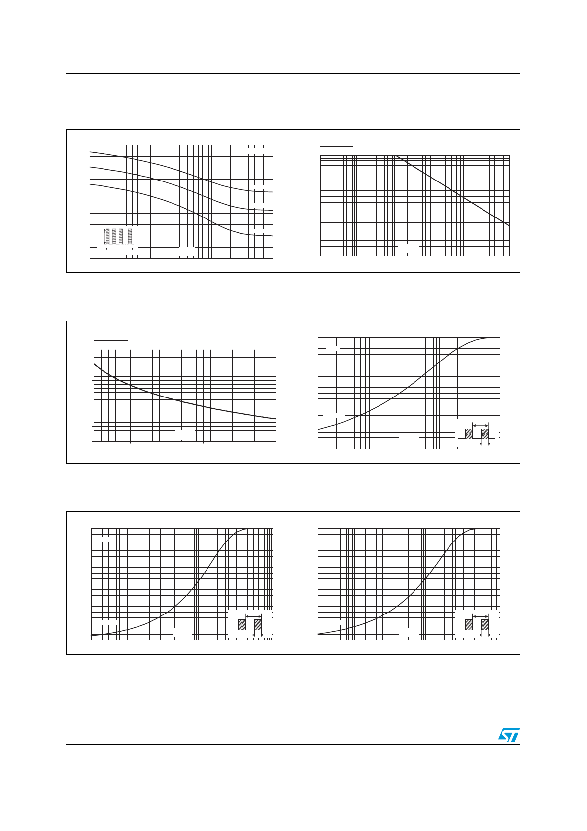
Figure 13. Relative variation of thermal
impedance junction to lead
versus pulse duration - SMB flat
Z/R
th(j-l) th(j-l)
1.0
SMB flat
0.9
0.8
0.7
0.6
0.5
0.4
0.3
0.2
Single pulse
0.1
0.0
1.E-04 1.E-03 1.E-02 1.E-01 1.E+00 1.E+01
t (s)
p
Figure 15. Junction capacitance versus
reverse voltage applied (typical
values)
C(pF)
1000
F=1MHz
V =30mV
OSC RMS
T=25°C
j
Figure 14. Reverse leakage current versus
reverse voltage applied (typical
values)
I (mA)
R
1.E+01
1.E+00
1.E-01
1.E-02
1.E-03
1.E-04
0 5 10 15 20 25 30 35 40
Tj=150°C
Tj=125°C
Tj=100°C
Tj=75°C
Tj=25°C
V (V)
R
Figure 16. Forward voltage drop versus
forward current
I (A)
FM
10
Tj=125°C
(Maximum values)
1
100
V (V)
10
1 10 100
R
Figure 17. Thermal resistance junction to
ambient versus copper surface
under each lead (epoxy printed
board FR4, e
R (°C/W)
th(j-a)
100
90
80
70
60
50
40
30
20
10
0
0.0 0.5 1.0 1.5 2.0 2.5 3.0 3.5 4.0 4.5 5.0
= 35 µm) (DPAK)
CU
S (cm²)
CU
DPAK
Tj=125°C
Tj=125°C
(Typical values)
(Typical values)
0
0
0.0 0.1 0.2 0.3 0.4 0.5 0.6 0.7 0.8 0.9 1.0
Tj=25°C
(Maximum values)
V (V)
FM
Figure 18. Thermal resistance junction to
ambient versus copper surface
under each lead (epoxy printed
board FR4, e
= 35 µm)
CU
(SMB / SMC)
R (°C/W)
th(j-a)
110
100
90
80
70
60
50
40
30
20
10
0
0.0 0.5 1.0 1.5 2.0 2.5 3.0 3.5 4.0 4.5 5.0
S (cm²)
CU
SMB / SMC
5/11

Package Information STPS340
Figure 19. Thermal resistance junction to
ambient versus copper surface
under each lead (epoxy printed
board FR4, e
R (°C/W)
th(j-a)
110
100
90
80
70
60
50
40
30
20
10
0
0.0 0.5 1.0 1.5 2.0 2.5 3.0 3.5 4.0 4.5 5.0
SMB flat
= 35 µm) (SMB flat)
CU
S (cm²)
CU
2 Package Information
● Band indicates cathode on SMB and SMC
● Epoxy meets UL94, V0
Table 4. DPAK dimensions
E
B2
L2
H
L4
B
G
0.60 MIN.
A1
A2
V2
A
C2
D
R
R
C
Dimensions
Ref
Millimeters Inches
Min. Max. Min. Max.
A 2.20 2.40 0.086 0.094
A1 0.90 1.10 0.035 0.043
A2 0.03 0.23 0.001 0.009
B 0.64 0.90 0.025 0.035
B2 5.20 5.40 0.204 0.212
C 0.45 0.60 0.017 0.023
C2 0.48 0.60 0.018 0.023
D 6.00 6.20 0.236 0.244
E 6.40 6.60 0.251 0.259
G 4.40 4.60 0.173 0.181
H 9.35 10.10 0.368 0.397
L2 0.80 typ. 0.031 typ.
L4 0.60 1.00 0.023 0.039
V2 0° 8° 0° 8°
6/11
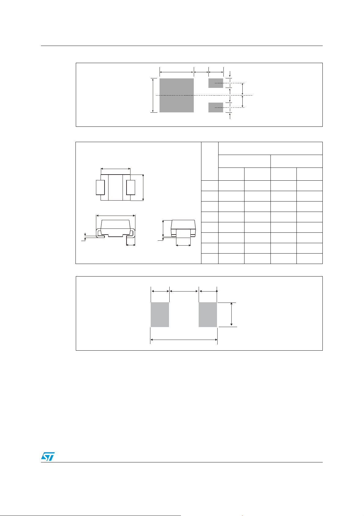
STPS340 Package Information
Figure 20. DPAK footprint dimensions (in millimeters)
1.6
2.3
2.3
1.6
Dimensions
6.7
Table 5. SMB dimensions
6.7 3 3
E1
D
E
A1
C
L
A2
b
Ref.
Figure 21. SMB footprint (dimensions in mm)
1.62
2.60
5.84
1.62
Millimeters Inches
Min. Max. Min. Max.
A1 1.90 2.45 0.075 0.096
A2 0.05 0.20 0.002 0.008
b 1.95 2.20 0.077 0.087
c 0.15 0.40 0.006 0.016
E 5.10 5.60 0.201 0.220
E1 4.05 4.60 0.159 0.181
D 3.30 3.95 0.130 0.156
L 0.75 1.50 0.030 0.059
2.18
7/11
Package Information STPS340
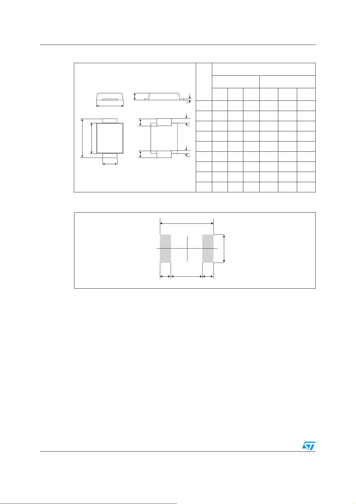
Table 6. SMB Flat dimensions
Dimensions
Ref.
A
D
L
E
E1
c
A 0.90 1.10 0.035 0.043
(1)
b
(1)
c
L2
D 3.30 3.95 0.130 0.156
E 5.10 5.60 0.200 0.220
L
b
E1 4.05 4.60 0.189 0.181
L1
L 0.75 1.50 0.029 0.059
L1 0.40 0.016
L2 0.60 0.024
1. Applies to plated leads
Figure 22. SMB Flat footprint (dimensions in mm)
5.84
Millimeters Inches
Min. Typ. Max. Min. Typ. Max.
1.95 2.20 0.077 0.087
0.15 0.40 0.006 0.016
2.07
1.20 1.203.44
8/11

STPS340 Package Information
Table 7. SMC package mechanical data
Dimensions
Ref
E1
D
A1 1.90 2.45 0.075 0.096
A2 0.05 0.20 0.002 0.008
E
A1
E 7.75 8.15 0.305 0.321
E1 6.60 7.15 0.260 0.281
C
LE2
A2
b
E2 4.40 4.70 0.173 0.185
D 5.55 6.25 0.218 0.246
Figure 23. Foot print dimensions (in millimeters)
1.54
5.03
Millimeters Inches
Min. Max. Min. Max.
b 2.90 3.2 0.114 0.126
c 0.15 0.41 0.006 0.016
L 0.75 1.40 0.030 0.063
1.54
3.15
8.11
In order to meet environmental requirements, ST offers these devices in ECOPACK®
packages. These packages have a lead-free second level interconnect. The category of
second level interconnect is marked on the package and on the inner box label, in
compliance with JEDEC Standard JESD97. The maximum ratings related to soldering
conditions are also marked on the inner box label. ECOPACK is an ST trademark.
ECOPACK specifications are available at: www.st.com.
9/11

Ordering information STPS340
3 Ordering information
Ordering type Marking Package Weight Base qty Delivery mode
STPS340U U34 SMB 0.107 g 2500
STPS340S S34 SMC 0.243 g 2500
STPS340B
S340 DPAK 0.30 g
STPS340B-TR 2500 Tape and reel
STPS340UF FU34 SMB flat 0.50 g 5000 Tape and reel
4 Revision history
Date Revision Description of Changes
Jul-2003 7B Last update.
Feb-2005 8 Layout update. No content change.
08-Feb-2007 9
Tape and reel
75 Tube
Reformatted to current standard. Added ECOPACK
statement. Added SMB flat package.
10/11

STPS340
Please Read Carefully:
Information in this document is provided solely in connection with ST products. STMicroelectronics NV and its subsidiaries (“ST”) reserve the
right to make changes, corrections, modifications or improvements, to this document, and the products and services described herein at any
time, without notice.
All ST products are sold pursuant to ST’s terms and conditions of sale.
Purchasers are solely responsible for the choice, selection and use of the ST products and services described herein, and ST assumes no
liability whatsoever relating to the choice, selection or use of the ST products and services described herein.
No license, express or implied, by estoppel or otherwise, to any intellectual property rights is granted under this document. If any part of this
document refers to any third party products or services it shall not be deemed a license grant by ST for the use of such third party products
or services, or any intellectual property contained therein or considered as a warranty covering the use in any manner whatsoever of such
third party products or services or any intellectual property contained therein.
UNLESS OTHERWISE SET FORTH IN ST’S TERMS AND CONDITIONS OF SALE ST DISCLAIMS ANY EXPRESS OR IMPLIED
WARRANTY WITH RESPECT TO THE USE AND/OR SALE OF ST PRODUCTS INCLUDING WITHOUT LIMITATION IMPLIED
WARRANTIES OF MERCHANTABILITY, FITNESS FOR A PARTICULAR PURPOSE (AND THEIR EQUIVALENTS UNDER THE LAWS
OF ANY JURISDICTION), OR INFRINGEMENT OF ANY PATENT, COPYRIGHT OR OTHER INTELLECTUAL PROPERTY RIGHT.
UNLESS EXPRESSLY APPROVED IN WRITING BY AN AUTHORIZED ST REPRESENTATIVE, ST PRODUCTS ARE NOT
RECOMMENDED, AUTHORIZED OR WARRANTED FOR USE IN MILITARY, AIR CRAFT, SPACE, LIFE SAVING, OR LIFE SUSTAINING
APPLICATIONS, NOR IN PRODUCTS OR SYSTEMS WHERE FAILURE OR MALFUNCTION MAY RESULT IN PERSONAL INJURY,
DEATH, OR SEVERE PROPERTY OR ENVIRONMENTAL DAMAGE. ST PRODUCTS WHICH ARE NOT SPECIFIED AS "AUTOMOTIVE
GRADE" MAY ONLY BE USED IN AUTOMOTIVE APPLICATIONS AT USER’S OWN RISK.
Resale of ST products with provisions different from the statements and/or technical features set forth in this document shall immediately void
any warranty granted by ST for the ST product or service described herein and shall not create or extend in any manner whatsoever, any
liability of ST.
ST and the ST logo are trademarks or registered trademarks of ST in various countries.
Information in this document supersedes and replaces all information previously supplied.
The ST logo is a registered trademark of STMicroelectronics. All other names are the property of their respective owners.
© 2007 STMicroelectronics - All rights reserved
STMicroelectronics group of companies
Australia - Belgium - Brazil - Canada - China - Czech Republic - Finland - France - Germany - Hong Kong - India - Israel - Italy - Japan -
Malaysia - Malta - Morocco - Singapore - Spain - Sweden - Switzerland - United Kingdom - United States of America
www.st.com
11/11
 Loading...