

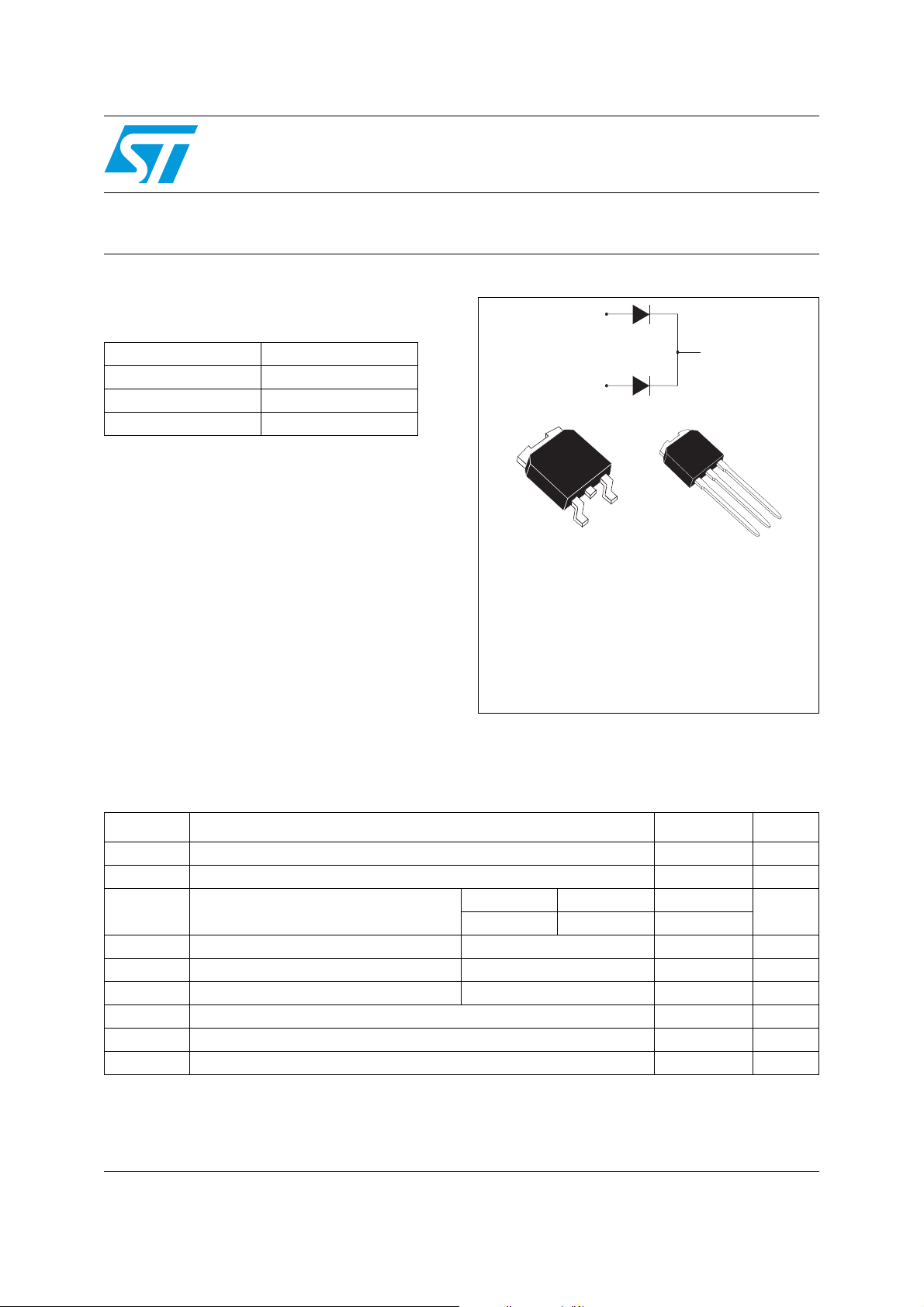
STPS15H100C
High voltage power Schottky rectifier
Main product characteristics
I
F(AV)
V
RRM
(max) 175° C
T
j
(max) 0.67 V
V
F
2 x 7.5 A
100 V
K
A1
K
A2
K
Features and Benefits
■ Negligible switching losses
■ Low leakage current
■ Good trade off between leakage current and
forward voltage drop
■ Low thermal resistance
■ Avalanche capability specified
STPS15H100CB
DPAK
A2
A1
STPS15H100CH
IPAK
Description
Dual center tab Schottky rectifier suited for
switched mode power supply and high frequency
DC to DC converters.
Packaged in DPAK and IPAK, this device is
intended for use in high frequency inverters.
Table 1. Absolute Ratings (limiting values, per diode)
Symbol Parameter Value Unit
A1
A2
K
V
RRM
I
F(RMS)
I
F(AV)
I
FSM
I
RRM
P
ARM
T
stg
T
Repetitive peak reverse voltage 100 V
RMS forward current 10 A
T
= 135° C Per diode 7.5
Average forward current
c
δ = 0.5 Per device 15
Surge non repetitive forward current tp = 10 ms sinusoidal 75 A
Peak repetitive reverse current tp = 2 µs square F= 1 kHz 1 A
Repetitive peak avalanche power tp = 1 µs Tj = 25° C 6600 W
Storage temperature range -65 to + 175 °C
Maximum operating junction temperature
j
(1)
175 °C
A
dV/dt Critical rate of rise of reverse voltage 10000 V/µs
dPtot
---------------
1. condition to avoid thermal runaway for a diode on its own heatsink
dTj
1
------------------ --------
<
Rth j a–()
June 2006 Rev 4 1/8
www.st.com
8
Characteristics STPS15H100C
1 Characteristics
Table 2. Thermal resistance
Symbol Parameter Value Unit
R
R
Junction to case
th(j-c)
Coupling 0.7
th(c)
°C/WTo ta l 2 .4
When the diodes 1 and 2 are used simultaneously :
Per diode 4
∆ T
(diode 1) = P(diode1) x R
j
Table 3. Static electrical characteristics (per diode)
(Per diode) + P(diode 2) x R
th(j-c)
th(c)
Symbol Parameter Test Conditions Min. Typ. Max. Unit
T
= 25° C
(1)
I
Reverse leakage current
R
j
T
= 125° C 1.3 4 mA
j
= V
V
R
RRM
3µA
Tj = 25° C IF = 7.5 A 0.8
Tj = 125° C IF = 7.5 A 0.62 0.67
T
= 25° C IF = 12 A 0.85
V
(1.) Forward voltage drop
F
j
T
= 125° C IF = 12 A 0.68 0.73
j
Tj = 25° C IF = 15 A 0.89
T
= 125° C IF = 15 A 0.71 0.76
j
1. Pulse test: tp = 380 µs, δ < 2%
To evaluate the conduction losses use the following equation:
P = 0.58 x I
F(AV)
+ 0.012 I
F2(RMS)
V
2/8
STPS15H100C Characteristics
9
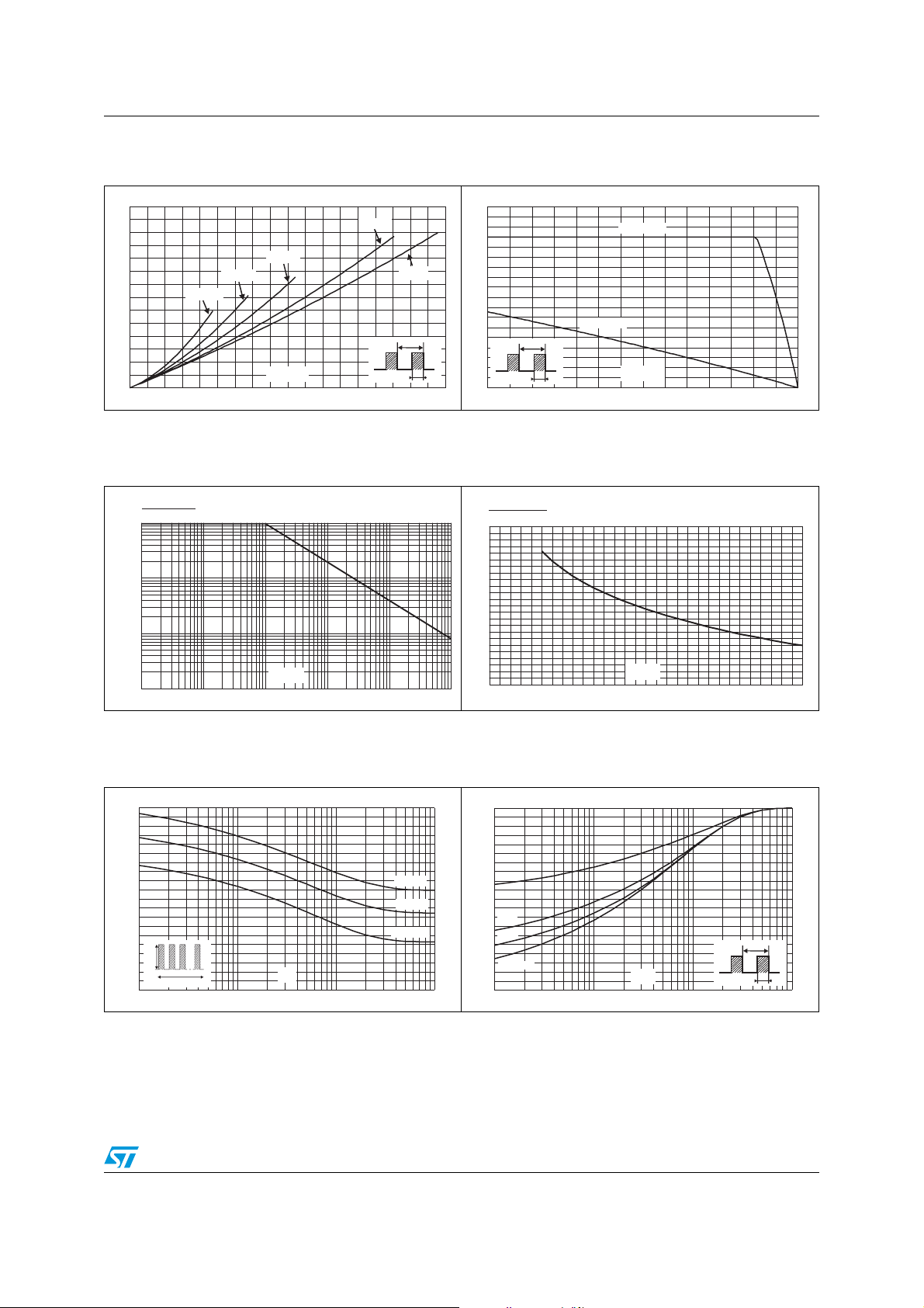
0
Figure 1. Conduction losses versus average
current
PF(av)(W)
7
6
5
4
3
2
1
0
012345678
δ = 0.05
δ = 0.2
δ = 0.1
IF(av)(A)
δ = 0.5
δ
=tp/T
δ = 1
T
tp
Figure 3. Normalized avalanche power
derating versus pulse duration
P(t)
ARM p
P (1µs)
ARM
1
0.1
0.01
t (µs)
0.001
0.10.01 1
p
10 100 1000
Figure 5. Non repetitive surge peak forward
current versus overload duration
(maximum values)
IM(A)
100
90
80
70
60
50
40
30
20
IM
10
0
1.E-03 1.E-02 1.E-01 1.E+0
δ=0.5
t
t(s)
Tc=25°C
Tc=75°C
Tc=125°C
Figure 2. Average forward current versus
ambient temperature (δ = 0.5)
IF(av)(A)
9
8
7
6
5
4
3
2
1
0
T
tp
=tp/T
δ
0 25 50 75 100 125 150 175
Rth(j-a)=Rth(j-c)
Rth(j-a)=70°C/W
Tamb(°C)
Figure 4. Normalized avalanche power
derating versus junction
temperature
P(t)
ARM p
P (25°C)
ARM
1.2
1
0.8
0.6
0.4
0.2
T (°C)
0
j
0 25 50 75 100 125 150
Figure 6. Relative variation of thermal
impedance junction to case versus
pulse duration
Zth(j-c)/Rth(j-c)
1.0
0.9
0.8
0.7
δ = 0.5
0.6
0.5
0.4
δ = 0.2
δ = 0.1
0.3
0.2
Single pulse
0.1
0.0
1.E-03 1.E-02 1.E-01 1.E+00
tp(s)
δ
=tp/T
T
tp
3/8
Characteristics STPS15H100C
0
6
Figure 7. Reverse leakage current versus
reverse voltage applied (typical
values)
IR(mA)
1.E+01
1.E+00
1.E-01
1.E-02
1.E-03
1.E-04
0 102030405060 70809010
Tj=150°C
Tj=125°C
Tj=100°C
Tj=75°C
Tj=50°C
Tj=25°C
VR(V)
Figure 9. Forward voltage drop versus
forward current
IFM(A)
100
Tj=125°C
Tj=125°C
(Maximum values)
(Maximum values)
Tj=125°C
Tj=125°C
(Typical values)
10
1
0.0 0.2 0.4 0.6 0.8 1.0 1.2 1.4 1.
(Typical values)
VFM(V)
Tj=25°C
(Maximum values)
Figure 8. Junction capacitance versus
reverse voltage applied (typical
values)
C(nF)
1.0
0.1
F=1MHz
Vosc=30mV
Tj=25°C
VR(V)
0.0
1 10 100
Figure 10. Thermal resistance junction to
ambient versus copper surface
under tab (epoxy printed board
FR4, Cu: 35µm)
Rth(j-a)(°C/W)
100
90
80
70
60
50
40
30
20
10
0
02468101214161820
S(cm²)
4/8

STPS15H100C Package Information
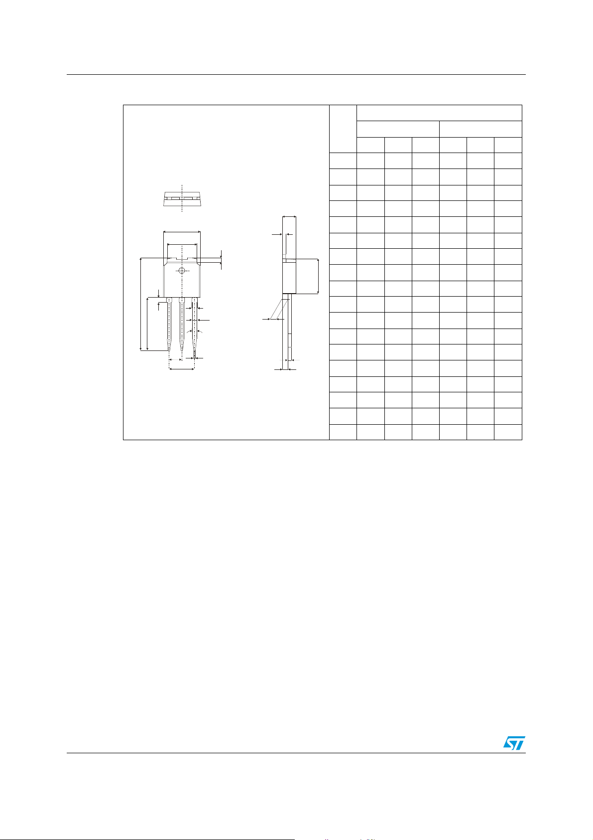
2 Package Information
Epoxy meets UL94,V0
Table 4. DPAK Package mechanical data
Dimensions
Ref
A 2.20 2.40 0.086 0.094
A1 0.90 1.10 0.035 0.043
A2 0.03 0.23 0.001 0.009
B 0.64 0.90 0.025 0.035
B2 5.20 5.40 0.204 0.212
C 0.45 0.60 0.017 0.023
C2 0.48 0.60 0.018 0.023
D 6.00 6.20 0.236 0.244
E 6.40 6.60 0.251 0.259
G 4.40 4.60 0.173 0.181
H 9.35 10.10 0.368 0.397
L2 0.80 typ. 0.031 typ.
L4 0.60 1.00 0.023 0.039
V2 0° 8° 0° 8°
Figure 11. DPAK Footprint (dimensions in mm)
Millimeters Inches
Min. Max. Min. Max.
6.7
6.7
3
3
1.61.6
2.32.3
5/8
Package Information STPS15H100C
Table 5. IPAK Package mechanical data
Dimensions
Ref.
A 2.20 2.40 0.086 0.094
A1 0.90 1.10 0.035 0.043
A3 0.70 1.30 0.027 0.051
A
E
B2
L2
C2
B 0.64 0.90 0.025 0.035
B2 5.20 5.40 0.204 0.212
B3 0.95 0.037
B5 0.30 0.035
C 0.45 0.60 0.017 0.023
D
C2 0.48 0.60 0.019 0.023
H
L1
L
B3
B
V1
A1
D 6 6.20 0.236 0.244
E 6.40 6.60 0.252 0.260
e 2.28 0.090
B5
e
G
C
A3
G 4.40 4.60 0.173 0.181
H 16.10 0.634
L 9 9.40 0.354 0.370
L1 0.8 1.20 0.031 0.047
L2 0.80 1 0.031 0.039
V1 10° 10°
Millimeters Inches
Min. Typ. Max. Min. Typ. Max.
6/8
STPS15H100C Ordering Information
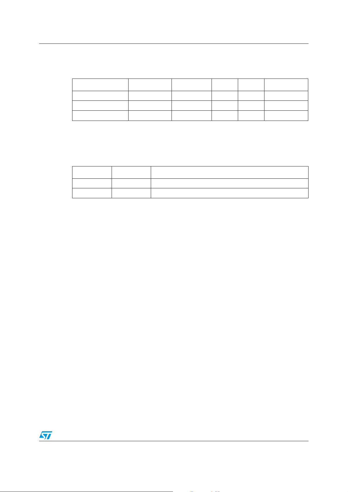
3 Ordering Information
Ordering type Marking Package Weight Base qty Delivery mode
STPS15H100CB S15H100 DPAK 0.30 g 75 Tube
STPS15H100CB-TR S15H100 DPAK 0.30 g 2500 Tape andreel
STPS15H100CH S15H100CH IPAK 0.35 g 75 Tube
4 Revision History
Date Revision Changes
Mar-2004 3 Last issue
08-Jun-2006 4 Reformatted to current standard. Added IPAK.
7/8

STPS15H100C
Please Read Carefully:
Information in this document is provided solely in connection with ST products. STMicroelectronics NV and its subsidiaries (“ST”) reserve the
right to make changes, corrections, modifications or improvements, to this document, and the products and services described herein at any
time, without notice.
All ST products are sold pursuant to ST’s terms and conditions of sale.
Purchasers are solely responsible for the choice, selection and use of the ST products and services described herein, and ST assumes no
liability whatsoever relating to the choice, selection or use of the ST products and services described herein.
No license, express or implied, by estoppel or otherwise, to any intellectual property rights is granted under this document. If any part of this
document refers to any third party products or services it shall not be deemed a license grant by ST for the use of such third party products
or services, or any intellectual property contained therein or considered as a warranty covering the use in any manner whatsoever of such
third party products or services or any intellectual property contained therein.
UNLESS OTHERWISE SET FORTH IN ST’S TERMS AND CONDITIONS OF SALE ST DISCLAIMS ANY EXPRESS OR IMPLIED
WARRANTY WITH RESPECT TO THE USE AND/OR SALE OF ST PRODUCTS INCLUDING WITHOUT LIMITATION IMPLIED
WARRANTIES OF MERCHANTABILITY, FITNESS FOR A PARTICULAR PURPOSE (AND THEIR EQUIVALENTS UNDER THE LAWS
OF ANY JURISDICTION), OR INFRINGEMENT OF ANY PATENT, COPYRIGHT OR OTHER INTELLECTUAL PROPERTY RIGHT.
UNLESS EXPRESSLY APPROVED IN WRITING BY AN AUTHORIZE REPRESENTATIVE OF ST, ST PRODUCTS ARE NOT DESIGNED,
AUTHORIZED OR WARRANTED FOR USE IN MILITARY, AIR CRAFT, SPACE, LIFE SAVING, OR LIFE SUSTAINING APPLICATIONS,
NOR IN PRODUCTS OR SYSTEMS, WHERE FAILURE OR MALFUNCTION MAY RESULT IN PERSONAL INJURY, DEATH, OR
SEVERE PROPERTY OR ENVIRONMENTAL DAMAGE.
Resale of ST products with provisions different from the statements and/or technical features set forth in this document shall immediately void
any warranty granted by ST for the ST product or service described herein and shall not create or extend in any manner whatsoever, any
liability of ST.
ST and the ST logo are trademarks or registered trademarks of ST in various countries.
Information in this document supersedes and replaces all information previously supplied.
The ST logo is a registered trademark of STMicroelectronics. All other names are the property of their respective owners.
© 2006 STMicroelectronics - All rights reserved
STMicroelectronics group of companies
Australia - Belgium - Brazil - Canada - China - Czech Republic - Finland - France - Germany - Hong Kong - India - Israel - Italy - Japan -
Malaysia - Malta - Morocco - Singapore - Spain - Sweden - Switzerland - United Kingdom - United States of America
www.st.com
8/8
 Loading...