


®
Table 1: Main Product Characteristics
I
F(AV)
V
RRM
T
(max) 150°C
j
(max) 0.5 V
V
F
1 A
40 V
STPS140
POWER SCHOTTKY RECTIFIER
FEATURES AND BENEFITS
■ Very small conduction losses
■ Negligible switching losses
■ Low forward voltage drop
■ Surface mount miniature packages
■ Avalanche capability specified
(JEDEC DO-214AC)
SMA
STPS140A
SMB
(JEDEC DO-214AA)
STPS140U
DESCRIPTION
Single chip Schottky rectifiers suited to Switched
Mode Power Supplies and high frequency DC to
DC converters.
Packaged in SMA and SMB, this device is
Table 2: Order Codes
Part Number Marking
STPS140A S140
STPS140U G14
especially intended for surface mounting and used
in low voltage, high frequency inverters, free
wheeling and polarity protection applications.
Table 3: Absolute Ratings (limiting values)
Symbol Parameter Value Unit
V
RRM
I
F(RMS)
I
F(AV)
I
FSM
I
RRM
I
RSM
P
ARM
T
T
Repetitive peak reverse voltage 40 V
RMS forward voltage 7 A
Average forward current
SMA T
SMB T
= 130°C δ = 0.5
L
= 135°C δ = 0.5
L
Surge non repetitive forward current tp = 10ms sinusoidal 60 A
Repetitive peak reverse current tp = 2µs F = 1kHz square 1 A
Non repetitive peak reverse current tp = 100µs square 1 A
Repetitive peak avalanche power tp = 1µs Tj = 25°C 900 W
Storage temperature range -65 to + 150 °C
stg
Maximum operating junction temperature * 150 °C
j
1A
dV/dt Critical rate of rise of reverse voltage 10000 V/µs
dPtot
* : thermal runaway condition for a diode on its own heatsink
------------- --
dTj
1
--------------- ----------->
Rth j a
–()
August 2004
REV. 8
1/7
STPS140
Table 4: Thermal Resistance
Symbol Parameter Value Unit
R
th(j-l)
Junction to lead
Table 5: Static Electrical Characteristics
Symbol Parameter Tests conditions Min. Typ Max. Unit
= 25°C
T
I
*
R
V
F
Reverse leakage current
**
Forward voltage drop
j
= 100°C
T
j
T
= 25°C
j
= 125°C
T
j
T
= 25°C
j
T
= 125°C
j
Pulse test: * tp = 5 ms, δ < 2%
** tp = 380 µs,
δ < 2%
To evaluate the conduction losses use the following equation: P = 0.4 x I
V
R
I
F
I
F
= V
= 1A
= 2A
F(AV)
SMA 30
SMB 25
RRM
0.25 2
0.43 0.45
0.53 0.6
+ 0.10 I
F2(RMS)
°C/W
12
0.55
0.65
µA
mA
V
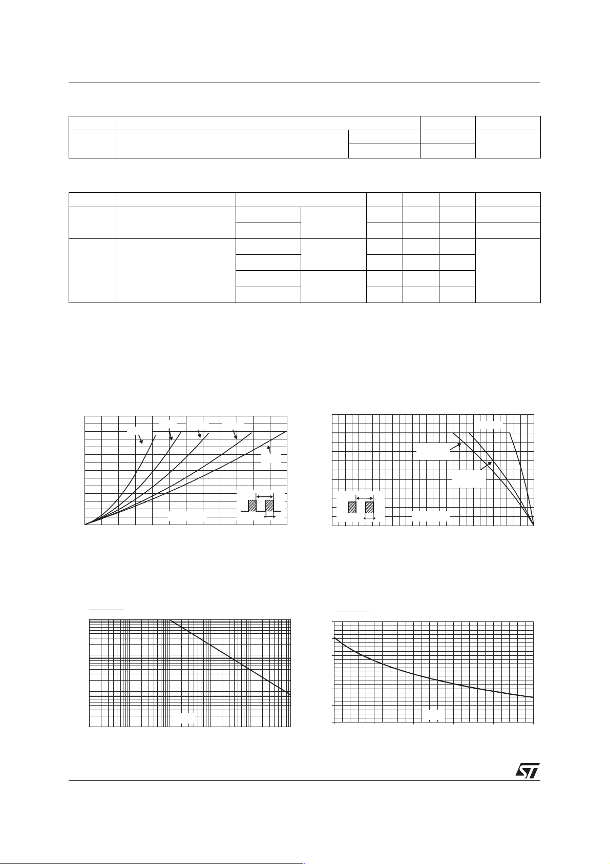
Figure 1: Average forward power dissipation
versus average forward current
P (W)
F(AV)
0.7
0.6
0.5
0.4
0.3
0.2
0.1
0.0
0.0 0.2 0.4 0.6 0.8 1.0 1.2
δ = 0.05
δ = 0.1
δ = 0.2
I (A)
F(AV)
δ = 0.5
δ
=tp/T
δ = 1
T
tp
Figure 3: Normalized avalanche power
derating versus pulse duration
P(t)
ARM p
P (1µs)
ARM
1
0.1
0.01
t (µs)
0.001
0.10.01 1
p
10 100 1000
Figure 2: Average forward current versus
ambient temperature (δ = 0.5)
I (A)
F(AV)
1.2
1.0
SMA
R =100°C/W
0.8
0.6
0.4
0.2
0.0
0 25 50 75 100 125 150
δ
=tp/T
T
tp
th(j-a)
S =1.5cm
(CU)
T (°C)
amb
2
SMB
R =80°C/W
th(j-a)
S =1.5cm
(CU)
R=R
th(j-a) th(j-I)
2
Figure 4: Normalized avalanche power
derating versus junction temperature
P(t)
ARM p
P (25°C)
ARM
1.2
1
0.8
0.6
0.4
0.2
0
25 50 75 100 125 150
T (°C)
j
2/7
STPS140
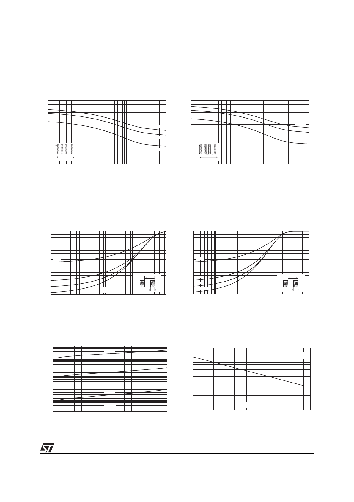
Figure 5: Non repetitive surge peak forward
current versus overload duration (maximum
values) (SMA)
I (A)
M
8
7
6
5
4
3
2
IM
1
0
1E-3 1E-2 1E-1 1E+0
δ=0.5
t
t(s)
T =25°C
a
T =50°C
a
T =100°C
a
Figure 7: Relative variation of thermal
impedance junction to ambient versus pulse
duration (epoxy printed circuit board,
e(Cu)=35µm, recommended pad layout) (SMA)
Z/R
th(j-c) th(j-c)
1.0
0.9
0.8
0.7
0.6
δ = 0.5
0.5
0.4
0.3
δ = 0.2
0.2
δ = 0.1
0.1
Single pulse
0.0
1E-2 1E-1 1E+0 1E+1 1E+2
t (s)
p
δ
=tp/T
T
tp
Figure 6: Non repetitive surge peak forward
current versus overload duration (maximum
values) (SMB)
I (A)
M
8
7
6
T =25°C
5
4
3
2
I
M
1
0
1E-3 1E-2 1E-1 1E+0
t
δ
=0.5
t(s)
a
T =50°C
a
T =100°C
a
Figure 8: Relative variation of thermal
impedance junction to ambient versus pulse
duration (epoxy printed circuit board,
e(Cu)=35µm, recommended pad layout) (SMB)
Z/R
th(j-c) th(j-c)
1.0
0.9
0.8
0.7
0.6
δ
= 0.5
0.5
0.4
0.3
δ
= 0.2
0.2
δ
= 0.1
0.1
Single pulse
0.0
1E-2 1E-1
1E+0
t (s)
p
1E+1 1E+2
δ
=tp/T
T
tp
1E+3
Figure 9: Reverse leakage current versus
reverse voltage applied (typical values)
I (µA)
R
1E+3
1E+2
1E+1
1E+0
1E-1
1E-2
0 5 10 15 20 25 30 35 40
T =125°C
j
T =75°C
j
T =25°C
j
V (V)
R
Figure 10: Junction capacitance versus
reverse voltage applied (typical values)
C(pF)
200
100
50
20
V (V)
10
12 51020 50
R
F=1MHz
T =25°C
j
3/7
 Loading...