


Power Schottky rectifier in flat package
Features
■ Very low profile package: 0.85 mm
■ Backward compatible with standard STmite
footprint
■ Very small conduction losses
■ Negligible switching losses
■ Extremely fast switching
■ Low forward voltage drop for higher efficiency
and extended battery life
■ Low thermal resistance
■ Avalanche capability specified
■ Hologen free molding compound
Description
STPS120MF
K
STmite flat
(DO222-AA)
Table 1. Device summary
I
F(AV)
V
RRM
(max) 150 °C
T
j
V
(max) 0.41 V
F
A
1 A
20 V
Single Schottky rectifier suited for switch mode
power supplies and high frequency dc to dc
converters.
Packaged in STmite flat, this device is intended
for use in low voltage, high frequency inverters,
free wheeling and polarity protection applications.
Due to the very small size of the package this
device fits battery powered equipment (cellular,
notebook, PDA’s, printers) as well as chargers
and PCMCIA cards.
May 2008 Rev 1 1/7
www.st.com

Characteristics STPS120MF
1 Characteristics
Table 2. Absolute ratings (limiting values)
Symbol Parameter Value Unit
V
RRM
I
F(RMS)
I
F(AV)
I
FSM
P
ARM
T
stg
T
Repetitive peak reverse voltage 20 V
Forward current rms 2 A
Average forward current Tc = 140 °C δ = 0.5 1 A
Surge non repetitive forward current tp = 10 ms sinusoidal 50 A
Repetitive peak avalanche power tp = 1 µs Tj = 25 °C 1400 W
Storage temperature range -65 to + 150 °C
Maximum operating junction temperature
j
(1)
150 °C
dV/dt Critical rate of rise of reverse voltage (rated VR, Tj = 25 °C) 10000 V/µs
dPtot
---------------
1. condition to avoid thermal runaway for a diode on its own heatsink
dTj
Table 3. Thermal resistance
1
--------------------------
<
Rth j a–()
Symbol Parameter Value Unit
R
th(j-c)
R
th(j-a)
1. Mounted with minimum recommended pad size, PC board FR4
Table 4. Static electrical characteristics
Junction to case 20 °C/W
(1)
Junction to ambient 250 °C/W
Symbol Parameter Test conditions Min. Typ. Max. Unit
(1)
I
V
1. Pulse test: tp = 380 µs, δ < 2%
Reverse leakage current
R
(1)
Forward voltage drop
F
Tj = 25° C
VR = V
V
R
V
R
I
= 1 A
F
= 2 A
I
F
RRM
= 10 V
= 5 V
= 100° C 275 850
T
j
= 25° C
T
j
T
= 100° C 145 450
j
= 25° C
T
j
T
= 100° C 105 300
j
= 25° C
T
j
T
= 100° C 0.36 0.41
j
= 25° C
T
j
T
= 100° C 0.42 0.48
j
1.3 3.9
0.6 2.0
0.4 10.
0.44 0.49
0.48 0.54
To evaluate the conduction losses use the following equation:
P = 0.34 x I
F(AV)
+ 0.07 I
F2(RMS)
µA
V
2/7
STPS120MF Characteristics
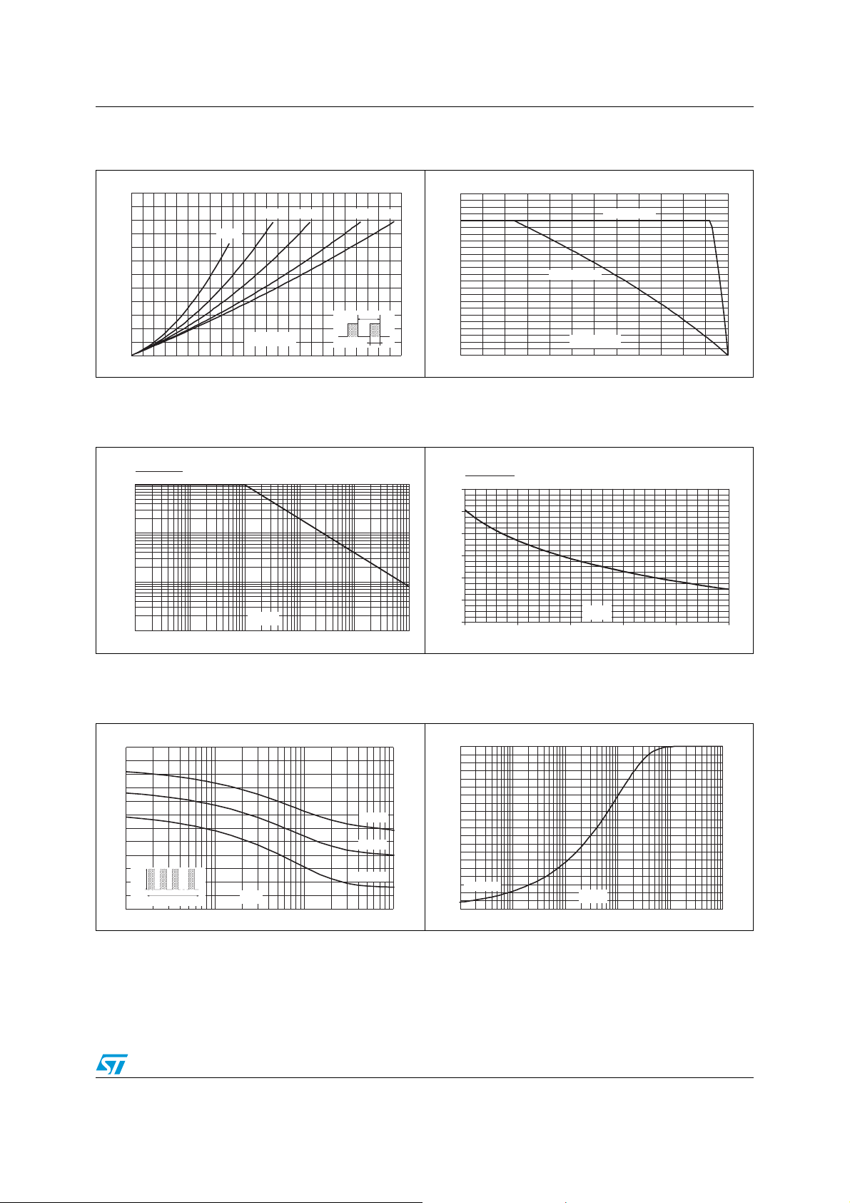
Figure 1. Conduction losses versus average
current
P (W)
F(AV)
0.6
δ=0.1
0.5
0.4
0.3
0.2
0.1
0.0
0.0 0.1 0.2 0.3 0.4 0.5 0.6 0.7 0.8 0.9 1.0 1.1 1.2
δ=0.05
I (A)
F(AV)
δ=0.2
δ
=tp/T
δ=0.5
δ=1
T
tp
Figure 3. Normalized avalanche power
derating versus pulse duration
P(tp)
ARM
P (1 µs)
ARM
1
0.1
0.01
t (µs)
0.001
0.10.01 1
p
10 100 1000
Figure 2. Average forward current versus
ambient temperature (δ = 0.5)
I (A)
F(AV)
1.2
1.1
1.0
0.9
0.8
0.7
0.6
0.5
0.4
0.3
0.2
0.1
0.0
0 25 50 75 100 125 150
R
th(j-a)
=250°C/W
T (°C)
amb
R
th(j-a)=Rth(j-c)
Figure 4. Normalized avalanche power
derating versus junction
temperature
P(Tj)
ARM
P (25 °C)
ARM
1.2
1
0.8
0.6
0.4
0.2
0
25 50 75 100 125 150
T (°C)
j
Figure 5. Non repetitive surge peak forward
current versus overload duration
(maximum values)
I (A)
M
6
5
4
3
2
I
M
1
0
1.E-03 1.E-02 1.E-01 1.E+00
t
=0.5
δ
t(s)
Ta=25°C
Ta=75°C
Ta=125°C
Figure 6. Relative variation of thermal
impedance junction to ambient
versus pulse duration
Z/R
th(j-a) th(j-a)
1.0
0.9
0.8
0.7
0.6
0.5
0.4
0.3
0.2
Single pulse
0.1
0.0
1.E-02 1.E-01 1.E+00 1.E+01 1.E+02 1.E+03
3/7
t (s)
p
 Loading...