

ST STPS1045B-Y User Manual

Features
STPS1045B-Y
Automotive power Schottky rectifier
■ Negligible switching losses
■ Low forward voltage drop
■ Low capacitance
■ High reverse avalanche surge capability
■ Avalanche specification
■ AEC-Q101 qualified
Description
High voltage Schottky rectifier suited for switch
mode power supplies and other power converters.
Packaged in DPAK, this device is intended for use
in high frequency circuits where low switching
losses are required.
K
K
A
A
DPAK
STPS1045BY
j
Table 1. Device summary
I
F(AV)
V
RRM
T
j
V
(max) 0.57 V
F
10 A
45 V
175 °C
May 2011 Doc ID 17265 Rev 1 1/7
www.st.com
7

Characteristics STPS1045B-Y
1 Characteristics
Table 2. Absolute maximum ratings
Symbol Parameter Value Unit
V
I
F(RMS)
I
F(AV)
I
I
P
T
RRM
FSM
RRM
ARM
T
Repetitive peak reverse voltage 45 V
/pin Forward rms current 7 A
Average forward current Tc = 150 °C δ = 0.5 10 A
Surge non repetitive forward current tp = 10 ms sinusoidal 75 A
Repetitive peak reverse current tp = 2 µs, F= 1 kHz 1 A
Repetitive peak avalanche power tp = 1 µs, T
Storage temperature range -65 to +175 °C
stg
Operating junction temperature range
j
(1)
25 °C 4000 W
j =
-40 to +175 °C
dV/dt Critical rate of rise of reverse voltage 10000 V/µs
dPtot
---------------
1. condition to avoid thermal runaway for a diode on its own heatsink
dTj
Table 3. Thermal parameters
1
------------------------- -
<
Rth j a–()
Symbol Parameter Value Unit
R
th(j-c)
Table 4. Static electrical characteristics
Junction to case 3 °C/W
Symbol Parameter Test conditions Min. Typ. Max. Unit
Reverse leakage
(1)
I
R
current
(2)
V
1. Pulse test: tp = 5 ms, δ < 2%
2. Pulse test: tp = 380 µs, δ < 2%
Forward voltage drop
F
= 25 °C
T
j
T
= 125 °C - 7 15 mA
j
= 25 °C
T
j
T
= 125 °C - 0.50 0.57
j
T
= 25 °C
j
= 125 °C - 0.65 0.72
T
j
= V
V
R
= 10 A
I
F
= 20 A
I
F
RRM
- - 100 μA
- - 0.63
- - 0.84
V
To evaluate the conduction losses use the following equation:
P = 0.42 x I
2/7 Doc ID 17265 Rev 1
F(AV)
+ 0.015 I
F2(RMS)
STPS1045B-Y Characteristics
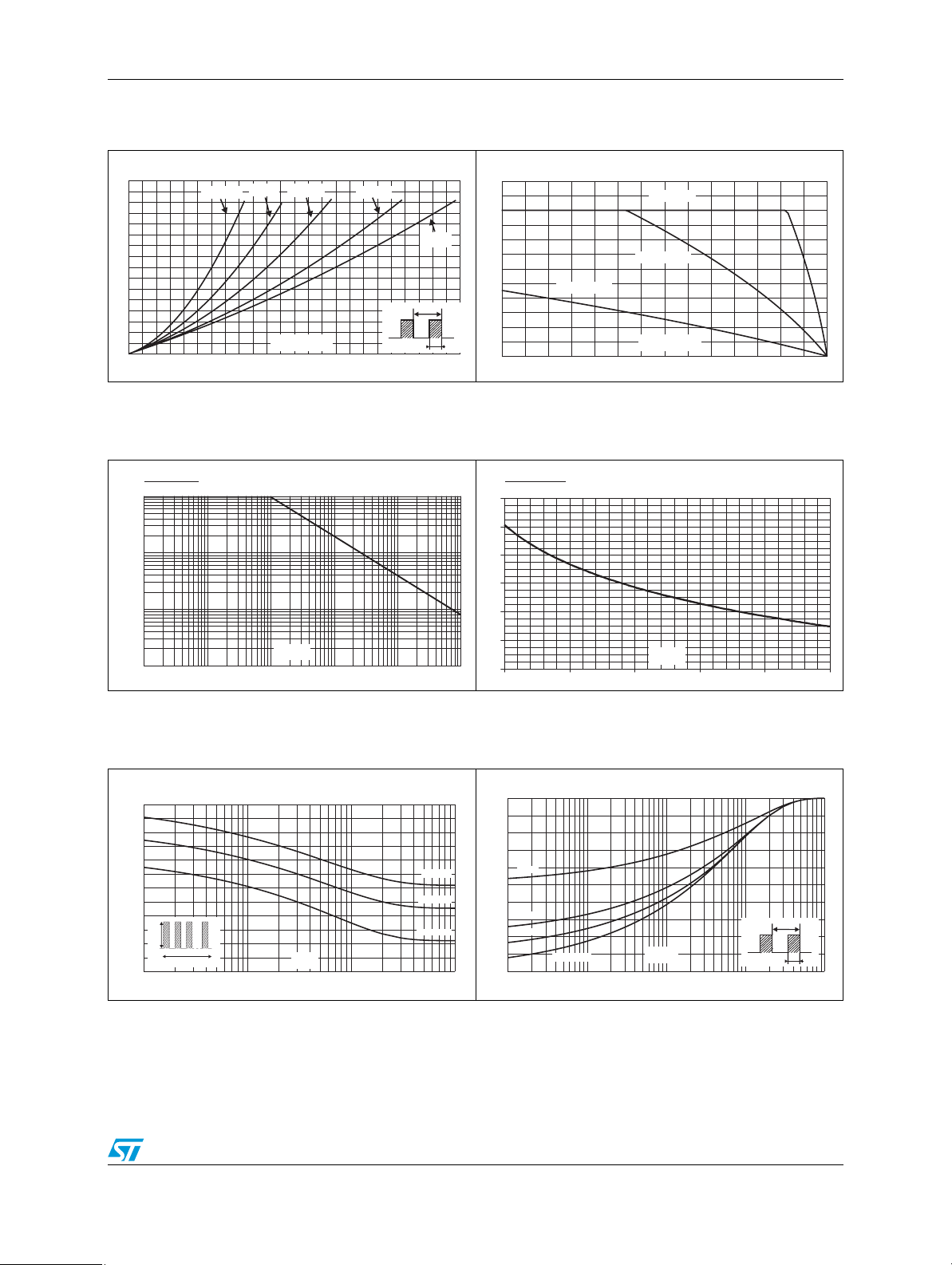
Figure 1. Average forward power dissipation
versus average forward current
P(W)
F(AV)
8
7
6
5
4
3
2
1
0
0123456789101112
δ = 0.05
δ = 0.1
δ = 0.2
I (A)
F(AV)
δ = 0.5
δ
=tp/T
δ = 1
T
tp
Figure 3. Normalized avalanche power
derating versus pulse duration
P(t)
ARM p
P (1µs)
ARM
1
0.1
Figure 2. Average forward current versus
ambient temperature (
I (A)
F(AV)
12
10
8
6
R =70°C/W
4
2
0
0 25 50 75 100 125 150 175
th(j-a)
R=R
th(j-a) th(j-c)
R =15°C/W
th(j-a)
T (°C)
amb
δ = 0.5)
Figure 4. Normalized avalanche power
derating versus junction
temperature
P(T)
ARM
P (25 °C)
1.2
1
0.8
j
ARM
0.01
t (µs)
0.001
0.10.01 1
p
10 100 1000
Figure 5. Non repetitive surge peak forward
current versus overload duration
(maximum values)
I (A)
M
120
100
80
60
40
IM
20
0
1E-3 1E-2 1E-1 1E+0
δ=0.5
t
t(s)
T =50°C
C
T =100°C
C
T =150°C
C
0.6
0.4
0.2
0
25 50 75 100 125 150
T (°C)
j
Figure 6. Relative variation of thermal
impedance junction to case versus
pulse duration
Z/R
th(j-c) th(j-c)
1.0
0.8
0.6
δ = 0.5
0.4
δ = 0.2
δ = 0.1
0.2
0.0
Single pulse
1E-4 1E-3 1E-2 1E-1 1E+0
t (s)
p
δ
T
=tp/T
tp
Doc ID 17265 Rev 1 3/7
 Loading...