


Features
STPMS1
Dual-channel 1-bit, 2 MHz, 1st order
sigma-delta modulator with embedded PGA
■ V
■ Two 1
■ Programmable chopper-stabilized low noise
supply range: 3.2 V - 5.5 V
CC
st
order sigma-delta modulators
and low offset amplifier
■ Supports 50-60 Hz AC watt meters
■ Internal low-drop regulator at 3 V (typ.)
■ Precision voltage reference: 1.23 V and 30
ppm/°C (typ.)
Applications
■ Power metering
■ Motor control
■ Industrial process control
■ Weight scale
■ Pressure transducers
Description
The STPMS1, also called a smart-sensor device,
is an ASSP designed for effective measurement
in power line systems utilizing the Rogowski coil,
current transformer, or shunt principle. It is used
in combination with the STPMC1 programmable
poly-phase energy calculator IC, as a building
block for single-phase or poly-phase energy
meters. The STPMS1 is a mixed signal IC
consisting of an analog and a digital section. The
analog section consists of a pre-amplifier and two
st
1
order ΣΔ modulator blocks, band-gap voltage
reference, a low-drop voltage regulator, and DC
buffers, while the digital section consists of a clock
generator and output multiplexer. This device is
designed for use in medium resolution
Table 1. Device summary
QFN16 (3 x 3 mm.)
measurement applications when single or double
inputs must be monitored at the same time.
Order code Package Packaging
STPMS1BPQR QFN16 (3 x 3 mm) 2500 parts per reel
October 2010 Doc ID 16524 Rev 2 1/23
www.st.com
23

Contents STPMS1
Contents
1 Schematic diagram . . . . . . . . . . . . . . . . . . . . . . . . . . . . . . . . . . . . . . . . . . 3
2 Pin configuration . . . . . . . . . . . . . . . . . . . . . . . . . . . . . . . . . . . . . . . . . . . . 4
3 Electrical characteristics . . . . . . . . . . . . . . . . . . . . . . . . . . . . . . . . . . . . . 5
4 General operating conditions . . . . . . . . . . . . . . . . . . . . . . . . . . . . . . . . . 6
5 Application . . . . . . . . . . . . . . . . . . . . . . . . . . . . . . . . . . . . . . . . . . . . . . . . . 9
6 Terminology . . . . . . . . . . . . . . . . . . . . . . . . . . . . . . . . . . . . . . . . . . . . . . . 12
6.1 Conventions . . . . . . . . . . . . . . . . . . . . . . . . . . . . . . . . . . . . . . . . . . . . . . . 12
6.2 Notation . . . . . . . . . . . . . . . . . . . . . . . . . . . . . . . . . . . . . . . . . . . . . . . . . . 12
7 Typical performance characteristics . . . . . . . . . . . . . . . . . . . . . . . . . . . 13
8 Theory of operation . . . . . . . . . . . . . . . . . . . . . . . . . . . . . . . . . . . . . . . . 15
8.1 General operation description . . . . . . . . . . . . . . . . . . . . . . . . . . . . . . . . . 15
8.2 Function description of the analog part . . . . . . . . . . . . . . . . . . . . . . . . . . 15
8.3 Functional description of the digital part . . . . . . . . . . . . . . . . . . . . . . . . . . 17
9 Package mechanical data . . . . . . . . . . . . . . . . . . . . . . . . . . . . . . . . . . . . 18
10 Revision history . . . . . . . . . . . . . . . . . . . . . . . . . . . . . . . . . . . . . . . . . . . 22
2/23 Doc ID 16524 Rev 2
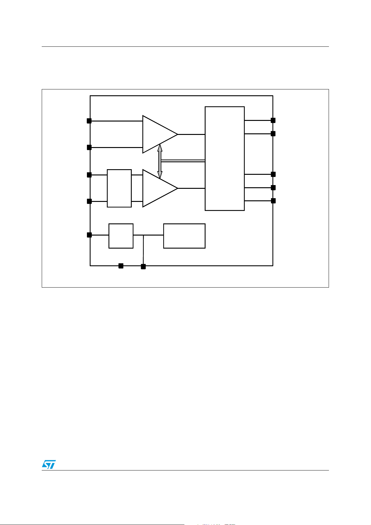
STPMS1 Schematic diagram
1 Schematic diagram
Figure 1. Block diagram
DAT
VIP
VIP
VIN
VIN
CIP
CIP
CIN
CIN
PGA
PGA
8x, 32x
8x, 32x
1stord
1stord
modulator
modulator
1stord
1stord
modulator
modulator
ΣΔ
ΣΔ
ΣΔ
ΣΔ
DIGITAL
DIGITAL
FRONT
FRONT
END
END
DAT
DATN
DATN
MS1
MS1
MS0
MS0
CLK
CLK
VCC
VCC
LDO
LDO
BIAS
BIAS
Ref
Ref
AM07830v1
AM07830v1
VDDGND
VDDGND
Doc ID 16524 Rev 2 3/23
Pin configuration STPMS1
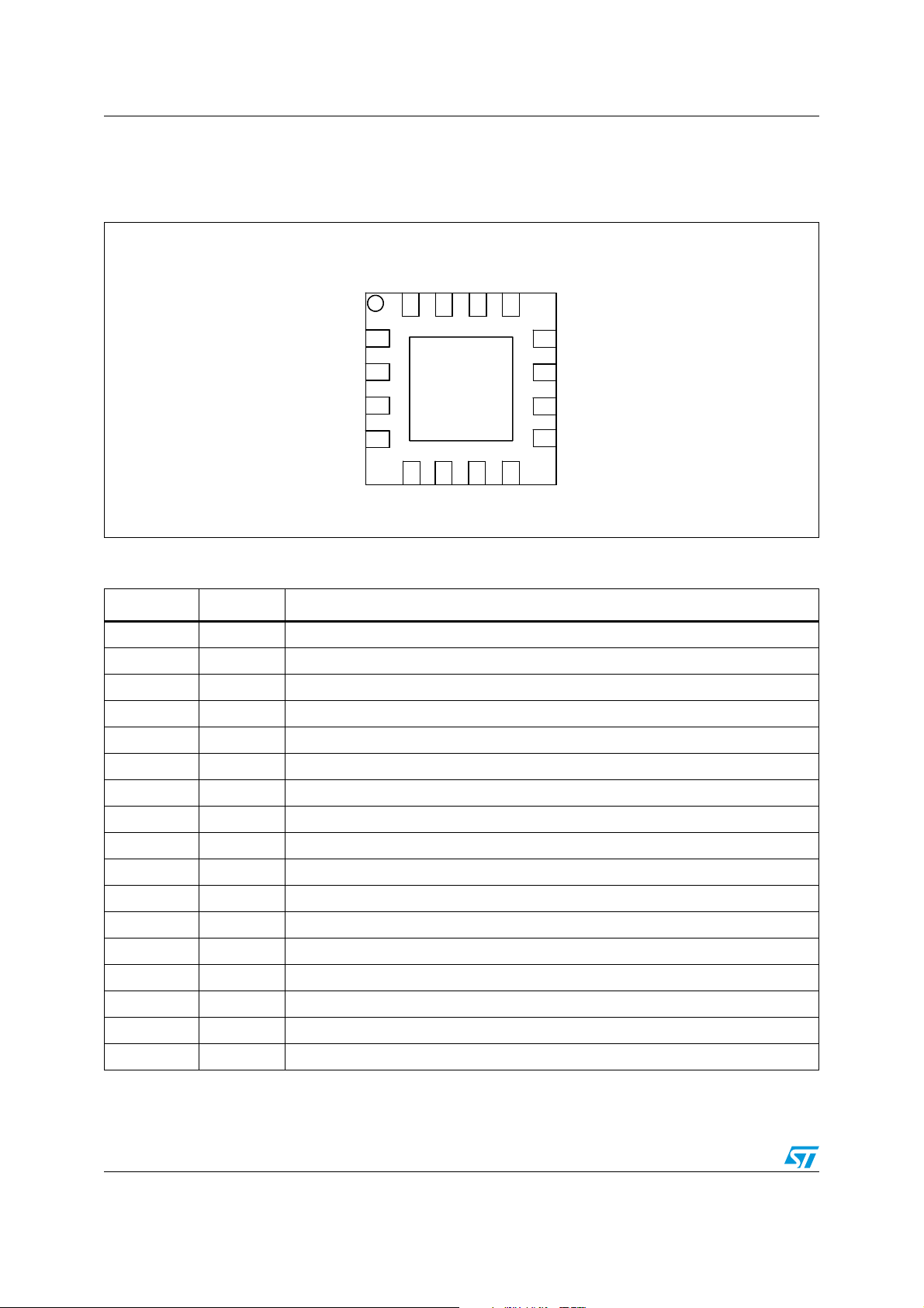
2 Pin configuration
Figure 2. Pin connection (top view)
DAT
VDD
VDD
GND
GND
VDDac
VDDac
GND
GND
DAT
VCC
VCC
1
1
GND
GND
CIP
CIP
CIN
CIN
DATN
DATN
VIP
VIP
CLK
CLK
VIN
VIN
MS1
MS1
MS0
MS0
VDDd
VDDd
VDDav
VDDav
AM07831v1
AM07831v1
Table 2. Pin description
Pin Symbol Description
1 VDD + 3.0 V output of LDO
2 GND Ground level for signals and pin protection
3 VDDac Current channel modulator supply input
4 GND Ground level for signals and pin protection
5 CIP Current channel +
6 CIN Current channel -
7 VIP Voltage channel +
8 VIN Voltage channel -
9 VDDav Voltage channel modulator supply input
10 VDDd Digital front-end supply input
11 MS0 Input for configurator 0
12 MS1 Input for configurator 1
13 CLK Input for external measurement clock
14 DAT Output of multiplexed ΣΔ signal
15 DATn Output of multiplexed ΣΔ signal negated
16 VCC Unregulated supply voltage
Exp PAD GND Ground level for signals and pin protection
4/23 Doc ID 16524 Rev 2
STPMS1 Electrical characteristics
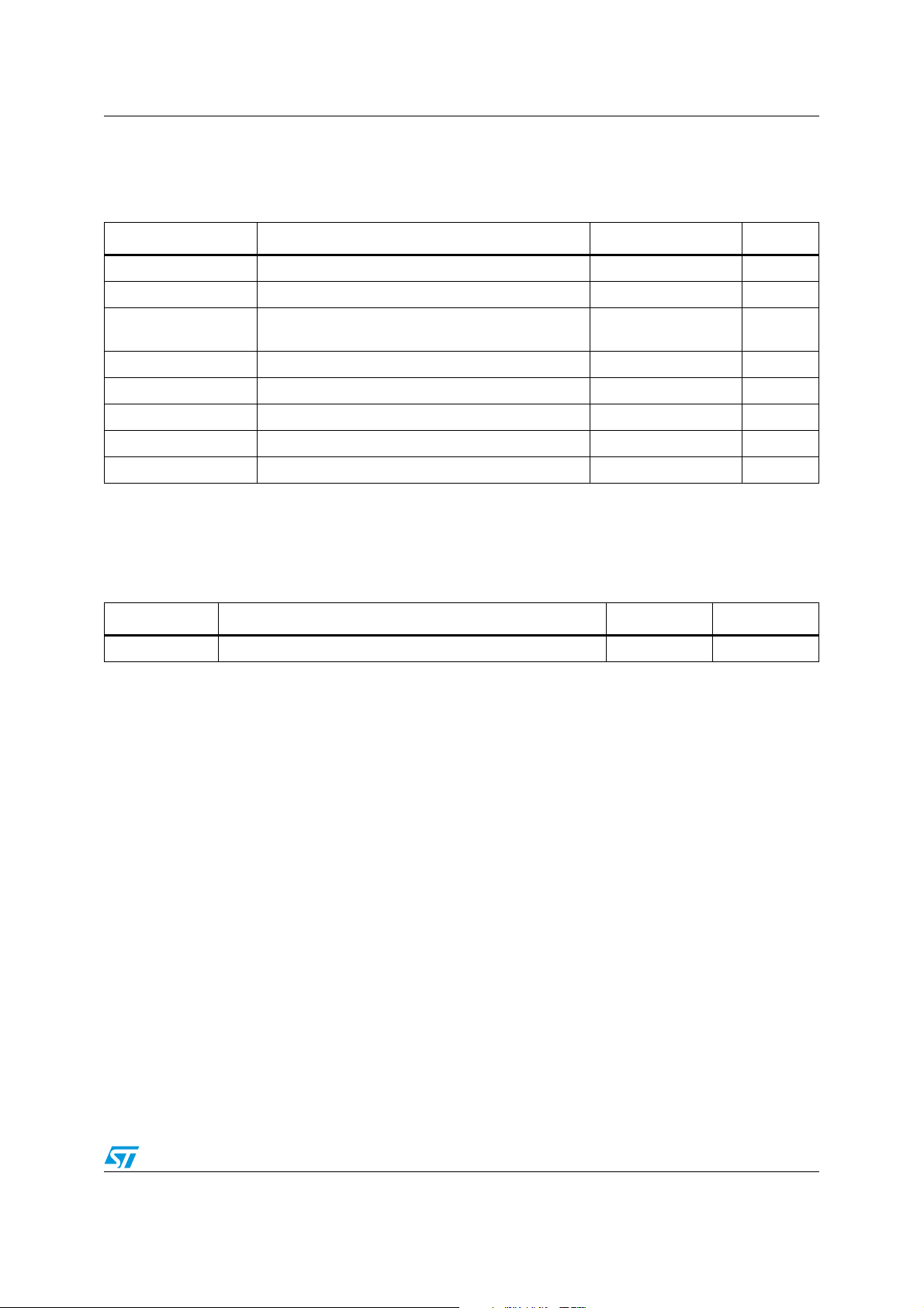
3 Electrical characteristics
Table 3. Absolute maximum ratings
Symbol Parameter Value Unit
VCC DC input voltage -0.3 to 6 V
I
PIN
V
ID
V
IA
ESD Human body model (all pins) ±3.5 kV
T
OP
T
J
T
STG
Note: Absolute maximum ratings are those values beyond which damage to the device may occur.
Functional operation under these conditions is not implied.
Current on any pin (sink/source) ±150 mA
Input voltage at digital pins (MS0, MS1, CLK, DAT,
DATN)
-0.3 to V
+0.3 V
CC
Input voltage at analog pins (VIP, VIN, CIP, CIN) -0.7 to 0.7 V
Operating ambient temperature -40 to 85 °C
Junction temperature -40 to 150 °C
Storage temperature range -55 to 150 °C
Table 4. Thermal data
Symbol Parameter Value Unit
R
thJA
1. This value refers to a single-layer PCB, JEDEC standard test board.
Thermal resistance junction-ambient 38.10
(1)
°C/W
Doc ID 16524 Rev 2 5/23
General operating conditions STPMS1
4 General operating conditions
VCC = 5 V, TA = 25 °C, 2.2 µF between VDD and GND, 100 nF between VCC and GND,
f
= 2.048 MHz unless otherwise specified.
CLK
Table 5. General operating conditions
Symbol Parameter Test conditions Min. Typ. Max. Unit
General section
V
I
V
V
I
LATCH
f
Operating supply voltage 3.165 5.5 V
CC
Quiescent current
CC
Power on reset on V
POR
Regulated supply voltage 1.049 MHz; VCC=3.2 V; CL=100 nF, no loads 2.85 3.00 3.15 V
DD
Current injection latch-up
immunity
Nominal frequencies 1.0 2.458 MHz
CLK
DC measurement accuracy
Resolution 11 16 bit
INL Integral non-linearity
DNL Differential linearity
Offset error
Gain error
1.049 MHz; V
=3.165 V; CL=100 nF, no
CC
loads
CC
Result referred to a 13-bit resolution of CIPCIN channel
Result referred to a 9-bit resolution of VIPVIN channel
Result referred to a 13-bit resolution of CIPCIN channel
Result referred to a 9-bit resolution of VIPVIN channel
Result referred to a 13-bit resolution of CIPCIN channel
Result referred to a 9-bit resolution of VIPVIN channel
Result referred to a 13-bit resolution of CIPCIN channel
Result referred to a 9-bit resolution of VIPVIN channel
2.5 mA
2.5 V
300 mA
0.35
LSB
0.5
0.2
LSB
0.4
0.15
LSB
0.05
0.05
LSB/
µV
0.001
NF Noise floor CIP-CIN channel, Gain 8x 115 dB
rms
rms
/50 Hz
/50 Hz
0.2 %
PSRR
Power supply DC
DC
rejection
Voltage signal: 200 mV
Current signal: 10 mV
f
= 2.048 MHz
CLK
=3.3 V±10 %, 5 V±10 %
V
CC
6/23 Doc ID 16524 Rev 2

STPMS1 General operating conditions
Table 5. General operating conditions (continued)
Symbol Parameter Test conditions Min. Typ. Max. Unit
AC measurement accuracy
SNR Signal to noise ratio
SINAD
Signal to noise ratio +
distortion
THD Total harmonic distortion
SFDR
PSRR
Spurious free dynamic
range
Power supply AC
AC
rejection
Analog inputs (CIP, CIN, VIP, VIN)
V
Maximum input signal
MAX
levels
CIP-CIN channel – Vin=±120 mV @ 55 Hz
Gain 8x
65 dB
VIP-VIN channel – Vin=±230 mV @ 55 Hz 50
CIP-CIN channel – Vin=±120 mV @ 55 Hz
Gain 8x
65
dB
VIP-VIN channel – Vin=±230 mV @ 55 Hz 50
CIP-CIN channel – Vin=±120 mV @ 55 Hz
Gain 8x
-80
dB
VIP-VIN channel – Vin=±230 mV @ 55 Hz -70
CIP-CIN channel – Vin=±120 mV @ 55 Hz
Gain 8x
80
dB
VIP-VIN channel – Vin=±230 mV @ 55 Hz 50
Voltage signal: 200 mV
Current signal: 10 mV
= 2.048 MHz
f
CLK
=3.3 V+0.2 V
V
CC
VCC=5.0 V+0.2 V
rms
rms
/50 Hz
rms
/50 Hz
rms
1 @100 Hz
1 @100 Hz
0.1 %
VIP-VIN channel -0.3 +0.3 V
CIP-CIN channel
Gain 8X
Gain 32X
-0.15
-0.035
+0.15
+0.035
V
f
V
Z
G
I
A/D sampling frequency f
SPL
Amplifier offset ±20 mV
off
VIP, VIN impedance Over the total operating voltage range 200 400 kΩ
Z
IP
CIP, CIN impedance Over the total operating voltage range 240 kΩ
IN
Current channel gain
ERR
error
Voltage channel leakage
ILV
current
Current channel leakage
I
ILI
current
V
CC
Input enabled -10 10
Digital I/O (CLK, DAT, DATn, MS0, MS1)
V
Input high voltage
IH
Input low voltage -0.3
V
IL
/2 Hz
CLK
±10 %
= 5.3 V, f
= 1.049 MHz -1 1
CLK
-1 1
0.75
V
CC
0.25V
Doc ID 16524 Rev 2 7/23
µA
5.3 V
CC
V
 Loading...