

ST STPM11, STPM12, STPM13, STPM14 User Manual

Single phase energy metering IC with pulsed output
Features
■ Ripple free active energy pulsed output
■ Direct stepper counter drivers
■ Shunt, current transformer, Rogowsky coil
sensors
■ Live and neutral monitoring (STPM13/14)
■ Easy and fast digital calibration at only one
load point
■ No-load, negative power and tamper indicators
■ Integrated linear VREGs
■ RC (STPM11/13) or crystal oscillator
(STPM12/14)
■ Support 50 ÷ 60 Hz - IEC62052-11, IEC62053-
2X specification
■ Less than 0.1% error
Description
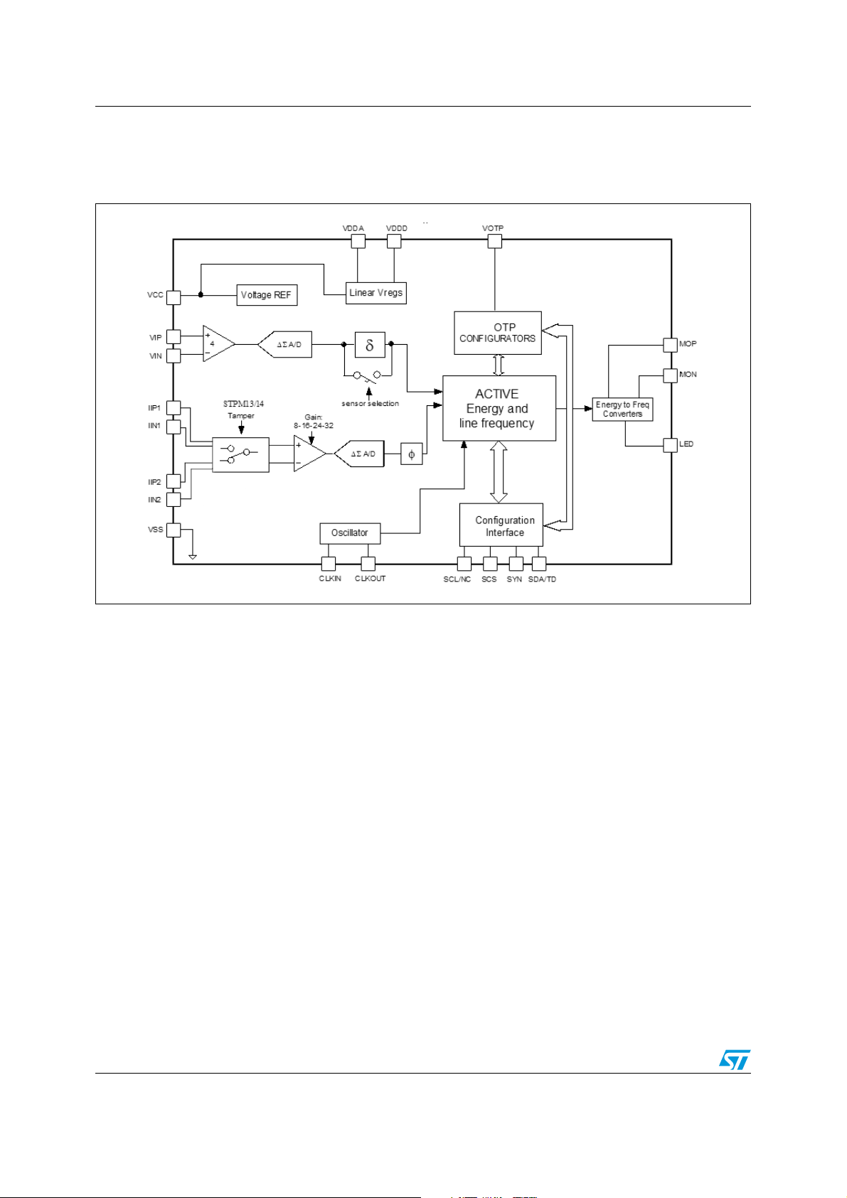
The STPM1x family is designed for effective
measurement of active energy in a power line
system using a Rogowski Coil, current
transformer and shunt sensors. This device is
specifically designed to provide all the necessary
features to implement a single phase energy
meter without any other active component. The
STPM1x device family consists, essentially, of two
parts: the analog part and the digital part. The
former, is composed of a preamplifier and first
order ∑ Δ A/D converter blocks, band gap voltage
reference, low drop voltage regulator. The digital
part is composed of a system control, oscillator,
hard wired DSP and interface for calibration and
STPM11, STPM12
STPM13, STPM14
and digital calibration
TSSOP20
configuration. The calibration and configuration
are done by OTP cells, that can be programmed
through a serial interface. The configured bits are
used for testing, configuration and calibration
purposes. From two ∑ Δ output signals coming
from the analog section, a DSP unit computes the
amount of consumed active energy. The active
energy is available as a pulse frequency output
and directly driven by a stepper counter. In the
STPM1x an output signal with pulse frequency
proportional to energy is generated. This signal is
used in the calibration phase of the energy meter
application allowing a very easy approach. When
the device is fully configured and calibrated, a
dedicated bit of OTP block can be written
permanently in order to prevent accidental entry
into test mode or changing any configuration bit.
Table 1. Device summary
Order codes Package Packaging
June 2011 Doc ID 13167 Rev 8 1/46
STPM11ATR TSSOP20 (tape and reel) 2500 parts per reel
STPM12ATR TSSOP20 (tape and reel) 2500 parts per reel
STPM13ATR TSSOP20 (tape and reel) 2500 parts per reel
STPM14ATR TSSOP20 (tape and reel) 2500 parts per reel
www.st.com
46

Contents STPM11, STPM12, STPM13, STPM14
Contents
1 Schematic diagram . . . . . . . . . . . . . . . . . . . . . . . . . . . . . . . . . . . . . . . . . 5
2 Pin configuration . . . . . . . . . . . . . . . . . . . . . . . . . . . . . . . . . . . . . . . . . . . 6
3 Maximum ratings . . . . . . . . . . . . . . . . . . . . . . . . . . . . . . . . . . . . . . . . . . . . 8
4 Electrical characteristics . . . . . . . . . . . . . . . . . . . . . . . . . . . . . . . . . . . . . 9
5 Terminology . . . . . . . . . . . . . . . . . . . . . . . . . . . . . . . . . . . . . . . . . . . . . . . 12
5.1 Measurement error . . . . . . . . . . . . . . . . . . . . . . . . . . . . . . . . . . . . . . . . . . 12
5.2 ADC offset error . . . . . . . . . . . . . . . . . . . . . . . . . . . . . . . . . . . . . . . . . . . . 12
5.3 Gain error . . . . . . . . . . . . . . . . . . . . . . . . . . . . . . . . . . . . . . . . . . . . . . . . . 12
5.4 Power supply DC and AC rejection . . . . . . . . . . . . . . . . . . . . . . . . . . . . . 12
5.5 Conventions . . . . . . . . . . . . . . . . . . . . . . . . . . . . . . . . . . . . . . . . . . . . . . . 12
6 Typical performance characteristics . . . . . . . . . . . . . . . . . . . . . . . . . . . 13
7 Theory of operation . . . . . . . . . . . . . . . . . . . . . . . . . . . . . . . . . . . . . . . . 15
7.1 General operation . . . . . . . . . . . . . . . . . . . . . . . . . . . . . . . . . . . . . . . . . . . 15
7.2 Analog inputs . . . . . . . . . . . . . . . . . . . . . . . . . . . . . . . . . . . . . . . . . . . . . . 15
7.3 ∑Δ A/D Converters . . . . . . . . . . . . . . . . . . . . . . . . . . . . . . . . . . . . . . . . . . 16
7.4 Period and line voltage measurement . . . . . . . . . . . . . . . . . . . . . . . . . . . 17
7.5 Single wire meter mode (STPM13/14 with Rogowsky coil sensor) . . . . . 18
7.6 Power supply . . . . . . . . . . . . . . . . . . . . . . . . . . . . . . . . . . . . . . . . . . . . . . 19
7.7 Load monitoring . . . . . . . . . . . . . . . . . . . . . . . . . . . . . . . . . . . . . . . . . . . . 20
7.8 Error detection . . . . . . . . . . . . . . . . . . . . . . . . . . . . . . . . . . . . . . . . . . . . . 21
7.9 Tamper detection module (STPM13/14 only) . . . . . . . . . . . . . . . . . . . . . . 21
7.10 Phase compensation . . . . . . . . . . . . . . . . . . . . . . . . . . . . . . . . . . . . . . . . 23
7.11 Clock generator . . . . . . . . . . . . . . . . . . . . . . . . . . . . . . . . . . . . . . . . . . . . 23
7.12 Resetting the STPM1x . . . . . . . . . . . . . . . . . . . . . . . . . . . . . . . . . . . . . . . 24
7.13 Energy to frequency conversion . . . . . . . . . . . . . . . . . . . . . . . . . . . . . . . . 24
7.14 Driving a stepper motor . . . . . . . . . . . . . . . . . . . . . . . . . . . . . . . . . . . . . . 25
7.15 Configuring the STPM1x . . . . . . . . . . . . . . . . . . . . . . . . . . . . . . . . . . . . . 26
2/46 Doc ID 13167 Rev 8

STPM11, STPM12, STPM13, STPM14 Contents
7.16 Mode signals . . . . . . . . . . . . . . . . . . . . . . . . . . . . . . . . . . . . . . . . . . . . . . 30
7.17 CFGI: configuration interface . . . . . . . . . . . . . . . . . . . . . . . . . . . . . . . . . . 30
8 Energy calculation algorithm . . . . . . . . . . . . . . . . . . . . . . . . . . . . . . . . . 34
9 STPM1x calibration . . . . . . . . . . . . . . . . . . . . . . . . . . . . . . . . . . . . . . . . . 37
10 Schematic . . . . . . . . . . . . . . . . . . . . . . . . . . . . . . . . . . . . . . . . . . . . . . . . 40
11 Package mechanical data . . . . . . . . . . . . . . . . . . . . . . . . . . . . . . . . . . . . 42
12 Revision history . . . . . . . . . . . . . . . . . . . . . . . . . . . . . . . . . . . . . . . . . . . 45
Doc ID 13167 Rev 8 3/46

List of tables STPM11, STPM12, STPM13, STPM14
List of tables
Table 1. Device summary . . . . . . . . . . . . . . . . . . . . . . . . . . . . . . . . . . . . . . . . . . . . . . . . . . . . . . . . . . 1
Table 2. Pin description . . . . . . . . . . . . . . . . . . . . . . . . . . . . . . . . . . . . . . . . . . . . . . . . . . . . . . . . . . . 7
Table 3. Absolute maximum ratings (see Note:). . . . . . . . . . . . . . . . . . . . . . . . . . . . . . . . . . . . . . . . . 8
Table 4. Thermal data. . . . . . . . . . . . . . . . . . . . . . . . . . . . . . . . . . . . . . . . . . . . . . . . . . . . . . . . . . . . . 8
Table 5. Electrical characteristics . . . . . . . . . . . . . . . . . . . . . . . . . . . . . . . . . . . . . . . . . . . . . . . . . . . . 9
Table 6. Typical external components . . . . . . . . . . . . . . . . . . . . . . . . . . . . . . . . . . . . . . . . . . . . . . . 11
Table 7. Voltage channel . . . . . . . . . . . . . . . . . . . . . . . . . . . . . . . . . . . . . . . . . . . . . . . . . . . . . . . . . 15
Table 8. Configuration of current sensors. . . . . . . . . . . . . . . . . . . . . . . . . . . . . . . . . . . . . . . . . . . . . 16
Table 9. Configuration of current sensors. . . . . . . . . . . . . . . . . . . . . . . . . . . . . . . . . . . . . . . . . . . . . 16
Table 10. RMS voltage check . . . . . . . . . . . . . . . . . . . . . . . . . . . . . . . . . . . . . . . . . . . . . . . . . . . . . . . 18
Table 11. Nominal voltage values. . . . . . . . . . . . . . . . . . . . . . . . . . . . . . . . . . . . . . . . . . . . . . . . . . . . 19
Table 12. No load detection thresholds . . . . . . . . . . . . . . . . . . . . . . . . . . . . . . . . . . . . . . . . . . . . . . . 20
Table 13. Different settings for led signal . . . . . . . . . . . . . . . . . . . . . . . . . . . . . . . . . . . . . . . . . . . . . . 25
Table 14. Configuration of MOP and MON pins . . . . . . . . . . . . . . . . . . . . . . . . . . . . . . . . . . . . . . . . . 25
Table 15. Configuration bits map . . . . . . . . . . . . . . . . . . . . . . . . . . . . . . . . . . . . . . . . . . . . . . . . . . . . 27
Table 16. Mode signals description . . . . . . . . . . . . . . . . . . . . . . . . . . . . . . . . . . . . . . . . . . . . . . . . . . 30
Table 17. Calibration entries . . . . . . . . . . . . . . . . . . . . . . . . . . . . . . . . . . . . . . . . . . . . . . . . . . . . . . . . 37
Table 18. Device calculation constants . . . . . . . . . . . . . . . . . . . . . . . . . . . . . . . . . . . . . . . . . . . . . . . 37
Table 19. Calibration results . . . . . . . . . . . . . . . . . . . . . . . . . . . . . . . . . . . . . . . . . . . . . . . . . . . . . . . . 38
Table 20. Document revision history . . . . . . . . . . . . . . . . . . . . . . . . . . . . . . . . . . . . . . . . . . . . . . . . . 45
4/46 Doc ID 13167 Rev 8

STPM11, STPM12, STPM13, STPM14 List of figures
List of figures
Figure 1. Block diagram . . . . . . . . . . . . . . . . . . . . . . . . . . . . . . . . . . . . . . . . . . . . . . . . . . . . . . . . . . . . 6
Figure 2. Pin connections (top view) . . . . . . . . . . . . . . . . . . . . . . . . . . . . . . . . . . . . . . . . . . . . . . . . . . 7
Figure 3. Supply current vs. supply voltage, T
Figure 4. RC oscillator frequency vs. V
CC
Figure 5. RC oscillator: frequency jitter vs. temperature . . . . . . . . . . . . . . . . . . . . . . . . . . . . . . . . . . 13
Figure 6. Analog voltage regulator: line - load regulation . . . . . . . . . . . . . . . . . . . . . . . . . . . . . . . . . 13
Figure 7. Digital voltage regulator: line - load regulation . . . . . . . . . . . . . . . . . . . . . . . . . . . . . . . . . . 13
Figure 8. Voltage channel linearity at different V
Figure 9. Power supply AC rejection vs. V
Figure 10. Power supply DC rejection vs. V
Figure 11. Error over dynamic range gain dependence. . . . . . . . . . . . . . . . . . . . . . . . . . . . . . . . . . . . 14
Figure 12. Primary current channel linearity at different V
Figure 13. Gain response of ΔΣ AD Converters. . . . . . . . . . . . . . . . . . . . . . . . . . . . . . . . . . . . . . . . . . 14
Figure 14. Clock frequency vs. external resistor . . . . . . . . . . . . . . . . . . . . . . . . . . . . . . . . . . . . . . . . . 14
Figure 15. First order ∑ Δ A/D converter . . . . . . . . . . . . . . . . . . . . . . . . . . . . . . . . . . . . . . . . . . . . . . . 17
Figure 16. Bandgap temperature variation . . . . . . . . . . . . . . . . . . . . . . . . . . . . . . . . . . . . . . . . . . . . . 20
Figure 17. Tamper conditions . . . . . . . . . . . . . . . . . . . . . . . . . . . . . . . . . . . . . . . . . . . . . . . . . . . . . . . 22
Figure 18. Different oscillator circuits (a); (b); (c) . . . . . . . . . . . . . . . . . . . . . . . . . . . . . . . . . . . . . . . . . 24
Figure 19. Positive energy stepper driving signals . . . . . . . . . . . . . . . . . . . . . . . . . . . . . . . . . . . . . . . 26
Figure 20. Negative energy stepper driving signals . . . . . . . . . . . . . . . . . . . . . . . . . . . . . . . . . . . . . . . 26
Figure 21. Timing for writing configuration and mode bits . . . . . . . . . . . . . . . . . . . . . . . . . . . . . . . . . . 32
Figure 22. Active energy computation diagram . . . . . . . . . . . . . . . . . . . . . . . . . . . . . . . . . . . . . . . . . . 34
Figure 23. Charge pump schematic. . . . . . . . . . . . . . . . . . . . . . . . . . . . . . . . . . . . . . . . . . . . . . . . . . . 40
Figure 24. Application schematic . . . . . . . . . . . . . . . . . . . . . . . . . . . . . . . . . . . . . . . . . . . . . . . . . . . . . 41
= 25 °C . . . . . . . . . . . . . . . . . . . . . . . . . . . . . . . . . . 13
A
, R = 12 kΩ, TA = 25 °C . . . . . . . . . . . . . . . . . . . . . . . . . . 13
voltages. . . . . . . . . . . . . . . . . . . . . . . . . . . . . . . 13
CC
. . . . . . . . . . . . . . . . . . . . . . . . . . . . . . . . . . . . . . . . . . . 14
CC
. . . . . . . . . . . . . . . . . . . . . . . . . . . . . . . . . . . . . . . . . . 14
CC
. . . . . . . . . . . . . . . . . . . . . . . . . . . . . . . . 14
CC
Doc ID 13167 Rev 8 5/46
Schematic diagram STPM11, STPM12, STPM13, STPM14
1 Schematic diagram
Figure 1. Block diagram
6/46 Doc ID 13167 Rev 8
STPM11, STPM12, STPM13, STPM14 Pin configuration
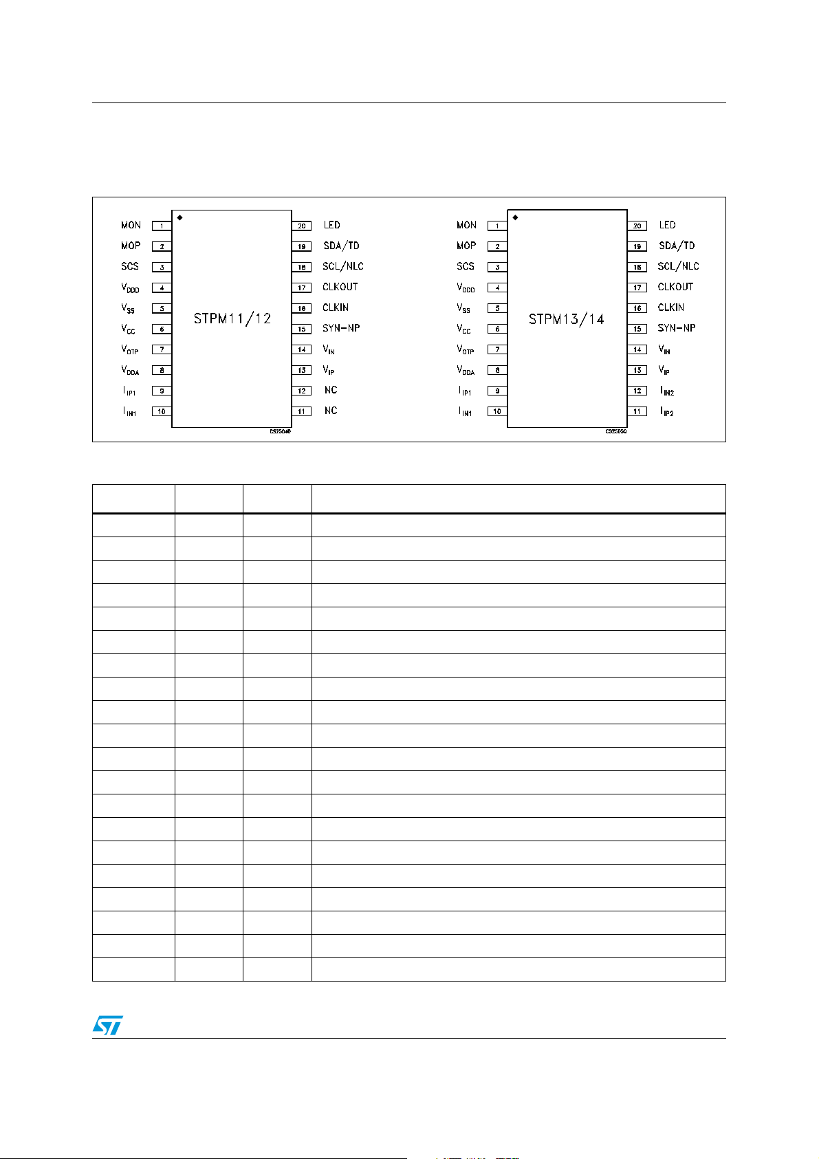
2 Pin configuration
Figure 2. Pin connections (top view)
Table 2. Pin description
Pin n° Symbol Type
(1)
Name and function
1 MON P O Output for Stepper’s node
2 MOP P O Output for Stepper’s node
3 SCS D IN Enable or disable configuration interface for device configuration.
4V
5V
6V
7V
8V
9I
10 I
11 I
12 I
13 V
14 V
DDD
SS
CC
OTP
DDA
IP1
IN1
IP2
IN2
IP
IN
A OUT 1.5 V Output of internal low drop regulator which supplies the digital core.
GND Ground.
P IN Supply voltage.
P INr Supply voltage for OTP cells.
A OUT 3 V output of internal low drop regulator which supplies the analog part.
A IN Positive input of primary current channel
A IN Negative input of primary current channel
A IN Positive input of secondary current channel (STPM13/14 only)
A IN Negative input of secondary current channel (STPM13/14 only)
A IN Positive input of voltage channel
A IN Negative input of voltage channel
15 SYN-NP D I/O Negative power indicator. (Configuration interface)
16 CLKIN A IN Crystal oscillator input or resistor connection if RC oscillator is selected
17 CLKOUT A OUT Oscillator output (RC or crystal)
18 SCL/NLC D I/O No-load condition indicator. (Configuration interface)
19 SDATD D I/O Tamper detection indicator. (Configuration interface)
20 LED D O Pulsed output proportional to active energy
1. A: Analog, D: Digital, P: Power
Doc ID 13167 Rev 8 7/46
Maximum ratings STPM11, STPM12, STPM13, STPM14
3 Maximum ratings
Table 3. Absolute maximum ratings (see Note:)
Symbol Parameter Value Unit
V
V
I
V
V
CC
PIN
ID
IA
OTP
DC input voltage -0.3 to 6 V
Current on any pin (sink/source) ± 150 mA
Input voltage at digital pins (SCS, MOP, MON, SYN, SDATD,
SCLNLC, LED)
Input voltage at analog pins (I
IP1
, I
, I
, I
IN1
, VIP, VIN) -0.7 to 0.7 V
IP2
IN2
-0.3 to V
+0.3 V
CC
Input voltage at OTP pin -0.3 to 25 V
ESD Human body model (all pins) ± 3.5 kV
Operating ambient temperature -40 to 85 °C
Junction temperature -40 to 150 °C
Storage temperature range -55 to 150 °C
T
T
T
STG
OP
J
Note: Absolute maximum ratings are those values beyond which damage to the device may occur.
Functional operation under these condition is not implied.
Table 4. Thermal data
Symbol Parameter Value Unit
R
thJA
Thermal resistance junction-ambient 114.5
1. This value is referred to single-layer PCB, JEDEC standard test board.
(1)
°C/W
8/46 Doc ID 13167 Rev 8
STPM11, STPM12, STPM13, STPM14 Electrical characteristics
4 Electrical characteristics
VCC = 5 V, TA= 25°C, 2.2 µF between V
between V
Table 5. Electrical characteristics
and VSS unless otherwise specified.
CC
and VSS, 2.2 µF between V
DDA
and VSS, 2.2 µF
DDD
Symbol Parameter Test conditions Min. Typ. Max. Unit
Energy measurement accuracy
f
e
Effective bandwidth Limited by digital filtering 5 400 Hz
BW
Accuracy of active power Over 1 to 1000 of dynamic range 0.1 %
AW
SNR Signal to noise ratio Over the entire bandwidth 52 db
rms
rms
/50Hz
/50 Hz
0.2 %
PSRR
Power supply DC rejection
DC
Voltage signal: 200mV
Current signal: 10mV
= 4.194 MHz VCC=3.3V±10%,
f
CLK
5 V±10%
Voltage signal:
200 mV
rms
/50 Hz
Current signal:
PSRRACPower supply AC rejection
10 mV
f
CLK
/50 Hz
rms
= 4.194 MHz,
VCC=3.3 V+0.2 V
=5.0 V+0.2 V
V
CC
1@100 Hz
rms
1@100 Hz
rms
0.1 %
General section
V
I
Operating supply voltage 3.0 5.5 V
CC
Supply current configuration
registers cleared or device
CC
locked (TSTD=1)
4 MHz, V
8 MHz, V
= 5 V 3.5 4
CC
= 5 V 4.7 6
CC
mA
Increase of supply current
per configuration bit, during
4 MHz, V
= 5 V 120
CC
programming
ΔI
CC
Increase of supply current
per configuration bit with
4 MHz, V
= 5 V 2
CC
µA/bit
device locked
POR Power on reset on V
V
V
Analog supply voltage 2.85 3.0 3.15 V
DDA
Digital supply voltage 1.425 1.50 1.575 V
DDD
CC
2.5 V
MDIV bit = 0 4.000 4.194 MHz
f
CLK
f
LINE
V
I
OTP
t
OTP
Oscillator clock frequency
MDIV bit = 1 8.000 8.192 MHz
Nominal line frequency 45 65 Hz
OTP programming voltage 14 20 V
OTP
OTP programming current
per bit
OTP programming time per
bit
100 300 µs
2.5 mA
Doc ID 13167 Rev 8 9/46
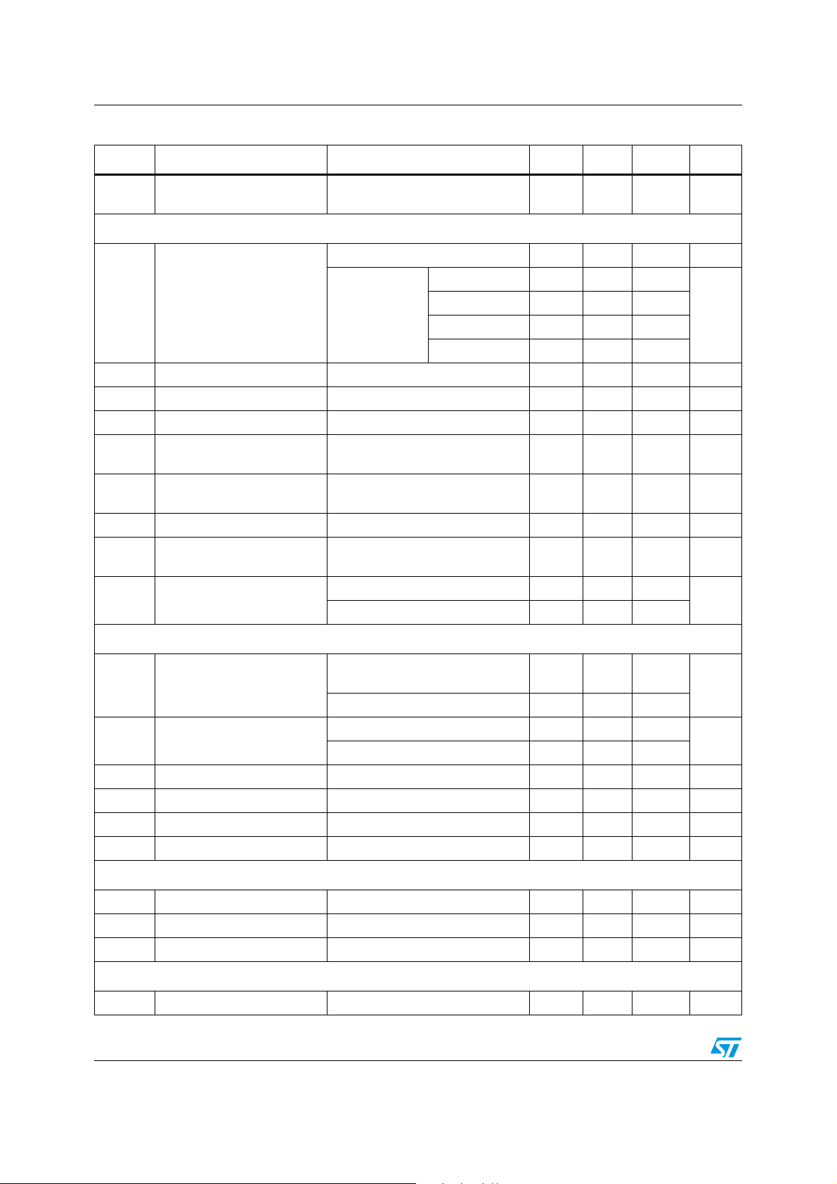
Electrical characteristics STPM11, STPM12, STPM13, STPM14
Table 5. Electrical characteristics (continued)
Symbol Parameter Test conditions Min. Typ. Max. Unit
I
LATCH
Current injection latch-up
immunity
Analog Inputs (I
V
f
ADC
f
SPL
V
Z
Z
G
I
I
LEAK
Maximum input signal levels
MAX
A/D Converter bandwidth 10 kHz
A/D Sampling frequency F
Amplifier offset ±20 mV
OFF
VIP, VIN Impedance
IP
V
IN
ERR
ILV
IP1
Impedance
Current channels gain error ±10 %
Voltage channel leakage
current
Current channel leakage
current
, V
IP1
IN1
, I
, V
IN1
IP2
300 mA
, I
, I
, VIP, VIN)
IP2
IN2
Voltage channel -0.3 0.3 V
Gain 8X -0.15 0.15
Current
channels
Gain 16X -0.075 0.075
V
Gain 24X -0.05 0.05
Gain 32X -0.035 0.035
/4 Hz
CLK
, V
IN2
Over the total operating voltage
range
Over the total operating voltage
range
100 400 kΩ
100 kΩ
-1 1 µA
Input disabled -1 1
µA
Input enabled -10 10
Digital I/O Characteristics (SDA-TD, CLKIN, CLKOUT, SCS, SYN-NP, LED)
SDA-TD, SCS, SYN-NP, LED
V
Input high voltage
IH
CLKIN 1.5
SDA-TD, SCS, SYN-NP, LED 0.25V
V
V
V
I
t
Input low voltage
IL
Output high voltage IO = -2 mA VCC-0.4 V
OH
Output low voltage IO = +2 mA 0.4 V
OL
Pull up current 15 µA
UP
Transition time C
TR
CLKIN 0.8
= 50 pF 10 ns
LOAD
Power I/O Characteristics (MOP, MON)
V
V
t
Output high voltage IO = -14 mA VCC-0.5 V
OH
Output low voltage IO = +14 mA 0.5 V
OL
Transition time C
TR
= 50 pF 5 10 ns
LOAD
Crystal oscillator (STPM12/14)
I
Input current on CLKIN ±1 µA
I
0.75V
C
C
V
CC
V
10/46 Doc ID 13167 Rev 8
STPM11, STPM12, STPM13, STPM14 Electrical characteristics
Table 5. Electrical characteristics (continued)
Symbol Parameter Test conditions Min. Typ. Max. Unit
R
C
f
CLK
External resistor 1 4 MΩ
P
External capacitors 22 pF
P
Nominal output frequency
RC Oscillator (STPM11/13)
I
CLKIN
R
t
Settling current
Settling resistor 12 kΩ
SET
Frequency jitter 1 ns
JIT
On chip reference voltage
Reference voltage 1.23 V
V
REF
Reference accuracy ±1 %
T
Temperature coefficient After calibration 30 50 ppm/°C
C
Configuration interface timing
F
SCLKw
t
t
t
SYN
Data write speed 100 kHz
Data setup time 20 ns
DS
Data hold time 0 ns
DH
SYN-NP active width 2/f
f
CLK
= 4 MHz
44.194
MHz
88.192
40 60 µA
CLK
s
Table 6. Typical external components
Function Component Parameter Value Tolerance Unit
Line voltage
interface
Line current
interface
Resistor divider
Current shunt
Rogowsky coil 3 ±12%
R to R ratio V
R to R ratio V
= 230 V 1650 ±1%
RMS
= 110 V 830 ±1%
RMS
0.2 ±5%
Current to voltage conversion ratio
Doc ID 13167 Rev 8 11/46
V/V
mV/ACurrent transformer 30 ±12%

Terminology STPM11, STPM12, STPM13, STPM14
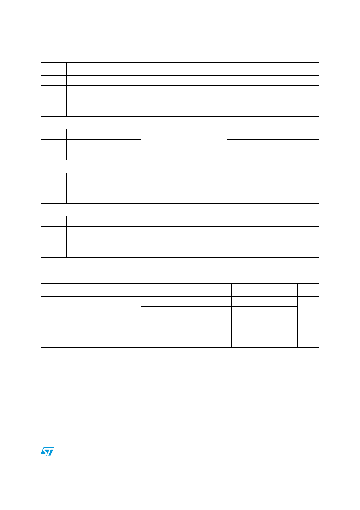
5 Terminology
5.1 Measurement error
The error associated with the energy measured by STPM1X is defined as:
Percentage Error = [STPM1X (reading) - True Energy] / True Energy
5.2 ADC offset error
This is the error due to the DC component associated with the analog inputs of the A/D
converters. Due to the internal automatic DC offset cancellation, the STPM1X measurement
is not affected by DC components in voltage and current channel. The DC offset
cancellation is implemented in the DSP.
5.3 Gain error
The gain error is gain due to the signal channel gain amplifiers. This is the difference
between the measured ADC code and the ideal output code. The difference is expressed as
a percentage of the ideal code.
5.4 Power supply DC and AC rejection
This parameter quantifies the STPM1X measurement error as a percentage of the reading
when the power supplies are varied. For the PSRR
nominal supply voltages (3.3 and 5 V) is taken. A second reading is obtained with the same
input signal levels when an ac (200 mV
RMS
voltages. Any error introduced by this ac signal is expressed as a percentage of reading.
For the PSRR
measurement, a reading at two nominal supply voltages (3.3 and 5 V) is
DC
taken. A second reading is obtained with the same input signal levels when the supplies are
varied ±10%. Any error introduced is again expressed as a percentage of the reading.
5.5 Conventions
The lowest analog and digital power supply voltage is named VSS which represents the
system Ground (GND). All voltage specifications for digital input/output pins are referred to
GND.
Positive currents flow into a pin. Sinking current means that the current is flowing into the pin
and is positive. Sourcing current means that the current is flowing out of the pin and is
negative.
The timing specifications of the signal treated by digital control are relative to CLKOUT. This
signal is provided by from the crystal oscillator of 4.194 MHz nominal frequency or by the
internal RC oscillator. An external source of 4.194 MHz or 8.192 MHz can be used.
measurement, a reading at two
AC
/100 Hz) signal is introduced onto the supply
The timing specifications of signals of the CFGI interface are relative to the SCL-NLC, there
is no direct relationship between the clock (SCL-NLC) of the CFGI interface and the clock of
the DSP block.
A positive logic convention is used in all equations.
12/46 Doc ID 13167 Rev 8

STPM11, STPM12, STPM13, STPM14 Typical performance characteristics
6 Typical performance characteristics
Figure 3. Supply current vs. supply voltage,
T
= 25 °C
A
Figure 5. RC oscillator: frequency jitter vs.
temperature
Figure 4. RC oscillator frequency vs. V
R = 12 kΩ, T
= 25 °C
A
CC
,
Figure 6. Analog voltage regulator: line - load
regulation
Figure 7. Digital voltage regulator: line - load
regulation
Figure 8. Voltage channel linearity at
different V
Doc ID 13167 Rev 8 13/46
voltages
CC

Typical performance characteristics STPM11, STPM12, STPM13, STPM14
Figure 9. Power supply AC rejection vs. V
CC
Figure 11. Error over dynamic range gain
dependence
Figure 10. Power supply DC rejection vs. V
CC
Figure 12. Primary current channel linearity at
different V
CC
Figure 13. Gain response of ΔΣ AD Converters Figure 14. Clock frequency vs. external
14/46 Doc ID 13167 Rev 8
8
7
6
5
f [MHz]
4
3
2
5101520
resistor
R [kΩ]
CRC=0
CRC=1
CRC=2
 Loading...