


Single phase energy metering IC with pulsed output
Features
■ Ripple free active energy pulsed output
■ Direct stepper counter drivers
■ Shunt, current transformer, Rogowsky coil
sensors
■ Live and neutral monitoring (STPM13/14)
■ Easy and fast digital calibration at only one
load point
■ No-load, negative power and tamper indicators
■ Integrated linear VREGs
■ RC (STPM11/13) or crystal oscillator
(STPM12/14)
■ Support 50 ÷ 60 Hz - IEC62052-11, IEC62053-
2X specification
■ Less than 0.1% error
Description
The STPM1x family is designed for effective
measurement of active energy in a power line
system using a Rogowski Coil, current
transformer and shunt sensors. This device is
specifically designed to provide all the necessary
features to implement a single phase energy
meter without any other active component. The
STPM1x device family consists, essentially, of two
parts: the analog part and the digital part. The
former, is composed of a preamplifier and first
order ∑ Δ A/D converter blocks, band gap voltage
reference, low drop voltage regulator. The digital
part is composed of a system control, oscillator,
hard wired DSP and interface for calibration and
STPM11, STPM12
STPM13, STPM14
and digital calibration
TSSOP20
configuration. The calibration and configuration
are done by OTP cells, that can be programmed
through a serial interface. The configured bits are
used for testing, configuration and calibration
purposes. From two ∑ Δ output signals coming
from the analog section, a DSP unit computes the
amount of consumed active energy. The active
energy is available as a pulse frequency output
and directly driven by a stepper counter. In the
STPM1x an output signal with pulse frequency
proportional to energy is generated. This signal is
used in the calibration phase of the energy meter
application allowing a very easy approach. When
the device is fully configured and calibrated, a
dedicated bit of OTP block can be written
permanently in order to prevent accidental entry
into test mode or changing any configuration bit.
Table 1. Device summary
Order codes Package Packaging
June 2011 Doc ID 13167 Rev 8 1/46
STPM11ATR TSSOP20 (tape and reel) 2500 parts per reel
STPM12ATR TSSOP20 (tape and reel) 2500 parts per reel
STPM13ATR TSSOP20 (tape and reel) 2500 parts per reel
STPM14ATR TSSOP20 (tape and reel) 2500 parts per reel
www.st.com
46

Contents STPM11, STPM12, STPM13, STPM14
Contents
1 Schematic diagram . . . . . . . . . . . . . . . . . . . . . . . . . . . . . . . . . . . . . . . . . 5
2 Pin configuration . . . . . . . . . . . . . . . . . . . . . . . . . . . . . . . . . . . . . . . . . . . 6
3 Maximum ratings . . . . . . . . . . . . . . . . . . . . . . . . . . . . . . . . . . . . . . . . . . . . 8
4 Electrical characteristics . . . . . . . . . . . . . . . . . . . . . . . . . . . . . . . . . . . . . 9
5 Terminology . . . . . . . . . . . . . . . . . . . . . . . . . . . . . . . . . . . . . . . . . . . . . . . 12
5.1 Measurement error . . . . . . . . . . . . . . . . . . . . . . . . . . . . . . . . . . . . . . . . . . 12
5.2 ADC offset error . . . . . . . . . . . . . . . . . . . . . . . . . . . . . . . . . . . . . . . . . . . . 12
5.3 Gain error . . . . . . . . . . . . . . . . . . . . . . . . . . . . . . . . . . . . . . . . . . . . . . . . . 12
5.4 Power supply DC and AC rejection . . . . . . . . . . . . . . . . . . . . . . . . . . . . . 12
5.5 Conventions . . . . . . . . . . . . . . . . . . . . . . . . . . . . . . . . . . . . . . . . . . . . . . . 12
6 Typical performance characteristics . . . . . . . . . . . . . . . . . . . . . . . . . . . 13
7 Theory of operation . . . . . . . . . . . . . . . . . . . . . . . . . . . . . . . . . . . . . . . . 15
7.1 General operation . . . . . . . . . . . . . . . . . . . . . . . . . . . . . . . . . . . . . . . . . . . 15
7.2 Analog inputs . . . . . . . . . . . . . . . . . . . . . . . . . . . . . . . . . . . . . . . . . . . . . . 15
7.3 ∑Δ A/D Converters . . . . . . . . . . . . . . . . . . . . . . . . . . . . . . . . . . . . . . . . . . 16
7.4 Period and line voltage measurement . . . . . . . . . . . . . . . . . . . . . . . . . . . 17
7.5 Single wire meter mode (STPM13/14 with Rogowsky coil sensor) . . . . . 18
7.6 Power supply . . . . . . . . . . . . . . . . . . . . . . . . . . . . . . . . . . . . . . . . . . . . . . 19
7.7 Load monitoring . . . . . . . . . . . . . . . . . . . . . . . . . . . . . . . . . . . . . . . . . . . . 20
7.8 Error detection . . . . . . . . . . . . . . . . . . . . . . . . . . . . . . . . . . . . . . . . . . . . . 21
7.9 Tamper detection module (STPM13/14 only) . . . . . . . . . . . . . . . . . . . . . . 21
7.10 Phase compensation . . . . . . . . . . . . . . . . . . . . . . . . . . . . . . . . . . . . . . . . 23
7.11 Clock generator . . . . . . . . . . . . . . . . . . . . . . . . . . . . . . . . . . . . . . . . . . . . 23
7.12 Resetting the STPM1x . . . . . . . . . . . . . . . . . . . . . . . . . . . . . . . . . . . . . . . 24
7.13 Energy to frequency conversion . . . . . . . . . . . . . . . . . . . . . . . . . . . . . . . . 24
7.14 Driving a stepper motor . . . . . . . . . . . . . . . . . . . . . . . . . . . . . . . . . . . . . . 25
7.15 Configuring the STPM1x . . . . . . . . . . . . . . . . . . . . . . . . . . . . . . . . . . . . . 26
2/46 Doc ID 13167 Rev 8

STPM11, STPM12, STPM13, STPM14 Contents
7.16 Mode signals . . . . . . . . . . . . . . . . . . . . . . . . . . . . . . . . . . . . . . . . . . . . . . 30
7.17 CFGI: configuration interface . . . . . . . . . . . . . . . . . . . . . . . . . . . . . . . . . . 30
8 Energy calculation algorithm . . . . . . . . . . . . . . . . . . . . . . . . . . . . . . . . . 34
9 STPM1x calibration . . . . . . . . . . . . . . . . . . . . . . . . . . . . . . . . . . . . . . . . . 37
10 Schematic . . . . . . . . . . . . . . . . . . . . . . . . . . . . . . . . . . . . . . . . . . . . . . . . 40
11 Package mechanical data . . . . . . . . . . . . . . . . . . . . . . . . . . . . . . . . . . . . 42
12 Revision history . . . . . . . . . . . . . . . . . . . . . . . . . . . . . . . . . . . . . . . . . . . 45
Doc ID 13167 Rev 8 3/46

List of tables STPM11, STPM12, STPM13, STPM14
List of tables
Table 1. Device summary . . . . . . . . . . . . . . . . . . . . . . . . . . . . . . . . . . . . . . . . . . . . . . . . . . . . . . . . . . 1
Table 2. Pin description . . . . . . . . . . . . . . . . . . . . . . . . . . . . . . . . . . . . . . . . . . . . . . . . . . . . . . . . . . . 7
Table 3. Absolute maximum ratings (see Note:). . . . . . . . . . . . . . . . . . . . . . . . . . . . . . . . . . . . . . . . . 8
Table 4. Thermal data. . . . . . . . . . . . . . . . . . . . . . . . . . . . . . . . . . . . . . . . . . . . . . . . . . . . . . . . . . . . . 8
Table 5. Electrical characteristics . . . . . . . . . . . . . . . . . . . . . . . . . . . . . . . . . . . . . . . . . . . . . . . . . . . . 9
Table 6. Typical external components . . . . . . . . . . . . . . . . . . . . . . . . . . . . . . . . . . . . . . . . . . . . . . . 11
Table 7. Voltage channel . . . . . . . . . . . . . . . . . . . . . . . . . . . . . . . . . . . . . . . . . . . . . . . . . . . . . . . . . 15
Table 8. Configuration of current sensors. . . . . . . . . . . . . . . . . . . . . . . . . . . . . . . . . . . . . . . . . . . . . 16
Table 9. Configuration of current sensors. . . . . . . . . . . . . . . . . . . . . . . . . . . . . . . . . . . . . . . . . . . . . 16
Table 10. RMS voltage check . . . . . . . . . . . . . . . . . . . . . . . . . . . . . . . . . . . . . . . . . . . . . . . . . . . . . . . 18
Table 11. Nominal voltage values. . . . . . . . . . . . . . . . . . . . . . . . . . . . . . . . . . . . . . . . . . . . . . . . . . . . 19
Table 12. No load detection thresholds . . . . . . . . . . . . . . . . . . . . . . . . . . . . . . . . . . . . . . . . . . . . . . . 20
Table 13. Different settings for led signal . . . . . . . . . . . . . . . . . . . . . . . . . . . . . . . . . . . . . . . . . . . . . . 25
Table 14. Configuration of MOP and MON pins . . . . . . . . . . . . . . . . . . . . . . . . . . . . . . . . . . . . . . . . . 25
Table 15. Configuration bits map . . . . . . . . . . . . . . . . . . . . . . . . . . . . . . . . . . . . . . . . . . . . . . . . . . . . 27
Table 16. Mode signals description . . . . . . . . . . . . . . . . . . . . . . . . . . . . . . . . . . . . . . . . . . . . . . . . . . 30
Table 17. Calibration entries . . . . . . . . . . . . . . . . . . . . . . . . . . . . . . . . . . . . . . . . . . . . . . . . . . . . . . . . 37
Table 18. Device calculation constants . . . . . . . . . . . . . . . . . . . . . . . . . . . . . . . . . . . . . . . . . . . . . . . 37
Table 19. Calibration results . . . . . . . . . . . . . . . . . . . . . . . . . . . . . . . . . . . . . . . . . . . . . . . . . . . . . . . . 38
Table 20. Document revision history . . . . . . . . . . . . . . . . . . . . . . . . . . . . . . . . . . . . . . . . . . . . . . . . . 45
4/46 Doc ID 13167 Rev 8

STPM11, STPM12, STPM13, STPM14 List of figures
List of figures
Figure 1. Block diagram . . . . . . . . . . . . . . . . . . . . . . . . . . . . . . . . . . . . . . . . . . . . . . . . . . . . . . . . . . . . 6
Figure 2. Pin connections (top view) . . . . . . . . . . . . . . . . . . . . . . . . . . . . . . . . . . . . . . . . . . . . . . . . . . 7
Figure 3. Supply current vs. supply voltage, T
Figure 4. RC oscillator frequency vs. V
CC
Figure 5. RC oscillator: frequency jitter vs. temperature . . . . . . . . . . . . . . . . . . . . . . . . . . . . . . . . . . 13
Figure 6. Analog voltage regulator: line - load regulation . . . . . . . . . . . . . . . . . . . . . . . . . . . . . . . . . 13
Figure 7. Digital voltage regulator: line - load regulation . . . . . . . . . . . . . . . . . . . . . . . . . . . . . . . . . . 13
Figure 8. Voltage channel linearity at different V
Figure 9. Power supply AC rejection vs. V
Figure 10. Power supply DC rejection vs. V
Figure 11. Error over dynamic range gain dependence. . . . . . . . . . . . . . . . . . . . . . . . . . . . . . . . . . . . 14
Figure 12. Primary current channel linearity at different V
Figure 13. Gain response of ΔΣ AD Converters. . . . . . . . . . . . . . . . . . . . . . . . . . . . . . . . . . . . . . . . . . 14
Figure 14. Clock frequency vs. external resistor . . . . . . . . . . . . . . . . . . . . . . . . . . . . . . . . . . . . . . . . . 14
Figure 15. First order ∑ Δ A/D converter . . . . . . . . . . . . . . . . . . . . . . . . . . . . . . . . . . . . . . . . . . . . . . . 17
Figure 16. Bandgap temperature variation . . . . . . . . . . . . . . . . . . . . . . . . . . . . . . . . . . . . . . . . . . . . . 20
Figure 17. Tamper conditions . . . . . . . . . . . . . . . . . . . . . . . . . . . . . . . . . . . . . . . . . . . . . . . . . . . . . . . 22
Figure 18. Different oscillator circuits (a); (b); (c) . . . . . . . . . . . . . . . . . . . . . . . . . . . . . . . . . . . . . . . . . 24
Figure 19. Positive energy stepper driving signals . . . . . . . . . . . . . . . . . . . . . . . . . . . . . . . . . . . . . . . 26
Figure 20. Negative energy stepper driving signals . . . . . . . . . . . . . . . . . . . . . . . . . . . . . . . . . . . . . . . 26
Figure 21. Timing for writing configuration and mode bits . . . . . . . . . . . . . . . . . . . . . . . . . . . . . . . . . . 32
Figure 22. Active energy computation diagram . . . . . . . . . . . . . . . . . . . . . . . . . . . . . . . . . . . . . . . . . . 34
Figure 23. Charge pump schematic. . . . . . . . . . . . . . . . . . . . . . . . . . . . . . . . . . . . . . . . . . . . . . . . . . . 40
Figure 24. Application schematic . . . . . . . . . . . . . . . . . . . . . . . . . . . . . . . . . . . . . . . . . . . . . . . . . . . . . 41
= 25 °C . . . . . . . . . . . . . . . . . . . . . . . . . . . . . . . . . . 13
A
, R = 12 kΩ, TA = 25 °C . . . . . . . . . . . . . . . . . . . . . . . . . . 13
voltages. . . . . . . . . . . . . . . . . . . . . . . . . . . . . . . 13
CC
. . . . . . . . . . . . . . . . . . . . . . . . . . . . . . . . . . . . . . . . . . . 14
CC
. . . . . . . . . . . . . . . . . . . . . . . . . . . . . . . . . . . . . . . . . . 14
CC
. . . . . . . . . . . . . . . . . . . . . . . . . . . . . . . . 14
CC
Doc ID 13167 Rev 8 5/46
Schematic diagram STPM11, STPM12, STPM13, STPM14
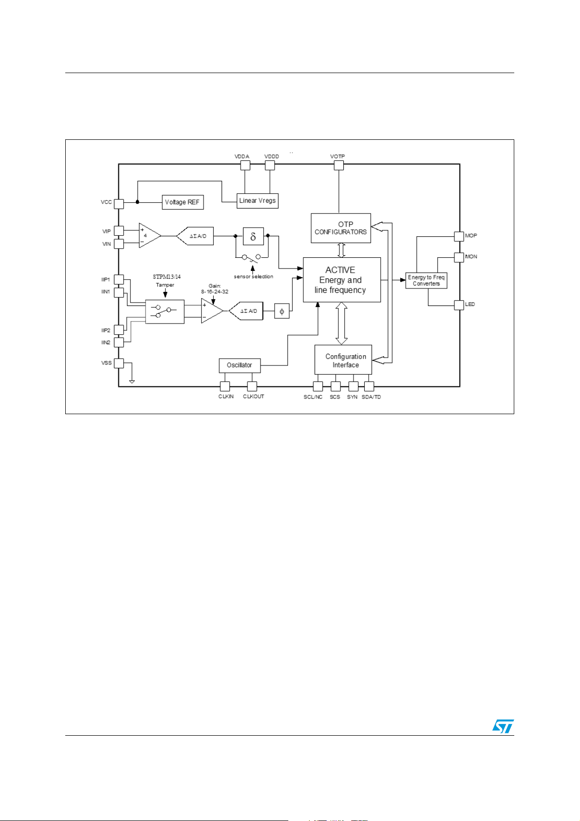
1 Schematic diagram
Figure 1. Block diagram
6/46 Doc ID 13167 Rev 8
STPM11, STPM12, STPM13, STPM14 Pin configuration
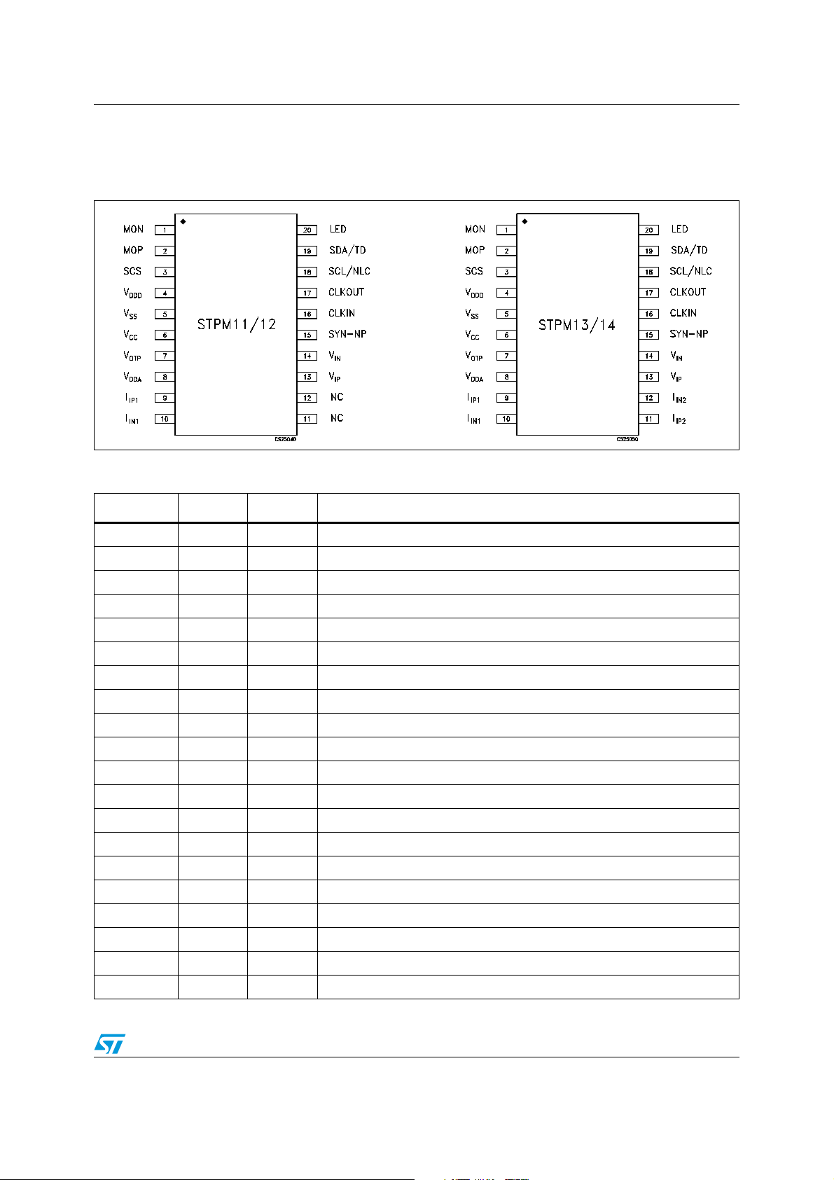
2 Pin configuration
Figure 2. Pin connections (top view)
Table 2. Pin description
Pin n° Symbol Type
(1)
Name and function
1 MON P O Output for Stepper’s node
2 MOP P O Output for Stepper’s node
3 SCS D IN Enable or disable configuration interface for device configuration.
4V
5V
6V
7V
8V
9I
10 I
11 I
12 I
13 V
14 V
DDD
SS
CC
OTP
DDA
IP1
IN1
IP2
IN2
IP
IN
A OUT 1.5 V Output of internal low drop regulator which supplies the digital core.
GND Ground.
P IN Supply voltage.
P INr Supply voltage for OTP cells.
A OUT 3 V output of internal low drop regulator which supplies the analog part.
A IN Positive input of primary current channel
A IN Negative input of primary current channel
A IN Positive input of secondary current channel (STPM13/14 only)
A IN Negative input of secondary current channel (STPM13/14 only)
A IN Positive input of voltage channel
A IN Negative input of voltage channel
15 SYN-NP D I/O Negative power indicator. (Configuration interface)
16 CLKIN A IN Crystal oscillator input or resistor connection if RC oscillator is selected
17 CLKOUT A OUT Oscillator output (RC or crystal)
18 SCL/NLC D I/O No-load condition indicator. (Configuration interface)
19 SDATD D I/O Tamper detection indicator. (Configuration interface)
20 LED D O Pulsed output proportional to active energy
1. A: Analog, D: Digital, P: Power
Doc ID 13167 Rev 8 7/46

Maximum ratings STPM11, STPM12, STPM13, STPM14
3 Maximum ratings
Table 3. Absolute maximum ratings (see Note:)
Symbol Parameter Value Unit
V
V
I
V
V
CC
PIN
ID
IA
OTP
DC input voltage -0.3 to 6 V
Current on any pin (sink/source) ± 150 mA
Input voltage at digital pins (SCS, MOP, MON, SYN, SDATD,
SCLNLC, LED)
Input voltage at analog pins (I
IP1
, I
, I
, I
IN1
, VIP, VIN) -0.7 to 0.7 V
IP2
IN2
-0.3 to V
+0.3 V
CC
Input voltage at OTP pin -0.3 to 25 V
ESD Human body model (all pins) ± 3.5 kV
Operating ambient temperature -40 to 85 °C
Junction temperature -40 to 150 °C
Storage temperature range -55 to 150 °C
T
T
T
STG
OP
J
Note: Absolute maximum ratings are those values beyond which damage to the device may occur.
Functional operation under these condition is not implied.
Table 4. Thermal data
Symbol Parameter Value Unit
R
thJA
Thermal resistance junction-ambient 114.5
1. This value is referred to single-layer PCB, JEDEC standard test board.
(1)
°C/W
8/46 Doc ID 13167 Rev 8

STPM11, STPM12, STPM13, STPM14 Electrical characteristics
4 Electrical characteristics
VCC = 5 V, TA= 25°C, 2.2 µF between V
between V
Table 5. Electrical characteristics
and VSS unless otherwise specified.
CC
and VSS, 2.2 µF between V
DDA
and VSS, 2.2 µF
DDD
Symbol Parameter Test conditions Min. Typ. Max. Unit
Energy measurement accuracy
f
e
Effective bandwidth Limited by digital filtering 5 400 Hz
BW
Accuracy of active power Over 1 to 1000 of dynamic range 0.1 %
AW
SNR Signal to noise ratio Over the entire bandwidth 52 db
rms
rms
/50Hz
/50 Hz
0.2 %
PSRR
Power supply DC rejection
DC
Voltage signal: 200mV
Current signal: 10mV
= 4.194 MHz VCC=3.3V±10%,
f
CLK
5 V±10%
Voltage signal:
200 mV
rms
/50 Hz
Current signal:
PSRRACPower supply AC rejection
10 mV
f
CLK
/50 Hz
rms
= 4.194 MHz,
VCC=3.3 V+0.2 V
=5.0 V+0.2 V
V
CC
1@100 Hz
rms
1@100 Hz
rms
0.1 %
General section
V
I
Operating supply voltage 3.0 5.5 V
CC
Supply current configuration
registers cleared or device
CC
locked (TSTD=1)
4 MHz, V
8 MHz, V
= 5 V 3.5 4
CC
= 5 V 4.7 6
CC
mA
Increase of supply current
per configuration bit, during
4 MHz, V
= 5 V 120
CC
programming
ΔI
CC
Increase of supply current
per configuration bit with
4 MHz, V
= 5 V 2
CC
µA/bit
device locked
POR Power on reset on V
V
V
Analog supply voltage 2.85 3.0 3.15 V
DDA
Digital supply voltage 1.425 1.50 1.575 V
DDD
CC
2.5 V
MDIV bit = 0 4.000 4.194 MHz
f
CLK
f
LINE
V
I
OTP
t
OTP
Oscillator clock frequency
MDIV bit = 1 8.000 8.192 MHz
Nominal line frequency 45 65 Hz
OTP programming voltage 14 20 V
OTP
OTP programming current
per bit
OTP programming time per
bit
100 300 µs
2.5 mA
Doc ID 13167 Rev 8 9/46

Electrical characteristics STPM11, STPM12, STPM13, STPM14
Table 5. Electrical characteristics (continued)
Symbol Parameter Test conditions Min. Typ. Max. Unit
I
LATCH
Current injection latch-up
immunity
Analog Inputs (I
V
f
ADC
f
SPL
V
Z
Z
G
I
I
LEAK
Maximum input signal levels
MAX
A/D Converter bandwidth 10 kHz
A/D Sampling frequency F
Amplifier offset ±20 mV
OFF
VIP, VIN Impedance
IP
V
IN
ERR
ILV
IP1
Impedance
Current channels gain error ±10 %
Voltage channel leakage
current
Current channel leakage
current
, V
IP1
IN1
, I
, V
IN1
IP2
300 mA
, I
, I
, VIP, VIN)
IP2
IN2
Voltage channel -0.3 0.3 V
Gain 8X -0.15 0.15
Current
channels
Gain 16X -0.075 0.075
V
Gain 24X -0.05 0.05
Gain 32X -0.035 0.035
/4 Hz
CLK
, V
IN2
Over the total operating voltage
range
Over the total operating voltage
range
100 400 kΩ
100 kΩ
-1 1 µA
Input disabled -1 1
µA
Input enabled -10 10
Digital I/O Characteristics (SDA-TD, CLKIN, CLKOUT, SCS, SYN-NP, LED)
SDA-TD, SCS, SYN-NP, LED
V
Input high voltage
IH
CLKIN 1.5
SDA-TD, SCS, SYN-NP, LED 0.25V
V
V
V
I
t
Input low voltage
IL
Output high voltage IO = -2 mA VCC-0.4 V
OH
Output low voltage IO = +2 mA 0.4 V
OL
Pull up current 15 µA
UP
Transition time C
TR
CLKIN 0.8
= 50 pF 10 ns
LOAD
Power I/O Characteristics (MOP, MON)
V
V
t
Output high voltage IO = -14 mA VCC-0.5 V
OH
Output low voltage IO = +14 mA 0.5 V
OL
Transition time C
TR
= 50 pF 5 10 ns
LOAD
Crystal oscillator (STPM12/14)
I
Input current on CLKIN ±1 µA
I
0.75V
C
C
V
CC
V
10/46 Doc ID 13167 Rev 8
STPM11, STPM12, STPM13, STPM14 Electrical characteristics
Table 5. Electrical characteristics (continued)
Symbol Parameter Test conditions Min. Typ. Max. Unit
R
C
f
CLK
External resistor 1 4 MΩ
P
External capacitors 22 pF
P
Nominal output frequency
RC Oscillator (STPM11/13)
I
CLKIN
R
t
Settling current
Settling resistor 12 kΩ
SET
Frequency jitter 1 ns
JIT
On chip reference voltage
Reference voltage 1.23 V
V
REF
Reference accuracy ±1 %
T
Temperature coefficient After calibration 30 50 ppm/°C
C
Configuration interface timing
F
SCLKw
t
t
t
SYN
Data write speed 100 kHz
Data setup time 20 ns
DS
Data hold time 0 ns
DH
SYN-NP active width 2/f
f
CLK
= 4 MHz
44.194
MHz
88.192
40 60 µA
CLK
s
Table 6. Typical external components
Function Component Parameter Value Tolerance Unit
Line voltage
interface
Line current
interface
Resistor divider
Current shunt
Rogowsky coil 3 ±12%
R to R ratio V
R to R ratio V
= 230 V 1650 ±1%
RMS
= 110 V 830 ±1%
RMS
0.2 ±5%
Current to voltage conversion ratio
Doc ID 13167 Rev 8 11/46
V/V
mV/ACurrent transformer 30 ±12%

Terminology STPM11, STPM12, STPM13, STPM14
5 Terminology
5.1 Measurement error
The error associated with the energy measured by STPM1X is defined as:
Percentage Error = [STPM1X (reading) - True Energy] / True Energy
5.2 ADC offset error
This is the error due to the DC component associated with the analog inputs of the A/D
converters. Due to the internal automatic DC offset cancellation, the STPM1X measurement
is not affected by DC components in voltage and current channel. The DC offset
cancellation is implemented in the DSP.
5.3 Gain error
The gain error is gain due to the signal channel gain amplifiers. This is the difference
between the measured ADC code and the ideal output code. The difference is expressed as
a percentage of the ideal code.
5.4 Power supply DC and AC rejection
This parameter quantifies the STPM1X measurement error as a percentage of the reading
when the power supplies are varied. For the PSRR
nominal supply voltages (3.3 and 5 V) is taken. A second reading is obtained with the same
input signal levels when an ac (200 mV
RMS
voltages. Any error introduced by this ac signal is expressed as a percentage of reading.
For the PSRR
measurement, a reading at two nominal supply voltages (3.3 and 5 V) is
DC
taken. A second reading is obtained with the same input signal levels when the supplies are
varied ±10%. Any error introduced is again expressed as a percentage of the reading.
5.5 Conventions
The lowest analog and digital power supply voltage is named VSS which represents the
system Ground (GND). All voltage specifications for digital input/output pins are referred to
GND.
Positive currents flow into a pin. Sinking current means that the current is flowing into the pin
and is positive. Sourcing current means that the current is flowing out of the pin and is
negative.
The timing specifications of the signal treated by digital control are relative to CLKOUT. This
signal is provided by from the crystal oscillator of 4.194 MHz nominal frequency or by the
internal RC oscillator. An external source of 4.194 MHz or 8.192 MHz can be used.
measurement, a reading at two
AC
/100 Hz) signal is introduced onto the supply
The timing specifications of signals of the CFGI interface are relative to the SCL-NLC, there
is no direct relationship between the clock (SCL-NLC) of the CFGI interface and the clock of
the DSP block.
A positive logic convention is used in all equations.
12/46 Doc ID 13167 Rev 8

STPM11, STPM12, STPM13, STPM14 Typical performance characteristics
6 Typical performance characteristics
Figure 3. Supply current vs. supply voltage,
T
= 25 °C
A
Figure 5. RC oscillator: frequency jitter vs.
temperature
Figure 4. RC oscillator frequency vs. V
R = 12 kΩ, T
= 25 °C
A
CC
,
Figure 6. Analog voltage regulator: line - load
regulation
Figure 7. Digital voltage regulator: line - load
regulation
Figure 8. Voltage channel linearity at
different V
Doc ID 13167 Rev 8 13/46
voltages
CC

Typical performance characteristics STPM11, STPM12, STPM13, STPM14
Figure 9. Power supply AC rejection vs. V
CC
Figure 11. Error over dynamic range gain
dependence
Figure 10. Power supply DC rejection vs. V
CC
Figure 12. Primary current channel linearity at
different V
CC
Figure 13. Gain response of ΔΣ AD Converters Figure 14. Clock frequency vs. external
14/46 Doc ID 13167 Rev 8
8
7
6
5
f [MHz]
4
3
2
5101520
resistor
R [kΩ]
CRC=0
CRC=1
CRC=2

STPM11, STPM12, STPM13, STPM14 Theory of operation
7 Theory of operation
7.1 General operation
The STPM1X is able to perform active energy measurement (wide band or fundamental) in
single-phase energy meter systems.
Due to the proprietary energy computation algorithm, STPM1X active energy is not affected
by any ripple at twice the line frequency. The calibration is very easy and fast allowing
calibration in only one point over the whole current range which allows saving time during
the calibration phase of the meter. The calibration parameters are permanently stored in the
OTP (one time programmable) cells, preventing calibration tampering.
Several functions are programmable using internal configuration bits accessible through the
configuration interface. The most important configuration bits are two configuration bits
called PST that allow the selection of the sensor and the gain of the input amplifiers.
The STPM1X is able to directly drive a stepper motor with the MOP and MON pins, and
provides information on tamper, no-load and negative power.
Two kinds of active energy can be selected to be brought to the LED pin: the total active
energy that includes all harmonic content in bandwidth or the active energy limited to the 1
harmonic only. This last energy value is obtained by filtering the wide band active energy.
7.2 Analog inputs
Input amplifiers
The STPM1X has one fully differential voltage input channel and one (STPM11/12) or two
(STPM13/14) fully differential current input channels.
The voltage channel consists of a differential amplifier with a gain of 4. The maximum
differential input voltage for the voltage channel is ± 0.3 V.
In STPM13/14, the two current channels are multiplexed (see tamper section for details) to
provide a single input to a preamplifier with a gain of 4. The output of this preamplifier is
connected to the input of a programmable gain amplifier (PGA) with possible gain selections
of 2, 4, 6, 8. The total gain of the current channels will be then 8, 16, 24, 32. The gain
selections are made by writing to the gain configuration bits PST and it can be different for
the two current channels. The maximum differential input voltage is dependent on the
selected gain according to the Tab le 7 :
Table 7. Voltage channel
Voltage channels Current channels
st
Gain Max input voltage (V) Gain Max input voltage (V)
8X ±0.15
4 ±0.30
16X ±0.075
24X ±0.05
32X ±0.035
Doc ID 13167 Rev 8 15/46

Theory of operation STPM11, STPM12, STPM13, STPM14
The Ta bl e 8 and Ta bl e 9 below show the gain values according to the configuration bits:
Table 8. Configuration of current sensors
STPM11/12
Current channel Configuration Bits
Gain Sensor PST (2bits) ADDG (1 bit)
8
00
16 0 1
Rogowsky Coil
24 1 0
32 1 1
8CT2x
32 Shunt 3 x
Table 9. Configuration of current sensors
STPM13/14
Primary Secondary Configuration Bits
Gain Sensor Gain Sensor PST (2bits) ADDG (1 bit)
8
8
00
16 16 0 1
Rogowsky Coil
Rogowsky Coil
24 24 1 0
32 32 1 1
8
8CT2 x
CT
8 32 Shunt 3 x
Both the voltage and current channels implement an active offset correction architecture
which has the benefit of avoiding any offset compensation.
The analog voltage and current signals are processed by the ∑ Δ Analog to digital
converters that feed the hardwired DSP. The DSP implements an automatic digital offset
cancellation that makes possible avoiding any manual offset calibration on the analog
inputs.
7.3 ∑Δ A/D Converters
The analog to digital conversion in the STPM1X is carried out using two first order ∑ Δ
converters. The device performs A/D conversions of analog signals on two independent
16/46 Doc ID 13167 Rev 8
channels in parallel. In STPM13/14, the current channel is multiplexed as primary or
secondary current channel in order to be able to perform a tamper function. The converted
∑ Δ signals are supplied to the internal hardwired DSP unit, which filters and integrates
those signals in order to boost the resolution and to yield all the necessary signals for
computations.
STPM11, STPM12, STPM13, STPM14 Theory of operation
A ∑ Δ modulator converts the input signal into a continuous serial stream of 1s and 0s at a
rate determined by the sampling clock. In the STPM1X, the sampling clock is equal to
f
/4. The 1-bit DAC in the feedback loop is driven by the serial data stream. The DAC
CLK
output is subtracted from the input signal. If the loop gain is high enough, the average value
of the DAC output (and therefore the bit stream) can approach that of the input signal level.
When a large number of samples are averaged, a very precise value of the analog signal is
obtained. This averaging is carried out in the DSP section which implements decimation,
integration and DC offset cancellation of the supplied ∑ Δ signals. The gain of the
decimation filters is 1.004 for the voltage channel and 0.502 for the current channel. The
resulting signal has a resolution of 11bits for voltage channel and 16 bits for current channel.
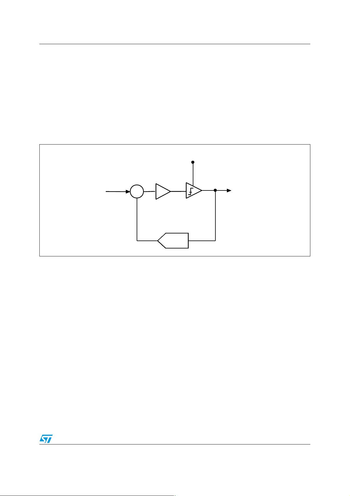
Figure 15. First order ∑ Δ A/D converter
f
/4
CLK
Integrator
Output digital signal
Input analog signal
+
Σ
∫
-
DAC
7.4 Period and line voltage measurement
The period module measures the period of base frequency of voltage channel and checks if
the voltage signal frequency is in the band from f
produced at every positive peak of the line voltage. If the counted number of pulses between
two trailing edges of this signal is higher than the f
counting is stopped (internal signal is not available), it means that the base frequency is
lower than f
If the counted number of pulses within one line period is higher than the f
pulses, the base frequency exceeds the limit. In this case, such error must be repeated
three times in a row, in order to set the error flag BFR.
The BFR flag is also set if the value of the RMS voltage drops below a certain value (BFRon) and it is cleared when the RMS voltage goes above BFR-off threshold. The table below
shows the equivalent RMS voltage on the V
channel calibrator.
The BFR flag is also set if the RMS voltage across V
calculated with the following formula:
/217 Hz and an internal error flag BFR (base frequency range) is set.
CLK
/217 to f
CLK
/217 Hz equivalent pulses or if the
CLK
pins according to the value of the voltage
IP/VIN
IP-VIN
/215. An internal signal is
CLK
/215 equivalent
CLK
drops below a threshold value
Doc ID 13167 Rev 8 17/46

Theory of operation STPM11, STPM12, STPM13, STPM14
Equation 1
V
BFRIRMS
−
64
=
K6703
⋅
V
(CT/Shunt)
Equation 2
V
BFRIRMS
−
64
=
K6687
⋅
V
(Rogowsky)
Where K
The BFR flag is cleared when the V
is the voltage calibrator value ranging from 0.875 to 1.000.
V
value goes above twice V
IRMS
IRMS-BFR
. When the BFR
error is set, the computation of power is suspended and MOP, MON and LED will be held
low.
Table 10. RMS voltage check
BFR-on BFR-off
Rogowsky 0.009571/Kv 0.019142/Kv
CT-Shunt 0.0078/Kv 0.0156/Kv
7.5 Single wire meter mode (STPM13/14 with Rogowsky coil sensor)
STPM1X supports the single wire meter (SWM) operation when working with Rogowsky
Coil current sensors. In SWM mode there is no available voltage information in the voltage
channel. It is possible that someone has disconnected one wire (live or neutral) of the meter
for tampering purposes or in case the line voltage is very stable, it is possible to use a
predefined value for computing the energy without sensing it.
In order to enable the SWM mode, the STPM1X must be configured with PST values of 0 or
1. In this way, if the BFR error is detected, STPM1X enters in SWM. If BFR is cleared, the
energy calculation is performed normally. When BFR is set (no voltage information is
available), the energy computation is carried out using a nominal voltage value according to
the NOM configuration bits.
Since there is no information on the phase shift between voltage and current, the apparent
rather than active power is used for tamper and energy computation. The calculated
apparent energy will be the product between I
V
that can be calculated as follows:
RMS
V
=VPK*K
RMS
STPM1X and K
18/46 Doc ID 13167 Rev 8
, where VPK represents the maximum line voltage reading of the
NOM
is a coefficient that changes according to Ta bl e 1 1 :
NOM
(effectively measured) and an equivalent
RMS

STPM11, STPM12, STPM13, STPM14 Theory of operation
Table 11. Nominal voltage values
NOM K
NOM
00.3594
10.3906
20.4219
30.4531
For example, if R1 = 783kΩ and R2 = 475Ω are used as resistor divider when the line
voltage is present, the positive voltage present at the input of the voltage channel of
STPM1x is:
Equation 3
R
VI
2
=
⋅
RR
+
21
RMS
2V
since the maximum voltage value applicable to the voltage channel input of STPM1x is
+0.3V, the equivalent maximum line voltage applicable is:
Equation 4
V
= R1+R2/R2 • 0.3 = 494.82
PK
considering the case of NOM=2, the correspondent RMS values used for energy
computation is:
Equation 5
V
= VPK • 0.4219 = 208.76 [V]
RMS
Usually the supply voltage for the electronic meter is taken from the line voltage. In SWM,
since the line voltage is no longer present, another power source must be used in order to
provide the necessary supply to STPM1x and the other electronic components of the meter.
7.6 Power supply
The main STPM1X supply pin is the VCC pin. From the VCC pin two linear regulators provide
the necessary voltage for the analog part V
The V
SS
should be connected between V
capacitors must be located very close to the device.
The STPM1X contains a power-on-reset (POR) detection circuit. If the V
than 2.5 V, then the STPM1X goes into an inactive state, all the functions are blocked
asserting and a reset condition is set. This is useful to ensure that the correct device
operation at power-up and during power-down. The power supply monitor has built-in
hysteresis and filtering, which give a high degree of immunity to false triggering due to noisy
supply voltages.
A bandgap voltage reference (VBG) of 1.23 V ±1% is used as reference voltage level source
for the two linear regulators and for the A/D converters. Also, this module produces several
(3 V) and for the digital part V
DDA
DDD
(1.5 V).
pin represents the reference point for all the internal signals. The 100nF capacitor
and VSS, V
CC
and VSS, V
DDA
and VSS. All these
DDD
supply is less
CC
Doc ID 13167 Rev 8 19/46

Theory of operation STPM11, STPM12, STPM13, STPM14
bias currents and voltages for all other analog modules and for the OTP module. The
bandgap voltage temperature behavior can be changed in order to better compensate the
variation of sensor sensitivity with temperature. This task is performed with the BGTC
configuration bits.
Figure 16. Bandgap temperature variation
7.7 Load monitoring
The STPM1X include a no-load condition detection circuit with adjustable threshold. This
circuit monitors the voltage and the current channels and, when the measured power is
below the set threshold, the internal signal BIL becomes high. The information about this
signal is also available in the status bit BIL.
The no load condition occurs when the product between V
below a given value. This value can be set with the LTCH configuration bits, and it is also
dependent on the selected current gain (Ai) and the calibration registers constant Kp=Kv*Ki.
Four different no-load threshold values can be chosen according to the two configurations
bits LTCH (see Ta bl e 1 2 ).
Table 12. No load detection thresholds
LTCH
0 0.004488 / (Ai*Kp) 0.003648 / (Ai*Kp)
1 0.008976 / (Ai*Kp) 0.007296 / (Ai*Kp)
2 0.017952 / (Ai*Kp) 0.014592 / (Ai*Kp)
3 0.035904 / (Ai*Kp) 0.029184 / (Ai*Kp)
V
* I
RMS
(input channel voltages) V
RMS
Rogowski coil (PST<2) Ct or Shunt (PST>1)
When a no-load condition occurs (BIL=1), the integration of power is suspended and the
tamper module is disabled.
RMS
and I
* I
RMS
RMS
RMS
(input channel voltages)
input values is
If a no-load condition is detected, the BIL signal blocks generation of pulses for stepper and
forces the SCLNLC pin to be low.
20/46 Doc ID 13167 Rev 8

STPM11, STPM12, STPM13, STPM14 Theory of operation
7.8 Error detection
In addition to the no-load condition and the line frequency band, the integration of power can
be suspended also due to detected error on the source signals.
There are two kinds of error detection circuits involved. The first checks all the ∑ Δ signals
from the analog part if any are stacked at 1 or 0 within the 1/128 of f
period of
CLK
observation. In case of detected error the corresponding ∑ Δ signal is replaced with an idle
∑ Δ signal, which represents a constant value 0.
Another error, condition occurs if the MOP, MON and LED pin outputs signals are different
from the internal signals that drive them. This can occur if some of this pin is forced to GND
or to some other imposed voltage value.
7.9 Tamper detection module (STPM13/14 only)
The STPM13/14 is able to measure the current in both live and neutral wires to implement
an anti-tamper function. When a difference between the two measurements is detected, the
STPM13/14 enters the tamper state. When there is a very small difference between the two
channels, the STPM13/14 is in normal state.
In particular, both channels are not constantly observed. A time multiplex mechanism is
used. During the observation time of the selected channel, its active energy is calculated.
The detection of a tamper condition occurs when the absolute value of the difference
between the two active energy values is greater than a certain percentage of the averaged
energy during the activated tamper module. This percentage value can be selected between
two different values (12.5% and 6.25%) according to the value of the configuration bit CRIT.
The tamper condition will be detected when the following formula is satisfied:
Equation 6
EnergyCH1 - EnergyCH2 > K
(EnergyCH1 + EnergyCH2)/2; where K
CRIT
can be 12.5%
CRIT
or 6.25%.
The detection threshold is much higher than the accuracy difference of the current channels,
which should be less than 0.1%. Some margin should be left for a possible transition effect,
due to accidental synchronism between the actual load current change and the rhythm of
taking the energy samples.
The tamper circuit works if the energies associated with the two current channels will be
both positive or both negative. If the two energies have different signs, the tamper remains
on constantly. However, the channel with the associated higher power is selected for the
final computation of energy.
In single wire mode, the apparent energy rather than active is used for tamper detection.
Detailed operational description
Normal state
The meter is initially set to normal state, i.e. tamper not detected. In such state, we expect
that the values of both load currents should not differ more than the accuracy difference of
the channels. For this reason, we can use an average value of currents of both channels for
the active energy calculation. The average is implemented with the multiplex ratio of 32:32
periods of line per channel. This means that for 32 periods of line voltage, i.e. 640 ms at 50
Hz, the current of the primary channel is used for the calculation followed by another 32
Doc ID 13167 Rev 8 21/46

Theory of operation STPM11, STPM12, STPM13, STPM14
periods of line voltage when the current of secondary channel is used instead. Four periods
before the primary to secondary switching point, a tamper detection module is activated. It is
deactivated after eight periods of line have elapsed. This means that energy of four periods
of primary channel immediately followed by energy of four periods of secondary channel is
sampled within the tamper module. We shall call those samples A and B respectively. From
these two samples the criteria of tamper detection is calculated. If four consecutive new
results of criteria happen, i.e. after elapsed 5.12s at 50 Hz, the meter will enter into tamper
state.
Tamper state
Within this state the multiplex ratio will change either to 60:4, when primary current is higher
than secondary, or to 4:60 otherwise. Thus, the channel with the higher current is used in
the energy calculation. The energy is not averaged by the mentioned ratio, rather the last
measured higher current is used also during 4 line period gap. The gap is still needed in
order to monitor the samples of the non-selected channel, which should check when the
tamper detected state is changed to either normal or another tamper detected state.
Several cases of transition of the state are shown in the Figure 17 - below
Figure 17. Tamper conditions
The detected tamper condition is stored in the BIT signal. This signal is connected to the
SDA-TD pin. When this pin is low, a tamper condition has been detected.
22/46 Doc ID 13167 Rev 8

STPM11, STPM12, STPM13, STPM14 Theory of operation
When internal signals are not good enough to perform the computation, i.e. line period is out
or range or ∑Δ signals from the analog part are stacked at high or low logic level, or no load
condition is activated, the tamper module is disabled and its state is preset to normal.
7.10 Phase compensation
The STPM1X is does not introduce any phase shift between voltage and current channels.
However, the voltage and current signals come from transducers, which could have inherent
phase errors. For example, a phase error of 0.1° to 0.3° is not uncommon for a current
transformer (CT). These phase errors can vary from part to part, and they must be corrected
in order to perform accurate power calculations. The errors associated with phase mismatch
are particularly noticeable at low power factors. The STPM1x provide a means of digitally
calibrating these small phase errors through a introducing delays on the voltage or current
signal. The amount of phase compensation can be set using the 4 bits of the phase
calibration register (CPH).
The default value of this register is at a value of 0 which gives 0° phase compensation. A
CPH value of 15 (1111) introduces a phase compensation of +0.576°. This compensates
the phase shift usually introduced by the current sensor, while the voltage sensor, normally
a resistor divider, does not introduce any delay. The resolution step of the phase
compensation is 0.038°.
7.11 Clock generator
All the internal timing of the STPM1X is based on the CLKOUT signal. This signal is
generated by different circuits according to the STPM1x version.
● STPM11/13: Internal RC Oscillator. A resistor connected between CLKIN and Ground
will set the RC current. For 4 MHz operation the suggested settling resistor is 12 kΩ;
The oscillator frequency can be compensated using the CRC configuration bit (see
Ta bl e 1 5 and Figure 14)
● STPM12/14: Quartz Oscillator. The oscillator circuit is designed to support an external
crystal. The suggested circuit is depicted in Figure 18. These versions support also an
external oscillator signal source that must be connected to the CLKOUT pin.
The clock generator is powered from analog supply and is responsible for two tasks. The
first one is to retard the turn-on of some function blocks after POR in order to help smooth
start of external power supply circuitry by keeping all major loads off.
The second task of the clock generator is to provide all necessary clocks for analog and
digital parts. Within this task, the MDIV configuration bit is used to inform the device about
the nominal frequency value of CLKOUT. The suggested operation frequency range is from
4.000 MHz to 4.194 MHz.
Doc ID 13167 Rev 8 23/46

Theory of operation STPM11, STPM12, STPM13, STPM14
Figure 18. Different oscillator circuits (a); (b); (c)
STPM12/14 with quartz
STPM11/13
7.12 Resetting the STPM1x
The STPM1x has no reset pin. The device is automatically reset by the POR circuit when
the V
crosses the 2.5 V value. When the reset occurs, all clocks and both DC buffers in
CC
the analog part are kept off for about 30 ms and all blocks of the digital part are held in a
reset state for about 125 ms after a reset condition.
Resetting the STPM1x causes all the functional modules of STPM1x to be cleared including
the OTP shadow latches (see 7.15 for OTP shadow latches description)
7.13 Energy to frequency conversion
The STPM1x provides energy to frequency conversion both for calibration and energy
readout purposes. In fact, one convenient way to verify the meter calibration is to provide a
pulse train signal with 50% duty cycle whose frequency signal is proportional to the active
energy under steady load conditions. It is convenient to have high frequency pulses during
calibration phase and low frequency for readout purposes; STPM1x supports both cases.
Let's suppose to choose a certain number of pulses on the LED pin (high frequency) that will
corresponds to 1 kWh. We will name this value as P.
The Active Energy frequency-based signal is available in the LED pin. The LED is driven
from internal signal AW (Active Energy) whose frequency is proportional to the active
energy. The desired P is achieved acting on the digital calibrators during the calibration
procedure.
STPM12/14 with external source
The APL configuration bit changes the internal divider that provides the signal on the LED
pin according to Ta bl e 1 3 , setting APL=1 the number of pulses are reduced in order to
provide low frequency pulses for readout purposes. The division factor is set according to
24/46 Doc ID 13167 Rev 8
KMOT configuration bits. In this case the pulses will have a fixed width of 31.25 ms.

STPM11, STPM12, STPM13, STPM14 Theory of operation
Table 13. Different settings for led signal
KMOT (2 Bits)
0
1 P/128
2 P/32
3 P/256
Due to the innovative and proprietary power calculation algorithm, the frequency signal is
not affected by any ripple at twice the line frequency. This feature strongly reduces the
calibration time of the meter.
7.14 Driving a stepper motor
The STPM1x is able to directly drive a stepper motor. An internal divider (mono-flop and
decoder) generates stepper driving signals MA and MB from signal AW. The MA and MB
signals are brought to the MOP and MON pins that are able to drive the stepper motor.
Several kinds of selections are possible for the driving signals according to the configuration
bits LVS and KMOT.
APL=0 APL=1
Pulses Pulses
P/64
P
The numbers of pulses per kWh (PM) in the MOP and MON outputs are linked with the
number of pulses of the LED P (see previous paragraph - 7.13) pin with the following
relationship.
Table 14. Configuration of MOP and MON pins
LVS (1 Bit) KMOT (2 Bits) Pulses length PM
0 0 31.25 ms P/64
0 1 31.25 ms P/128
0 2 31.25 ms P/32
0 3 31.25 ms P/256
1 0 156.25 ms P/640
1 1 156.25 ms P/1280
1 2 156.25 ms P/320
1 3 156.25 ms P/2560
The mono-flop limits the length of the pulses according to the LVS bit value.
The decoder distributes the pulses to MA and MB alternatively, which means that each of
them has only one half of selected frequency.
Negative power is computed with its own sign, and the MOP and MON signals invert their
logic state in order to make the backward rotation direction of the motor. See the diagram
below.
Doc ID 13167 Rev 8 25/46

Theory of operation STPM11, STPM12, STPM13, STPM14
Figure 19. Positive energy stepper driving signals
Hi
MON
Lo
Hi
MOP
Lo
Figure 20. Negative energy stepper driving signals
Hi
MON
Lo
Hi
Lo
When a no-load condition is detected MOP and MON are held low.
7.15 Configuring the STPM1x
All the configuration bits that control the operation of the device can be written temporarily or
permanently. For temporary writing, the configuration bits value are written in the shadow
registers which are simple latches that hold the configuration data. For permanent writing,
the configuration bits are stored in the OTP (one time programmable) cells that keep the
information for an undefined period of time even if the STPM1X is without supply, but, once
written, they cannot be changed. The temporary writing is useful mainly during testing of the
device or during the calibration phase. All the configuration parameters can be changed an
infinite number of times in order to test the device operation.
The shadow registers are cleared whenever a reset condition occurs.
The configuration bits are different for STPM11/12 and for STPM13/14 due to the presence
of the Tamper module. Each of them consists of paired elements, one is latch (the OTP
shadow), and one is the OTP antifuse element. When the STPM1X is released in the
market, all anti-fuses represent logic low state but they can be written by the user in order to
configure the STPM1X. This means that STPM1X can retain these bits of information even if
it has been unsupplied for an undefined time. That's why the CFG signals are used to keep
certain configuration and calibration values of the device.
MOP
26/46 Doc ID 13167 Rev 8

STPM11, STPM12, STPM13, STPM14 Theory of operation
The very first CFG bit, called TSTD, is used to disable any change of system signals after it
has been permanently set. During the configuration phase, each bit set to logic level 1
increases the supply current of STPM01 of about 120 µA, until the TSTD bit is set to 1. The
residual increase of supply current is 2 µA per each bit set to 1. It is then recommended to
set the TSTD bit to 1 after the configuration procedure in order to keep the supply current as
low as possible.
The STPM1x can work either using the data stored in the OTP cells or the data available in
the shadow latches. This can be chosen according to the value RD Mode signal (see
paragraph 7.16 for description). If the RD is set, the CFG bits originates from corresponding
OTP shadow latches. If the RD is cleared, the CFG bits originates from corresponding OTP
antifuses. In this way, it is possible to temporarily set up certain configurations or calibrations
of the device then verify and change, if necessary. This exercise is extensively used during
production tests.
Each configuration bit can be written sending a byte command to STPM1x through its
configuration interface. The procedure to write the configuration bits is described in the
Configuration Interface section (7.17).
After the TSTD bit has been set, no other command can be sent to the STPM1x. This
implies that the shadow latches can no longer be used as source of configuration data.
Table 15. Configuration bits map
Address
6-BIT
binary
DEC
000000 0 TSTD 1
000001 1 MDIV 1
000011 3 APL 1
000101 5
(1)
000110 6
Name
PST 2
N. of
bits
Description
(1)
Test mode and OTP write disable:
- TSTD=0: testing and continuous pre-charge of OTP when in read mode,
- TSTD=1:normal operation and no more writes to OTP
Measurement frequency range selection:
- MDIV=0: 4.000MHz to 4.194MHz,
- MDIV=1: 8.000MHz to 8.192MHz
LED pin frequency output:
- APL=0: P
- APL=1:
KMOT=0
KMOT=1
KMOT=2
KMOT=3
→ P/64
→ P/128
→ P/32
→ P/256
Current channel sensor type, gain and tamper selection:
STPM11/12
- PST=0: primary is Rogowsky coil x8 (x16 if ADDG=1)
- PST=1: primary is Rogowsky coil x24 (x32 if ADDG=1),
- PST=2: primary is CT x8,
- PST=3: primary is shunt x32,
STPM13/14
- PST=0: primary is Rogowsky coil x8 (x16 if ADDG=1), secondary is
Rogowsky coil x8 (x16 if ADDG=1),
- PST=1: primary is Rogowsky coil x24 (x32 if ADDG=1), secondary is
Rogowsky coil x24 (x32 if ADDG=1),
- PST=2: primary is CT x8, secondary is CT x8
- PST=3: primary is CT x8, secondary is shunt x32
Doc ID 13167 Rev 8 27/46

Theory of operation STPM11, STPM12, STPM13, STPM14
Table 15. Configuration bits map (continued)
Address
N. of
bits
6-BIT
binary
Name
DEC
This bit swaps the energy type between fundamental or wide band.
001010 10 FUND 1
- FUND=0: wide band active energy up to 50th harmonic;
- FUND=1: fundamental active energy
001011 11 1 Reserved
001100 12
No-load condition constant:
LTCH=0 → 800
001101 13
(1)
LT CH 2
LTCH=1
LTCH=2 → 3200
LTCH=3 → 6400
Constant of stepper pulses/kWh (see par. 7.14) selection:
If LVS=0,
001110 14
KMOT=0
KMOT=1
KMOT=2 → P/32
KMOT 2
KMOT=3
If LVS=1,
KMOT=0
KMOT=1
001111 15
(1)
KMOT=2 → P/320
KMOT=3 → P/2560
Description
→ 1600
→ P/64
→ P/128
→ P/256
→ P/640
→ P/1280
(1)
010010 18
010011 19
010100 20
010101 21
010110 22
010111 23
011000 24
011001 25
011010 26
011011 27
011100 28
011101 29
011110 30
011111 31
BGTC 2 Bandgap temperature compensation bits. See Figure 16 for details.
(1)
4-bit unsigned data for compensation of phase error, 0°+0.576°
CPH 4
16 values are possible with a compensation step of 0.0384°. When CPH=0
the compensation is 0°, when CPH=15 the compensation is 0.576°.
(1)
8-bit unsigned data for voltage channel calibration.
CHV 8
256 values are possible. When CHV is 0 the calibrator is at -12.5% of the
nominal value. When CHV is 255 the calibrator is at +12.5%. The calibration
step is then 0.098%.
(1)
28/46 Doc ID 13167 Rev 8

STPM11, STPM12, STPM13, STPM14 Theory of operation
Table 15. Configuration bits map (continued)
Address
6-BIT
binary
DEC
100000 32
100001 33
100010 34
100011 35
100100 36
100101 37
100110 38
100111 39
101000 40
101001 41
101010 42
101011 43
101100 44
101101 45
(1)
Name
CHP 8
CHS 8
N. of
bits
Description
8-bit unsigned data for primary current channel calibration.
256 values are possible. When CHP is 0 the calibrator is at -12.5% of the
nominal value. When CHP is 255 the calibrator is at +12.5%. The calibration
step is then 0.098%.
STPM13/14 only
8-bit unsigned data for secondary current channel calibration.
256 values are possible. When CHS is 0 the calibrator is at -12.5% of the
nominal value. When CHS is 255 the calibrator is at +12.5%. The calibration
step is then 0.098%.
(1)
101110 46
101111 47
110000 48
(1)
STPM11/13 only
2-bit unsigned data for calibration of RC oscillator. (see Typical characteristics
in)
CRC=0, or CRC=3 cal=0%
110001 49
(1)
CRC 2
CRC=1, cal=+10%;
CRC=2, cal=-10%
110010 50
NOM 2
110011 51
(1)
110100 52 ADDG 1
2-bit modifier of nominal voltage for Single Wire Meter.
NOM=0: K
NOM=3: K
=0.3594 / NOM=1: K
NOM
=0.4531
NOM
=0.3906 / NOM=2: K
NOM
Selection of additional gain on current channels:
ADDG=0: Gain+=0 / ADDG=1: Gain+=8
STPM13/14 only
110101 53 CRIT 1
Selection of tamper threshold:
CRIT =0: 12,5% / CRIT =1: 6,25%
110110 54 LVS 1
1. IMPORTANT: This Bit represents the MSB of the decimal value indicated in the description column.
Type of stepper selection:
LVS=0: pulse width 31.25 ms, 5V, / LVS=1: pulse width, 156.25 ms, 3V
NOM
=0.4219 /
Doc ID 13167 Rev 8 29/46

Theory of operation STPM11, STPM12, STPM13, STPM14
7.16 Mode signals
The STPM1x includes four mode signals. These signals change some of the operation of
the STPM1x. The mode signals are not retained when the STPM1x supply is not available
and then they are cleared when a POR occurs.
The mode signals bit can be written using the normal writing procedure of the CFGI
interface (see CFGI par. 7.17)
Table 16. Mode signals description
Signal
Name
PUMP
RD
WE
Bit
Val ue
Status
Binary
Command
Hex
Command
0 MOP and MON operate normally 0111001x 72 or 73
MOP and MON provide the driving signals to implement a
1
charge-pump DC-DC converter
1111001x F2 or F3
0 The 56 Configuration bits originated by OTP anti-fuses 0111101x 7A or 7B
1 The 56 Configuration bits originated by shadow latches 1111101x FA or FB
Any writing in the configuration bits is recorded in the shadow
0
latches
Any writing in the configuration bits is recorded both in the
1
shadow latches and in the OTP anti-fuse elements
0111110x 7C or 7D
1111110x FC or FD
– RD mode signal has been already described in par. 7.15 (configuring the STPM1x),
but there is another implied function of the signal RD. When it is set, each sense
amplifier is disconnected from corresponding antifuse element and this way, its 3 V
NMOS gate is protected from the high voltage of V
operation. This means that as long as the V
voltage reads more than 3 V, the
OTP
during permanent write
OTP
signal RD should be set.
– PUMP. When set, the PUMP mode signal transforms the MOP and MON pins to act
as driving signals to implement a charge-pump DC-DC converter (see Figure 23).
This feature is useful in order to boost the V
generate the V
voltage (14 V to 20 V) needed to program the OTP anti-fuse
OTP
supply voltage of the STPM1x to
CC
elements.
– WE (write Enable): This mode signal is used to permanently write to the OTP anti-
fuse element. When this bit is not set, any writing to the configuration bit is recorded
in the shadow latches. When this bit is set, the writing is recorded both in the shadow
latch and in the OTP anti-fuse element.
7.17 CFGI: configuration interface
The CFGI interface supports a simple serial protocol, which is implemented in order to
enable the configuration of STPM1x which allows writing the mode bits and the
configuration bits (temporarily or permanently);
30/46 Doc ID 13167 Rev 8
Four pins of the device are dedicated to this purpose: SCS, SYN-NP, SCLNCN, SDATD.
SCS, SYN-NP, SCL-NLC and SDATD are all input pins. A high level signal for these pins
means a voltage level higher than 0.75 x V
lower than 0.25 x V
CC
.
, while a low level signal means a voltage value
CC

STPM11, STPM12, STPM13, STPM14 Theory of operation
The condition in which SCS, SYN-NP and SCL-NLC inputs are set to high level determines
the idle state of the CFGI interface and no data transfer occurs.
– SCS: in the STPM1X, the SYN-NP, SCL-NLC and SDA-TD have the dual task to
provide information on the meter status (see Pin Description table) and to allow CFGI
communication. The SCS pin allows using the above pins for CFGI communication
when it is low and allows the normal operation of SYN-NP, SCL-NLC and SDA-TD
when it is high. In this section, the SYN-NP, SCL-NLC and SDA-TD operation as part
of the CFGI interface is described.
– SYN-NP: this pin allows synchronization of the communication between STPM1x and
the host. See Figure 21 - for detailed timing of the pin.
– SCL-NLC: it is basically the clock pin of the CFGI interface. This pin function is also
controlled by the SCS status. If SCS is low, SCL-NLC is the input of the serial bit
synchronization clock signal. When SCS is high, SCL-NLC is also high which
determines the idle state of the CFGI.
– SDA-TD is the Data pin. SDA-TD is the input of the serial bit data signal.
Any pin above has internal weak pull up device of nominal 15 A. This means that when a pin
is not forced by external signals, the state of the pin is logic high. A high state of any input
pin above is considered as an idle (not active) state. For the CFGI to operate correctly, the
STPM1x must be correctly supplied as described in the power supply section. When SCS is
active (low), signal SDA-TD should change its state at trailing edge of signal SCL-NLC and
the signal SDA-TD should be stable at the next leading edge of signal SCL-NLC. The first
valid bit of SDA-TD always starts with the activation of signal SCL-NLC.
Writing procedure
Each writable bit (configuration and mode bits) has its own 6-bit absolute address. For the
configuration bits, the 6-bit address value corresponds to its decimal value, while for the
mode bits, the addresses are the ones indicated in the Mode Signal paragraph (7.16).
In order to change the latch state, a byte of data must be sent to STPM1x via CFGI. This
byte consists of 1-bit data to be latched (msb), followed by 6-bit address of destination latch,
followed by 1-bit don't care data (lsb) which totals 8 bits of command byte.
For example, if we would like to set the configuration bit 52 (additional gain of 8) to 1, we
must convert the decimal 52 to its 6-bit binary value: 110100. The byte command will be
then composed like this:
1 bit DATA value+6-bits address+1 bit (0 or 1) as depicted in Figure 21. In this case the
binary command will be 11101000 (0xE8) or 11101001 (0xE9).
Doc ID 13167 Rev 8 31/46

Theory of operation STPM11, STPM12, STPM13, STPM14
Figure 21. Timing for writing configuration and mode bits
t1 → t2 (>30ns): CFGI out of idle state
t
→ t3 (>30ns): CFGI enabled for write operation
2
t
: data value is placed in SDA
3
t4: SDA value is stable and shifted into the device
t
→ t5 (>10µs): writing Clock period
3
t
→ t5: 1 bit Data value
3
t
→ t6: 6 bits address of the destination latch
5
t
→ t7: 1 bit EXE command
6
t
: end of CFGI writing
8
t
: CFGI enters idle state
9
The same procedure should be applied for the mode signals, but in this case the 6-bits
address must be taken from the Ta bl e 1 5 .
The lsb of command is also called EXE bit because instead of data bit value, the
corresponding serial clock pulse is used to generate the necessary latching signal. In this
way the writing mechanism does not need the measurement clock in order to operate, which
makes the operation of CFGI module of STPM1x completely independent from the rest of
the device logic except from the signal POR.
Commands for changing system signals should be sent during active signals SCS and SYNNP as it is shown in the Figure 21 -. A string of commands can be send within one period of
active signals SCS and SYN-NP.
32/46 Doc ID 13167 Rev 8

STPM11, STPM12, STPM13, STPM14 Theory of operation
Permanent writing of the CFG bits
In order to make a permanent set of some CFG bits, use the following procedure:
1. collect all addresses of CFG bits to be permanently set into a list;
2. clear all OTP shadow latches;
3. set the system signal RD;
4. connect a current source of at least +14 V, 1 mA to 3 mA to VOTP;
5. wait for VOTP voltage to be stable;
6. set one OTP shadow latch from the list;
7. set the system signal WE;
8. wait for 300 s;
9. clear the system signal WE;
10. clear the OTP shadow latch which was set in step 6;
11. until all CFG bits are permanently set as desired, repeat steps 5 to 11;
12. disconnect the current source;
13. wait for VOTP voltage to be less than 3 V;
14. clear the system signal RD;
15. verify the correct writing, testing STPM1x operation;
16. if the verification of CFG bits fails, repeat steps 1 to 16.
For steps of set or clear, apply the timing shown in Figure 21 - with proper signal on the
SDA-TD.
In order to create a permanent set of the TSTD bit, which does not result in any more writing
to the Configuration bits, the procedure above must be conducted in such a way that steps 6
to 13 are performed in series during a single period of active SCS. The idle state of SCS
would make the signal TSTD immediately effective which in turn, would abort the procedure
and possibly destroy the device due to clearing of system signal RD. This would result in the
connecting of all gates of 3 V NMOS sense amplifiers of already permanently set CFG bits
to the V
OTP
source.
Doc ID 13167 Rev 8 33/46

Energy calculation algorithm STPM11, STPM12, STPM13, STPM14
8 Energy calculation algorithm
Inside the STPM1x the computing section of the measured active power uses a completely
new patented signal process approach. This approach allows the device to reach high
performances in terms of accuracy.
The signals, coming from the sensors, for the instantaneous voltage is:
Equation 7
v(t) = V•sin ωt; where V is the peak voltage and ω is related to the line frequency
and the instantaneous current is:
Equation 8
i(t) = I • sin (ωt + ϕ); where I is the peak current, ω is related to the line frequency and ϕ is
the phase difference between voltage and current
Active power
Figure 22. Active energy computation diagram
34/46 Doc ID 13167 Rev 8

STPM11, STPM12, STPM13, STPM14 Energy calculation algorithm
In the STPM1x, after the pre-conditioning and the A/D conversion, the digital voltage signal
(which is dynamically more stable with respect to the current signal) is processed by a
differentiate stage which transforms:
Equation 9
v(t) → v’(t) = dv/dt = V
⋅ ω ⋅ cos tω; (see [5] in Figure 22);
The result, together with the pre-processed and digitalized current signal:
Equation 10
i(t) = I
⋅ sin (tω + ϕ); (see [6] in Figure 22)
can then be used to calculate. These digital signals are also used in two additional steps for
integration, obtaining:
Equation 11
dv/dt → v(t) = V
⋅ sin tω; (see [7] in Figure 22)
Equation 12
i(t) ⋅
∫
dt)t(i)t(I ϕ+ω⋅
I
−=⋅=
ω
)tcos(
(see [8] in Figure 22)
Now four signals are available. Combining (pairing) them by two multiplication steps two
results are obtained:
Equation 13
ϕ⋅⋅
dv
)t(p
/
1
dt
∫
−=⋅⋅=
dt)t(i
cosIV
2
−
2
ϕ+ω⋅⋅
)t2cos(IV
(see [9] in Figure 22)
Equation 14
ϕ⋅⋅
cosIV
=⋅=
/
2
)t(i)t(v)t(p
2
−
2
ϕ+ω⋅⋅
)t2cos(IV
(see [10] in Figure 22)
After these two operations, another stage another step involves the subtraction of p1 from
p2 and dividing the result by 2, to obtain the active power:
Equation 15
=
)t(p
−
))t(p)t(p(
/
/
12
=
2
ϕ⋅⋅
cosIV
2
(see [12] in Figure 22)
In this way, the AC part
Doc ID 13167 Rev 8 35/46

Energy calculation algorithm STPM11, STPM12, STPM13, STPM14
Equation 16
ϕ+ω⋅⋅
)t2cos(IV
⎛
⎜
⎝
2
⎞
⎟
⎠
has been then removed from the instantaneous power.
In the case of current sensors like "Rogowski coils", which provide the rate of the
instantaneous current signal, the initial voltage signal differentiation stage is switched off. In
this case the signals coming from the A/D conversion and their consequent integrations are:
Equation 17
v(t) = V
⋅ sin (tω);
Equation 18
′
)t(i ϕ+ω⋅ω⋅−==
)t(di
)tcos(I
dt
Equation 19
V
−=⋅=
ω
∫
dt)t(v)t(V ω⋅
Equation 20
′′
′
=
∫
The signals process flow is the same as shown in the previous case, and even with the
formulas above, the result is the same.
The absence of any AC component allows a very fast calibration procedure. Averaging the
readings of several line periods is not needed. The active energy measurement is already
stable after one line cycle. Moreover the digital calibration allows saving time and space
compared to the hardware calibration made with resistor strings.
tcos
)tsin(I)t(idt)t(i)t(i ϕ+ω⋅−==⋅
36/46 Doc ID 13167 Rev 8

STPM11, STPM12, STPM13, STPM14 STPM1x calibration
9 STPM1x calibration
Energy meters based on STPM1x devices are calibrated on the frequency of the output
pulse signal.
The devices are comprised of two independent meter channels for line voltage and current
respectively. Each channel includes its own digital calibrator, to adjust the voltage and
current signals coming from the sensors in the range of ±12.5% in 256 steps. A digital filter
is included to remove any signal DC component.
The devices produce an energy output pulse signal whose frequency is proportional to the
measured active energy.
The devices have an embedded memory, 54 bits, used for configuration and calibration
purposes. The value of these bits can be written temporarily or permanently through CFGI
communication channel.
The basic information needed to start the calibration procedure is found in Ta bl e 1 7 and
Ta bl e 1 8 :
Table 17. Calibration entries
Symbol Description Value
Vn Line RMS voltage (230 V)
In Line RMS current (5 A)
P Power sensitivity (LED: P=128000 pulses/kWh, Stepper Motor: PM=P/64= 2000 pulses/kWh)
Si Shunt Sensor 0,42 mV/A
The following typical STPM01 parameters and constants are also known:
Table 18. Device calculation constants
Symbol Description Value
Vbg Reference voltage (1.23 V ± 2%)
fM Clock (223 Hz ± 50ppm)
Av, Ai Amplification of ADC [4 ± 1%, (8, 16, 24, 32) ± 2%)]
Gp Gain of voltage and current decimation filters (0.504008)
Cv, Ci Calibration data range (min = 0, ini = 128, max = 255)
DL AW Bit position that generates LED signal (2
11
)
Av is constant. While, Ai is chosen according to the sensor
Gv and Gi are constant
Cv and Ci are 8bits register (CHV, CHP and CHS)
From the values above and for both the given amplification factor and initial calibration data,
the following target values can be calculated:
Considering that Ci=0 generates a correction of 75% and that Ci=128 determines a
correction factor of 87.5%, and the same for Cv, the total correction for the power stands
Doc ID 13167 Rev 8 37/46

STPM1x calibration STPM11, STPM12, STPM13, STPM14
within Kp = Kv*Ki = (0.75*0.75)=56.25% and 100%, and Cv=Ci=128 gives a correction
factor of Kp= (0.875*0.875) = 76.5625%.
Each calibrator value can be changed from a binary form to a decimal correction form, using
the following formula:
Kv=(Cv/128)*0.125 + 0.75 and the same for Ki.
Let us choose as initial value Ai=32
Table 19. Calibration results
Value of Calibrator Kp = Kv*Ki = 0.765625
Frequency at LED f = P*In*Vn/3600000 = 40.8889 Hz
Voltage divider Sv = (F*DL*Vbg
Voltage divider resistor R1=R2*(1000/Sv-1)
Description Value
2
)/(fM*Vn*In*Gv*Gi*Kp*Ai*Av*Si)= 0,6324mV/V
From the target power constant CP of the meter and the actual values of V
RMS
and I
RMS
,
which are applied to the meter under calibration, the error of power measurement can be
calculated:
Equation 21
err = 100(fx/f -1) [%], where fx is the real frequency read at LED output.
Now, a final unit less power reduction factor can be calculated:
Equation 22
p
= (pD - err)/100
F
This final power reduction factor can be considered as a product of voltage and current
reduction factors which are produced from corresponding calibration constants. So, an
obvious solution to obtain the voltage and current reduction factors is to calculate a common
reduction factor as a square root of pF. This result must fall within the indicated range,
otherwise the device cannot be calibrated:
768 ≤ R = 1024 pF + 0.125 < 1024
In order to obtain the corresponding calibration constants, the reduction factor must be
transformed:
CV = CC = R - 768
By using separately the integer and the fractional part of the common reduction a better fit of
calibration constants can be produced. Simply, let's set one of the two calibration registers
(e.g. CV) to the lowest integer value of R, while the other (CC) should be set to the nearest
integer value of R. Examples:
R-768=128.124; in this case set CV=128; set CC=128
38/46 Doc ID 13167 Rev 8
R-768=127.755; while in this other one set CV=127; set CC=128.

STPM11, STPM12, STPM13, STPM14 STPM1x calibration
Note: STPM13/14: each current channel must be calibrated separately. In order to do this, follow
these steps:
Apply the nominal test voltage to the voltage sensor, and the nominal test current to the
primary current channel sensor. Do not apply such current on the secondary current
channel sensor.
Adjust the voltage and primary current calibrators (see above).
Disconnect the nominal test current from the primary current channel sensor, and apply it to
the secondary current channel sensor.
Adjust only the secondary current calibrators, so that the same power is computed.
Doc ID 13167 Rev 8 39/46

Schematic STPM11, STPM12, STPM13, STPM14
10 Schematic
Figure 23. Charge pump schematic
40/46 Doc ID 13167 Rev 8

STPM11, STPM12, STPM13, STPM14 Schematic
Figure 24. Application schematic
Doc ID 13167 Rev 8 41/46

Package mechanical data STPM11, STPM12, STPM13, STPM14
11 Package mechanical data
In order to meet environmental requirements, ST offers these devices in different grades of
ECOPACK
specifications, grade definitions and product status are available at: www.st.com.
ECOPACK
®
packages, depending on their level of environmental compliance. ECOPACK®
®
is an ST trademark.
42/46 Doc ID 13167 Rev 8

STPM11, STPM12, STPM13, STPM14 Package mechanical data
TSSOP20 mechanical data
mm. inch.
Dim.
Min. Typ. Max. Min. Typ. Max.
A 1.2 0.047
A1 0.05 0.15 0.002 0.004 0.006
A2 0.8 1 1.05 0.031 0.039 0.041
b 0.19 0.30 0.007 0.012
c0.09 0.20 0.004 0.0079
D 6.4 6.5 6.6 0.252 0.256 0.260
E 6.2 6.4 6.6 0.244 0.252 0.260
E1 4.3 4.4 4.48 0.169 0.173 0.176
e 0.65 BSC 0.0256 BSC
K0° 8°0° 8°
L 0.45 0.60 0.75 0.018 0.024 0.030
A2
A
A1
b
e
K
c
L
E
D
E1
PIN 1 IDENTIFICATION
1
0087225C
Doc ID 13167 Rev 8 43/46
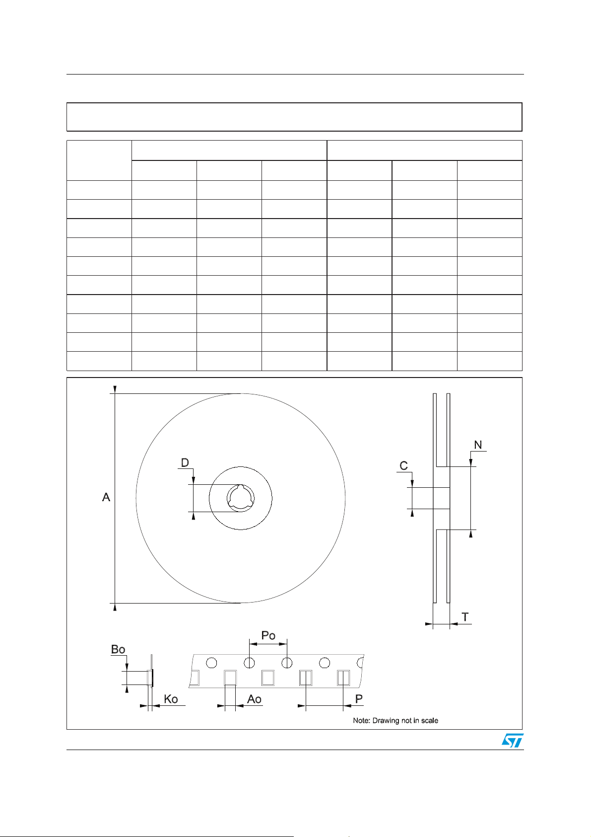
Package mechanical data STPM11, STPM12, STPM13, STPM14
Tape & reel TSSOP20 mechanical data
mm. inch.
Dim.
Min. Typ. Max. Min. Typ. Max.
A 330 12.992
C 12.8 13.2 0.504 0.519
D 20.2 0.795
N60 2.362
T 22.4 0.882
Ao 6.8 7 0.268 0.276
Bo 6.9 7.1 0.272 0.280
Ko 1.7 1.9 0.067 0.075
Po 3.9 4.1 0.153 0.161
P 11.9 12.1 0.468 0.476
44/46 Doc ID 13167 Rev 8

STPM11, STPM12, STPM13, STPM14 Revision history
12 Revision history
Table 20. Document revision history
Date Revision Changes
30-Jan-2007 1 Initial release.
06-Feb-2007 2 The Figure 11 has been changed.
20-Mar-2007 3 General description has been updated.
13-Sep-2007 4 Add Ta bl e 1 in cover page.
21-Jan-2008 5 Added Note: on page 39.
07-Apr-2009 6 Modified paragraph 7.14 on page 25.
16-Mar-2011 7 Modified Table 16 on page 30.
09-Jun-2011 8 Modified Section 7.1 on page 15.
Doc ID 13167 Rev 8 45/46

STPM11, STPM12, STPM13, STPM14
Please Read Carefully:
Information in this document is provided solely in connection with ST products. STMicroelectronics NV and its subsidiaries (“ST”) reserve the
right to make changes, corrections, modifications or improvements, to this document, and the products and services described herein at any
time, without notice.
All ST products are sold pursuant to ST’s terms and conditions of sale.
Purchasers are solely responsible for the choice, selection and use of the ST products and services described herein, and ST assumes no
liability whatsoever relating to the choice, selection or use of the ST products and services described herein.
No license, express or implied, by estoppel or otherwise, to any intellectual property rights is granted under this document. If any part of this
document refers to any third party products or services it shall not be deemed a license grant by ST for the use of such third party products
or services, or any intellectual property contained therein or considered as a warranty covering the use in any manner whatsoever of such
third party products or services or any intellectual property contained therein.
UNLESS OTHERWISE SET FORTH IN ST’S TERMS AND CONDITIONS OF SALE ST DISCLAIMS ANY EXPRESS OR IMPLIED
WARRANTY WITH RESPECT TO THE USE AND/OR SALE OF ST PRODUCTS INCLUDING WITHOUT LIMITATION IMPLIED
WARRANTIES OF MERCHANTABILITY, FITNESS FOR A PARTICULAR PURPOSE (AND THEIR EQUIVALENTS UNDER THE LAWS
OF ANY JURISDICTION), OR INFRINGEMENT OF ANY PATENT, COPYRIGHT OR OTHER INTELLECTUAL PROPERTY RIGHT.
UNLESS EXPRESSLY APPROVED IN WRITING BY AN AUTHORIZED ST REPRESENTATIVE, ST PRODUCTS ARE NOT
RECOMMENDED, AUTHORIZED OR WARRANTED FOR USE IN MILITARY, AIR CRAFT, SPACE, LIFE SAVING, OR LIFE SUSTAINING
APPLICATIONS, NOR IN PRODUCTS OR SYSTEMS WHERE FAILURE OR MALFUNCTION MAY RESULT IN PERSONAL INJURY,
DEATH, OR SEVERE PROPERTY OR ENVIRONMENTAL DAMAGE. ST PRODUCTS WHICH ARE NOT SPECIFIED AS "AUTOMOTIVE
GRADE" MAY ONLY BE USED IN AUTOMOTIVE APPLICATIONS AT USER’S OWN RISK.
Resale of ST products with provisions different from the statements and/or technical features set forth in this document shall immediately void
any warranty granted by ST for the ST product or service described herein and shall not create or extend in any manner whatsoever, any
liability of ST.
ST and the ST logo are trademarks or registered trademarks of ST in various countries.
Information in this document supersedes and replaces all information previously supplied.
The ST logo is a registered trademark of STMicroelectronics. All other names are the property of their respective owners.
© 2011 STMicroelectronics - All rights reserved
Australia - Belgium - Brazil - Canada - China - Czech Republic - Finland - France - Germany - Hong Kong - India - Israel - Italy - Japan -
STMicroelectronics group of companies
Malaysia - Malta - Morocco - Philippines - Singapore - Spain - Sweden - Switzerland - United Kingdom - United States of America
www.st.com
46/46 Doc ID 13167 Rev 8
 Loading...