

ST STPIC6C595 User Manual
Features
STPIC6C595
Power logic 8-bit shift register
■ Low R
■ 30 mJ avalanche energy
■ Eight 100 mA DMOS outputs
■ 250 mA current limit capability
■ 33 V output clamp voltage
■ Device are cascadable
■ Low power consumption
DS(on)
: 4 Ω typ
Description
This STPIC6C595 is a monolithic, mediumvoltage, low current power 8-bit shift register
designed for use in systems that require relatively
moderate load power such as LEDs. The device
contains a built-in voltage clamp on the outputs
for inductive transient protection. Power driver
applications include relays, solenoids, and other
low-current or medium-voltage loads.
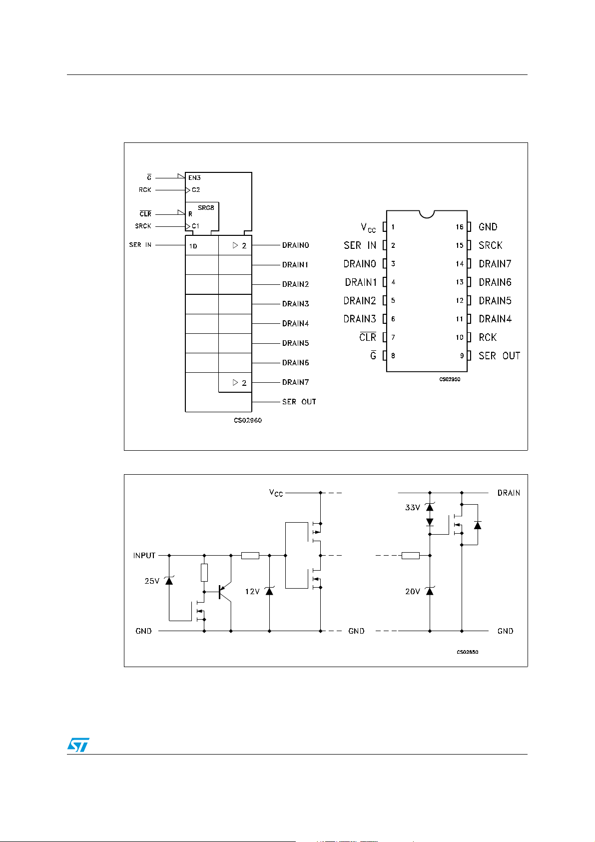
The device contains an 8-bit serial-in, parallel-out
shift register that feeds an 8-bit D-type storage
register. Data transfers through both the shift and
storage register clock (SRCK) and the register
clock (RCK
data out the serial output (SER OUT) port on the
rising edge of SRCK. The storage register
transfers data to the output buffer when shift
register clear (CLR) is high. When CLR
input shift register is cleared. When output enable
(G
) is held high, all data in the output buffer is
held low and all drain output are off. When G is
held low, data from the storage register is
transparent to the output buffer.
), respectively. The device transfers
is low, the
SO-16 TSSOP16
When data in the output buffers is low, the DMOS
transistor outputs are off. When data is high, the
DMOS transistor outputs have sink-current
capability. The SER OUT allows for cascading of
the data from the shift register to additional
devices.
Output are low-side, open-drain DMOS
transistors with output ratings of 33 V and 100 mA
continuous sink-current capability. Each output
provides a 250 mA maximum current limit at
T
= 25 °C. The current limit decreases as the
C
junction temperature increases for additional
device protection. The device also provides up to
1.5 kV of ESD protection when tested using the
human-body model and 150 V machine model.
The STPIC6C595 is characterized for operation
over the operating case temperature range of
-40 °C to 125 °C.
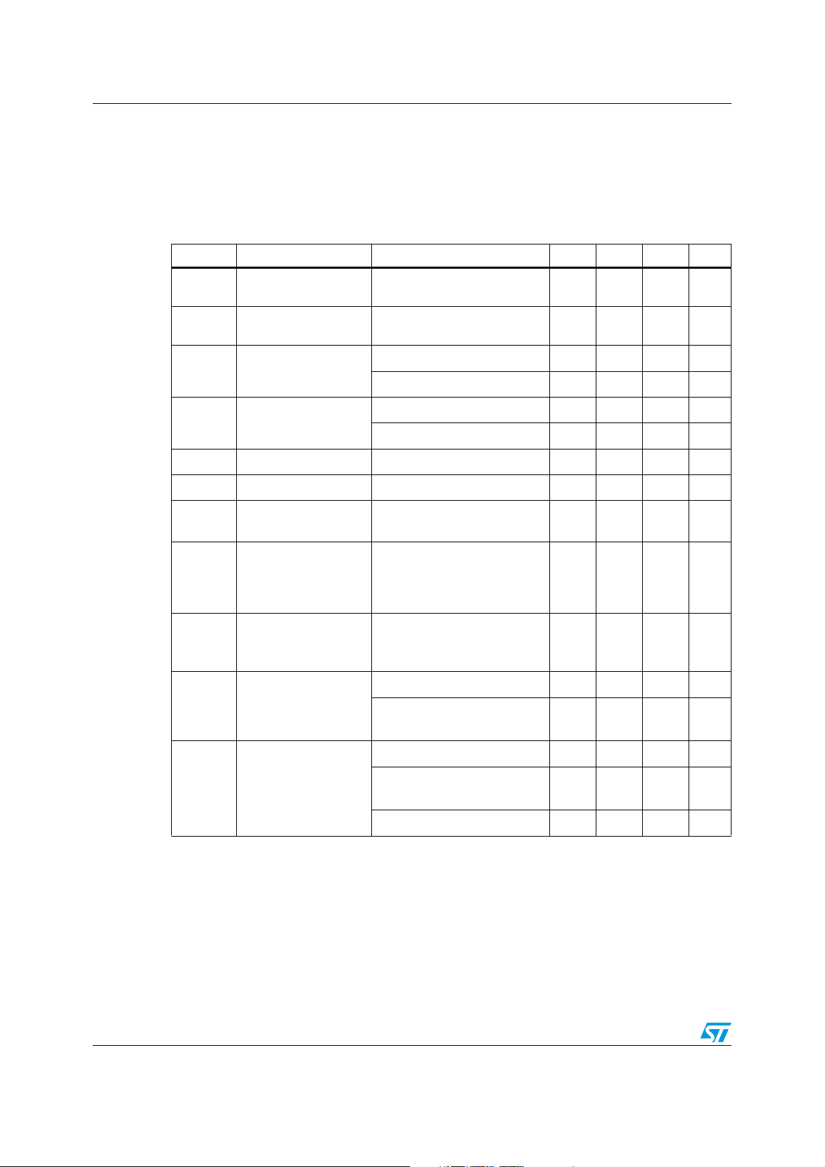
Table 1. Device summary
Order codes Package Packaging
STPIC6C595MTR SO-16 (Tape and reel) 2500 parts per reel
STPIC6C595TTR TSSOP16 (Tape and reel) 2500 parts per reel
March 2009 Rev 5 1/22
www.st.com
22

Contents STPIC6C595
Contents
1 Logic symbol and pin configuration . . . . . . . . . . . . . . . . . . . . . . . . . . . . 3
2 Maximum rating . . . . . . . . . . . . . . . . . . . . . . . . . . . . . . . . . . . . . . . . . . . . . 4
2.1 Absolute maximum ratings . . . . . . . . . . . . . . . . . . . . . . . . . . . . . . . . . . . . . 4
2.2 Thermal data . . . . . . . . . . . . . . . . . . . . . . . . . . . . . . . . . . . . . . . . . . . . . . . 5
2.3 Recommended operating conditions . . . . . . . . . . . . . . . . . . . . . . . . . . . . . 5
3 Electrical characteristics . . . . . . . . . . . . . . . . . . . . . . . . . . . . . . . . . . . . . 6
3.1 DC characteristics . . . . . . . . . . . . . . . . . . . . . . . . . . . . . . . . . . . . . . . . . . . 6
3.2 Switching characteristics . . . . . . . . . . . . . . . . . . . . . . . . . . . . . . . . . . . . . . 7
4 Logic diagram . . . . . . . . . . . . . . . . . . . . . . . . . . . . . . . . . . . . . . . . . . . . . . 8
5 Typical operating circuit . . . . . . . . . . . . . . . . . . . . . . . . . . . . . . . . . . . . . . 9
6 Typical performance and characteristics . . . . . . . . . . . . . . . . . . . . . . . 13
7 Package mechanical data . . . . . . . . . . . . . . . . . . . . . . . . . . . . . . . . . . . . 16
8 Revision history . . . . . . . . . . . . . . . . . . . . . . . . . . . . . . . . . . . . . . . . . . . 21
2/22
STPIC6C595 Logic symbol and pin configuration
1 Logic symbol and pin configuration
Figure 1. Logic symbol and pin configuration
Figure 2. Input and output equivalent circuits
3/22
Maximum rating STPIC6C595
2 Maximum rating
Stressing the device above the rating listed in the “absolute maximum ratings” table may
cause permanent damage to the device. These are stress ratings only and operation of the
device at these or any other conditions above those indicated in the operating sections of
this specification is not implied. Exposure to absolute maximum rating conditions for
extended periods may affect device reliability.
2.1 Absolute maximum ratings
Table 2. Absolute maximum ratings
Symbol Parameter Value Unit
V
V
I
I
Logic supply voltage (See Note 1)7V
CC
V
Logic input voltage range -0.3 to 7 V
I
Power DMOS drain to source voltage (See Note 2)33V
DS
Continuous source to drain diode anode current 250 mA
DS
Pulsed source to drain diode anode current
DS
(See Note 3)
Pulsed drain current, each output, all output ON
I
D
I
D
I
D
= 25 °C)
(T
C
Continuous current, each output, all output ON
= 25 °C)
(T
C
Peak drain current single output
(TC = 25 °C) (See Note 3)
500 mA
250 mA
100 mA
250 mA
E
I
T
Single pulse avalanche energy
AS
(See Figure 11 and Figure 12)
Avalanche current (See Note 4 and Figure 17)200mA
AS
P
Continuous total dissipation (TC ≤ 25 °C)
d
P
Continuous total dissipation (TC = 125 °C)
d
T
Operating virtual junction temperature range -40 to +150 °C
J
T
Operating case temperature range -40 to +125 °C
C
Storage temperature range -65 to +150 °C
stg
Lead temperature 1.6 mm (1/16 inch) from case for 10
T
L
seconds
4/22
30 mJ
1087 mW
217 mW
260 °C
STPIC6C595 Maximum rating
2.2 Thermal data
Table 3. Thermal data
Symbol Parameter Value Unit
R
th(JA)
Thermal resistance junction-ambient 115 °C/W
2.3 Recommended operating conditions
Table 4. Recommended operating conditions
Symbol Parameter Min Typ Max Unit
V
CC
V
V
I
DP
t
su
t
hL
Logic supply voltage 4.5 5.5 V
High level input voltage
IH
Low level input voltage 0
IL
0.85V
CC
Pulse drain output current
(TC = 25 °C, V
= 5 V, all outputs ON)
CC
(see Note 3, Note 5 and Figure 15)
Set-up time, SER IN high before SRCK ↑
(see Figure 4 and Figure 8)
Hold time, SER IN high before G ↑
(see Figure 4, Figure 7, Figure 8)
1.6 3.0 5.7 ns
2.8 4.0 9.6 ns
V
CC
0.15V
CC
250 mA
V
V
t
W
T
Pulse duration (see Figure 8)40ns
Operating case temperature -40 125 °C
C
5/22
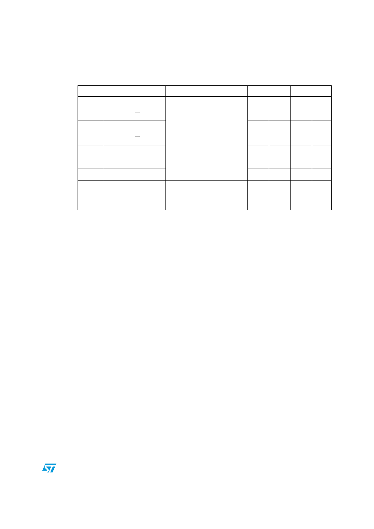
Electrical characteristics STPIC6C595
3 Electrical characteristics
3.1 DC characteristics
Table 5. DC characteristics (V
Symbol Parameter Test conditions Min Typ Max Unit
V
(BR)DSX
V
V
V
I
I
I
CC
I
CC(FRQ)
I
I
DSX
R
DS(on)
Drain-to-source
breakdown voltage
Source-to-drain diode
SD
forward voltage
High level output
OH
voltage SER OUT
Low level output
OL
voltage SER OUT
High level input current
IH
Low level input current
IL
Logic supply current
Logic supply current at
frequency
Nominal current
N
Off-state drain current
Static drain source on
state resistance
(See Note 5, Note 6
and Figure 14,
Figure 16)
= 5 V, TC = 25 °C, unless otherwise specified.)
CC
ID = 1 mA
IF = 100 mA
= -20 μA, VCC = 4.5 V
I
OH
I
= -4 mA, VCC = 4.5 V
OH
IOH = 20 μA, VCC = 4.5 V
I
= 4 mA, VCC = 4.5 V
OH
= 5.5 V, VI = V
V
CC
= 5.5 V, VI = 0
V
CC
CC
VCC = 5.5 V, all outputs OFF or
ON
= 5 MHz, CL = 30 pF
f
SRCK
All outputs OFF
(See Figure 6, Figure 18 and
33 37 V
0.85 1.2 V
4.4 4.49 V
44.2 V
0.005 0.1 V
0.3 0.5 V
20 200 μA
0.2 2 mA
Figure 19)
V
= 0.5 VIN = I
DS(on)
TC = 85 °C
D
90 mA
(See Note 5, Note 6, Note 7)
= 30 V, VCC = 5.5 V
V
DS
V
= 30 V, VCC =5.5 V or 0 V
DS
= 125 °C
T
C
= 50 mA, VCC = 4.5 V
I
D
I
= 50 mA, VCC = 4.5 V
D
= 125 °C
T
C
I
= 100 mA, VCC = 4.5 V
D
0.3 5 μA
0.6 8 μA
4.5 6 Ω
6.5 9 Ω
4.5 6 Ω
1 μA
-1 μA
6/22
STPIC6C595 Electrical characteristics
3.2 Switching characteristics
Table 6. Switching characteristics (V
Symbol Parameter Test conditions Min Typ Max Unit
Propagation delay
t
time, high to low level
PHL
output from G
= 5 V, TC = 25 °C, unless otherwise specified.)
CC
80 ns
t
PLH
t
Propagation delay
time, low to high level
output from G
t
Rise time, drain output 60 ns
r
t
Fall time, drain output 50 ns
f
propagation delay time 20 ns
pd
Reverse recovery
t
a
current rise time
t
Reverse recovery time 115 ns
rr
CL = 30 pF, ID = 75 mA
(See Figure 4, Figure 5,
Figure 6, Figure 7, Figure 20)
= 100 mA, di/dt = 10 A/μs
I
F
(See Figure 5, Figure 6, and
Figure 9, Figure 10 )
Note: 1 All voltage value are with respect to GND
2 Each power DMOS source is internally connected to GND
3 Pulse duration
≤
100 μs and duty cycle ≤ 2 %
4 Drain supply voltage = 15 V, starting junction temperature (T
I
= 200 mA (see Fig. 11 and 12)
AS
5 Technique should limit T
- TC to 10 °C maximum
J
6 These parameters are measured with voltage sensing contacts separate from the current-
carrying contacts.
7 Nominal current is defined for a consistent comparison between devices from different
sources. It is the current that produces a voltage drop of 0.5 V at T
130 ns
39 ns
) = 25 °C. L = 1.5 H and
JS
= 85 °C.
C
7/22
 Loading...