

查询STF9NK80Z供应商
N-CHANNEL 800V -0.9Ω - 7.5A TO-220/TO -2 20F P
STP9NK80Z
STF9NK80Z
Zener-Protected SuperMESH™MOSFET
Table 1: Ge neral Features
TYPE V
STP9NK80Z
STF9NK80Z
■ TYPICAL R
■ EXTREMELY HIGH dv/d t C APABILITY
■ IMPROVED ESD CAPABILITY
■ 100% AVALANCHE RATED
■ GATE CHARGE MINIMIZED
■ VERY LOW INTRINSIC CAPACITANCES
■ VERY GOOD MANUFACTURING
DSS
800 V
800 V
(on) = 0.9Ω
DS
R
DS(on)ID
<1.2 Ω
<1.2 Ω
7.5 A
7.5 A
Pw
150 W
35 W
REPEATIBILITY
DESCRIPTION
The SuperMESH™ s eries is obtained through an
extreme optimization of ST’s well established
strip-based PowerMESH™ layout. In addition to
pushing on-resistance significantly down , special
care is taken to ensure a very good dv/dt capability
for the most demanding applications. Such series
complements ST full range of high voltage MOS FET s including revolutionary MDmesh™ products.
APPLICATIONS
■ HIGH CURRENT, HIGH SPEED SWITCHING
■ IDEAL FOR OFF-L INE POWER SUPPL IES
■ SMPS
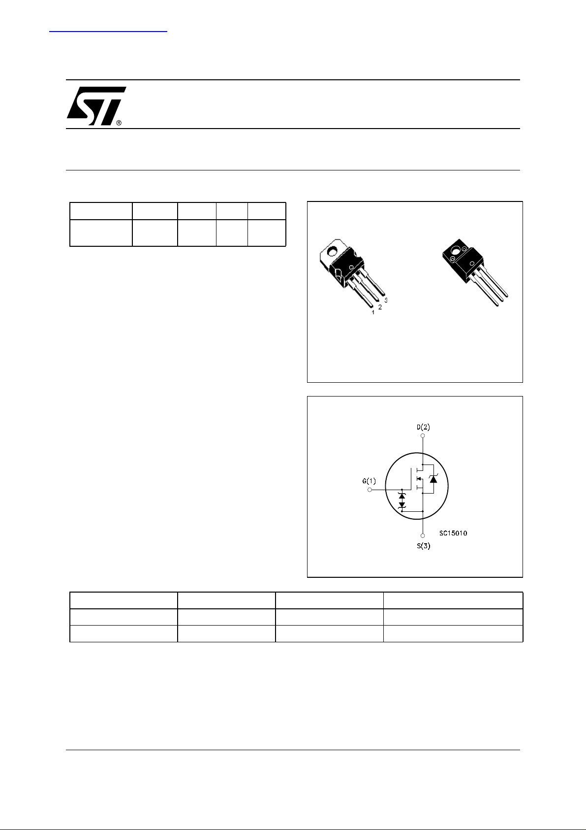
Figure 1: Package
TO-220 TO-220FP
Figure 2: Internal Schematic Diagram
3
2
1
Table 2: Order Codes
SALES TYPE MARKING PACKAGE PACKAGING
STP9NK80Z P9NK80Z TO-220 TUBE
STF9NK80Z F9NK80Z TO-220FP TUBE
Rev. 1
1/11May 2005
STP9NK80Z - STF9NK80Z
Table 3: Absolute Maximum ratings
Symbol Parameter Value Unit
TO-220 TO-220FP
V
DS
V
DGR
V
GS
I
D
I
D
I
DM
P
TOT
V
ESD(G-S)
dv/dt (1) Peak Diode Recovery voltage slope 4.5 V/ns
V
ISO
T
j
T
stg
() Pulse wi dt h l i m i ted by safe operating area
≤7.5A, di/dt ≤200A/µs, VDD = 80% V
(1) I
SD
(*) Limited only by maximum temperature allowed
Drain-source Voltage (VGS = 0)
Drain-gate Voltage (RGS = 20 kΩ)
800 V
800 V
Gate- source Voltage ± 30 V
Drain Current (continuous) at TC = 25°C
Drain Current (continuous) at TC = 100°C
()
Drain Current (pulsed) 30 30 (*) A
Total Dissipation at TC = 25°C
7.5 7.5 (*) A
4.7 4.7 (*) A
150 35 W
Derating Factor 1.20 0.28 W/°C
Gate source ESD(HBM-C=100pF, R=1.5KΩ) 4000 V
Insulation Withstand Voltage (DC) - 2500 V
Operating Junction Temperature
Storage Temperature
(BR)DSS
-55 to 150
-55 to 150
°C
°C
Table 4: Thermal Data
TO-220 TO-220FP
Rthj-case Thermal Resistance Junction-case Max 0.83 3.6 °C/W
Rthj-amb Thermal Resistance Junction-ambient Max 62.5 °C/W
T
l
Maximum Lead Temperature For Soldering
350 °C
Purpose
Table 5: Avalanche Characteristics
Symbol Parameter Max Value Unit
I
AR
E
AS
Avalanche Current, Repetitive or Not-Repetitive
(pulse width limited by T
max)
j
Single Pulse Avalanche Energy
(starting T
= 25 °C, ID = IAR, VDD = 50 V)
j
7.5 A
350 mJ
Table 6: Gate-Source Zener Diode
Symbol Parameter Test Conditions Min. Typ. Max. Unit
BV
GSO
Gate-Source
Igs=± 1mA (Open Drain) 30 V
Breakdown Voltage
PROTECTION FEATURES OF GATE-TO-SOURCE ZENER DIODES
The built-in back-to-back Zener diodes have specifically been designed to enhance not only the device’s
ESD capability, but also to make them safely absorb possible voltage transients that may occasionally be
applied from gate to source. In this respect the Zener voltage is appropriate to achieve an efficient and
cost-effective intervention to protect the device’s integrity. These integrated Ze ner diodes thus avoid the
usage of external components.
2/11
STP9NK80Z - STF9NK80Z
ELECTRICAL CHARACTERISTICS (T
=25°C UNLESS OTHERWISE SPECIFIED)
CASE
Table 7: On/Off
Symbol Parameter Test Conditions Min. Typ. Max. Unit
V
(BR)DSS
Drain-source
ID = 1 mA, VGS = 0 800 V
Breakdown Voltage
I
DSS
I
GSS
V
GS(th)
R
DS(on)
Zero Gate Voltage
Drain Current (V
GS
= 0)
Gate-body Leaka ge
Current (V
DS
= 0)
Gate Threshold Voltage
Static Drain-source On
V
= Max Rating
DS
V
= Max Rating, TC = 125 °C
DS
V
= ± 20V ±10 µA
GS
V
= VGS, ID = 100µA
DS
33.754.5V
1
50
VGS = 10V, ID = 3.75 A 0.9 1.2 Ω
Resistance
Table 8: DYNAMIC
Symbol Parameter Test Conditions Min. Typ. Max. Unit
(1) Forward Transconductance VDS = 15 V, ID= 3.75 A 7.5 S
g
fs
C
oss eq.
C
C
C
t
d(on)
t
d(off)
iss
oss
rss
t
r
t
f
Input Capacitance
Output Capacitance
Reverse Transfer
Capacitance
(3) Equivalent Outpu t
Capacitance
Turn-on Delay Time
Rise Time
Turn-off Delay Time
Fall Time
= 25V, f = 1 MHz, VGS = 0 1900
V
DS
180
38
VGS = 0V, VDS = 0V to 640V 75 pF
= 400 V, ID = 3.75 A
V
DD
R
=4.7Ω VGS = 10 V
G
(see Figure 19)
26
19
58
18
µA
µA
pF
pF
pF
ns
ns
ns
ns
= 640 V, ID = 7.5A,
t
r(Voff)
t
t
Q
Q
Q
Off-voltage Rise Time
f
c
g
gs
gd
Fall Time
Cross-over Time
Total Gate Charge
Gate-Source Charge
Gate-Drain Charge
V
DD
RG=4.7Ω, V
GS
(see Figure 20)
= 640V, ID = 7.5 A,
V
DD
VGS = 10V
(see Figure 22)
= 10V
12
10
24
60
12
35
84
Table 9: Source Drain Diode
Symbol Parameter Test Conditions Min. Typ. Max. Unit
I
SD
I
(2)
SDM
(1)
V
SD
t
rr
Q
rr
I
RRM
t
rr
Q
rr
I
RRM
Note: 1. Pulsed: P ul se duration = 300 µs, duty cyc l e 1.5 %.
2. Pulse wi dt h l i m ited by safe operating area.
3. C
Source-drain Current
Source-drain Current (pulsed)
Forward On Voltage
Reverse Recovery Time
Reverse Recovery Charge
Reverse Recovery Current
Reverse Recovery Time
Reverse Recovery Charge
Reverse Recovery Current
is defined as a constant equivalent capacitance giving the same charging time as C
oss eq.
.
V
DSS
ISD = 7.5 A, VGS = 0
I
SD
VDD = 35V, Tj = 25°C
(see Figure 20)
I
SD
V
DD
(see Figure 20)
= 7.5 A, di/dt = 100A/µs
= 7.5 A, di/dt = 100A/µs
= 35V, Tj = 150°C
530
4.5
17
690
6.4
17
when VDS increases from 0 to 80%
oss
7.5
30
1.6 V
ns
ns
ns
nC
nC
nC
A
A
ns
µC
A
ns
µC
A
3/11
STP9NK80Z - STF9NK80Z
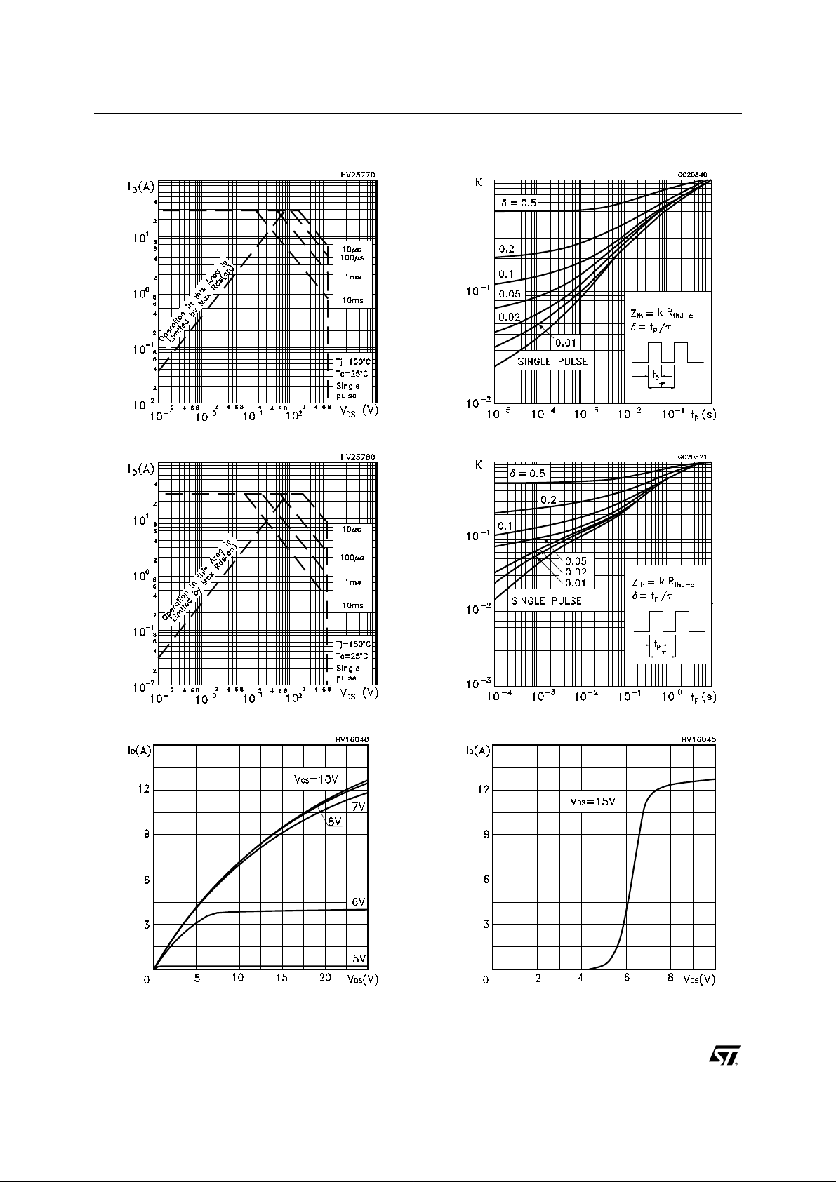
Figure 3: Safe Operating Area for TO-220
Figure 4: Safe Operating Area for TO-220FP
Figure 6: Thermal Impedan ce for TO -2 20
Figure 7: Thermal Impedan ce for TO -2 20FP
Figure 5: Output Characteristics
4/11
Figure 8: Transfer Characteristics
STP9NK80Z - STF9NK80Z
Figure 9: Transconductance
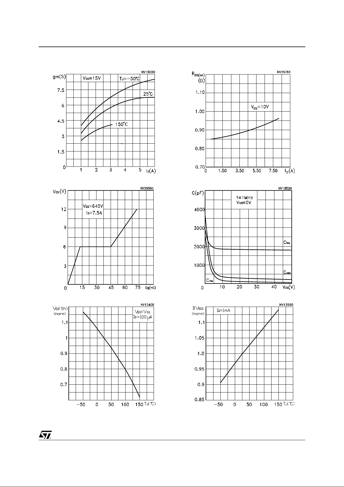
Figure 10: Gate Charge vs Gate-source Voltage
Figure 12: Static Drain-source On Resistance
Figure 13: Capacitance Variations
Figure 11: Normalized Gate Thereshold Voltage vs Temperature
Figure 14: Normalized BVDSS vs Temperature
5/11

STP9NK80Z - STF9NK80Z
Figure 15: Norm alized O n Resis tance vs T emperatureS
Figure 16: Avalanche Energy vs Temp eratur e
Figure 17: S ource-Drain Diode Forw ard Characteristics
6/11

STP9NK80Z - STF9NK80Z
Figure 18: Unclamped Inductive Load Test Circuit
Figure 19: Switching Times Test Circuit For
Resistive Load
Figure 21: Unclamped Inductive Wafeform
Figure 22: Gate Charge Test Circuit
Figure 20: Test Circuit For Inductive Load
Switching and Diode Recovery Times
7/11

STP9NK80Z - STF9NK80Z
TO-220 MECHANICAL DATA
DIM.
A 4.40 4.60 0.173 0.181
b 0.61 0.88 0.024 0.034
b1 1.15 1.70 0.045 0.066
c 0.49 0.70 0.019 0.027
D 15.25 15.75 0.60 0.620
E 10 10.40 0.393 0.409
e 2.40 2.70 0.094 0.106
e1 4.95 5.15 0.194 0.202
F 1.23 1.32 0.048 0.052
H1 6.20 6.60 0.244 0.256
J1 2.40 2.72 0.094 0.107
L 13 14 0.511 0.551
L1 3.50 3.93 0.137 0.154
L20 16.40 0.645
L30 28.90 1.137
øP 3.75 3.85 0.147 0.151
Q 2.65 2.95 0.104 0.116
MIN. TYP MAX. MIN. TYP. MAX.
mm. inch
8/11

TO-220FP MECHANICAL DATA
STP9NK80Z - STF9NK80Z
DIM.
A 4.4 4.6 0.173 0.181
B 2.5 2.7 0.098 0.106
D 2.5 2.75 0.098 0.108
E 0.45 0.7 0.017 0.027
F 0.75 1 0.030 0.039
F1 1.15 1.7 0.045 0.067
F2 1.15 1.7 0.045 0.067
G 4.95 5.2 0.195 0.204
G1 2.4 2.7 0.094 0.106
H 10 10.4 0.393 0.409
L2 16 0.630
L3 28.6 30.6 1.126 1.204
L4 9.8 10.6 .0385 0.417
L5 2.9 3.6 0.114 0.141
L6 15.9 16.4 0.626 0.645
L7 9 9.3 0.354 0.366
Ø 3 3.2 0.118 0.126
MIN. TYP MAX. MIN. TYP. MAX.
mm. inch
E
A
D
B
L3
L6
L7
F1
F
G1
H
F2
123
L2
L5
L4
G
9/11
STP9NK80Z - STF9NK80Z
Table 10: Revision History
Date R evisio n Descrip tion of Change s
18-May-2005 1 First Release.
10/11

STP9NK80Z - STF9NK80Z
Information furnished is believed to be accurate and reliable. However, STMicroelectronics assumes no responsibility for the consequences
of use of such information nor for any infringement of patents or other rights of third parties which may result from its use. No license is g ranted
by implic ati o n or ot h er wis e und er an y pat ent or pa te nt r igh ts of STMi cr oe l ect ro ni cs . Sp ec if i cat i on s ment i o ned i n th is p ub li c ati on ar e s ubj ec t
to change without notice. This public ation supersedes and replaces all information previously supplie d. STMicroelectronics pro ducts are not
authorized for use as critical components in life support devices or systems without express written approval of STMicroelectronics.
The ST logo is a registered trademark of STMicroelectronics
All other names are the property of their respective owners
© 2005 STMicroelectronics - All Rights Reserved
STMicroelectronics group of companies
Australia - Belgium - Brazil - Canada - China - Czech Republic - Finland - France - Germany - Hong Kong - India - Israel - Italy - Japan -
Malaysia - Malta - Morocco - Singapore - Spain - Sweden - Switzerland - United Kingdom - United States of America
11/11
 Loading...