

STB80NF55-06 STB80NF55-06-1
1
3
3
1
3
3
STP80NF55-06 STP80NF55-06FP
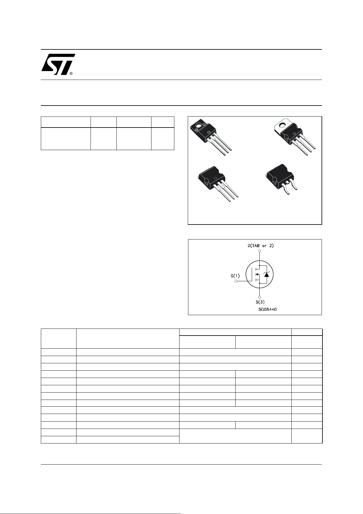
N-CHANNEL 55V - 0.005 Ω - 80A TO-220/TO-220FP/I
STripFET™ II POWER MOSFET
TYPE
STB80NF55-06/-1
STP80NF55-06
STP80NF55-06FP
■ TYPICAL R
■ EXCEPTIONAL dv/dt CAPABILITY
■ 100% AVALANCHE TESTED
■ APPLICATION ORIENTED
DS
V
DSS
55 V
55 V
55 V
(on) = 0.005 Ω
CHARACTERIZATION
■ SURFACE-MOUNTING D
POWER PACKAGE IN TU BE (NO SUFFIX) OR
IN TAPE & REEL (SUFFIX “T4”)
DESCRIPTION
This Power MOSFET is the latest development of
STMicroelectronis unique "Single Feature Size™"
strip-based process. The resulting transistor
shows extremely high p acking density for low onresistance, rugged ava lanche characteristics and
less critical alignment steps therefore a remarkable manufacturing reproducibility.
R
DS(on)
<0.0065
Ω
<0.0065 Ω
<0.0065 Ω
2
PAK (TO-263)
I
D
80 A
80 A
60 A
TO-220FP
2
2
PAK
1
²
I
TO-262
(Suffix “-1”)
INTERNAL SCHEMATIC DIAGRAM
²
PAK/D²PAK
TO-220
1
D²PAK
TO-263
(Suffix “T4”)
2
APPLICATIONS
■ HIGH-EFFICIENCY DC-DC CONVERTERS
■ UPS AND MOTOR CONTROL
■ DC-DC CONVERTERS
■ AUTOMOTIVE ENVIRONMENT
ABSOLUTE MAXIMUM RATINGS
Symbol Parameter Value Unit
STB80NF55-06/-1
STP80NF55-06
I
V
DM
V
DGR
V
I
I
P
DS
GS
D
D
(•)
tot
Drain-source Voltage (VGS = 0)
Drain-gate Voltage (RGS = 20 kΩ)
Gate- source Voltage ± 20 V
Drain Current (conti nuo us ) at TC = 25°C
Drain Current (conti nuo us ) at TC = 100°C
80 60 A
80 42 A
Drain Current (pulse d) 320 240 A
Total Dissipation at TC = 25°C
300 45 W
Derating Factor 2 0.30 W/°C
(1)
dv/dt
E
AS
V
ISO
T
stg
T
j
(•) Pulse width limited by safe operating area. (1) I
NEW DATASHEET ACCORDING TO PCN DSG/CT/2C13 MARKING: P80NF55-06 @ B80NF55-06 @ P80NF55-06 @
Peak Diode Recove ry vo ltag e slo pe 7 V/ns
(2)
Single Pulse Avalanche Energy 1.3 J
Insulation Withstand Voltage (DC) ------ 2500 V
Storage Temperature
Operating Junction Temperature
≤80A, di/dt ≤400A/µs, VDD ≤ V
SD
(2) Starting Tj = 25 oC, ID = 40A, VDD= 35V
STP80NF55-06FP
55 V
55 V
-55 to 175 °C
, Tj ≤ T
(BR)DSS
JMAX
1/12February 2004
STB80NF55-06/-1 STP80NF55-06 STP80NF55-06FP
THERMAL DATA
D2PAK/I2PAK/
TO-220
Rthj-case Thermal Resistance Junction-case Max 0.5 3.33 °C/W
Rthj-amb
T
Thermal Resistance Junction-ambient
Maximum Lead Temperature For Soldering Purpose
l
Max 62.5
TO-220FP
300
°C/W
°C
ELECTRICAL CHARACTERISTICS (T
= 25 °C unless otherwise specified)
case
OFF
Symbol Parameter Test Conditions Min. Typ. Max. Unit
I
= 250 µA, VGS = 0
D
V
= Max Rating
DS
= Max Rating TC = 125°C
V
DS
= ± 20 V
V
GS
55 V
1
10
±100 nA
ON
V
(BR)DSS
I
DSS
I
GSS
(*)
Drain-source
Breakdown Voltage
Zero Gate Voltage
Drain Current (V
GS
Gate-body Leakage
Current (V
DS
= 0)
= 0)
Symbol Parameter Test Conditions Min. Typ. Max. Unit
V
GS(th)
R
DS(on)
Gate Threshold Voltage
Static Drain-source On
V
= VGS ID = 250 µA
DS
V
= 10 V ID = 40 A
GS
234V
0.005 0.0065
Resistance
DYNAMIC
Symbol Parameter Test Conditions Min. Typ. Max. Unit
(*)
g
fs
C
iss
C
oss
C
rss
Forward Transconductance
Input Capacitance
Output Capacitance
Reverse Transfer
Capacitance
V
= 15 V ID=40 A
DS
V
= 25V, f = 1 MHz, VGS = 0
DS
150 S
4400
1020
350
µA
µA
Ω
pF
pF
pF
2/12
STB80NF55-06/-1 STP80NF55-06 STP80NF55-06FP
ELECTRICAL CHARACTERISTICS (continued)
SWITCHING ON
Symbol Parameter Test Conditions Min. Typ. Max. Unit
V
t
d(on)
Q
Q
Q
t
r
g
gs
gd
Turn-on Delay Time
Rise Time
Total Ga te Char ge
Gate-Source Charg e
Gate-Drain Charge
SWITCHING OFF
Symbol Parameter Test Conditions Min. Typ. Max. Unit
t
d(off)
t
f
Turn-off Delay Time
Fall Time
SOURCE DRAIN DIODE
Symbol Parameter Test Conditions Min. Typ. Max. Unit
I
SD
I
SDM
V
SD
t
rr
Q
rr
I
RRM
(*)
Pulsed: Pulse duration = 300 µs, duty cycle 1.5 %.
(
•)Pulse width limited by safe operating area.
Source-drain Curre nt
(•)
Source-drain Curre nt (pu lse d)
(*)
Forward On Voltage
Reverse Recovery Time
Reverse Recovery Charge
Reverse Recovery Current
= 27 V ID = 40 A
DD
=4.7 Ω VGS = 10 V
R
G
(Resistive Load, Figu re 3)
V
= 44 V ID= 80 A VGS= 10V
DD
V
= 27 V ID = 40 A
DD
=4.7Ω, V
R
G
GS
= 10 V
(Resistive Load, Figu re 3)
I
= 80 A VGS = 0
SD
I
= 80 A di/dt = 100A/µs
SD
= 35 V Tj = 150°C
V
DD
(see test circuit, Figure 5)
27
155
142
29
60.5
125
65
100
0.32
6.5
193 nC
80
320
1.5 V
ns
ns
nC
nC
ns
ns
A
A
ns
µC
A
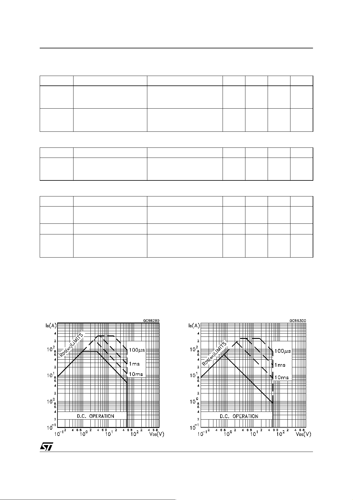
Safe Operating Area for TO-220FPSafe Operating Area for TO-220
3/12

STB80NF55-06/-1 STP80NF55-06 STP80NF55-06FP
Thermal Impedance Thermal Impedance for TO-220FP
Output Characteristics Transfer Characteristics
Transconductance Static Drain-source On Resistance
4/12
 Loading...