

ST STP7NK80Z, STP7NK80ZFP, STB7NK80Z, STB7NK80Z-1 User Manual
现货库存、技术资料、百科信息、热点资讯,精彩尽在鼎好!
STP7NK80Z - STP7NK80ZFP
STB7NK80Z - STB7NK80Z-1
N-CHANNEL800V-1.5Ω - 5.2A TO-220/TO-220FP/I2PAK/D2PAK
Zener-Protected SuperMESH™Power MOSFET
TYPE V
STP7NK80Z
STP7NK80ZFP
STB7NK80Z
STB7NK80Z-1
■ TYPICAL R
■ EXTREMELY HIGH dv/dt CAPABILITY
■ 100% AVALANCHE TESTED
■ GAT E CHARGE MINIMIZED
■ VERY LOW INTRINSIC CAPACITANCES
■ VER Y GO OD MANUFACTURING
800 V
800 V
800 V
800 V
(on) = 1.5 Ω
DS
DSS
R
DS(on)
< 1.8 Ω
< 1.8 Ω
< 1.8 Ω
< 1.8 Ω
I
D
5.2 A
5.2 A
5.2 A
5.2 A
Pw
125 W
30 W
125 W
125 W
REPEATIBILITY
DESCRIPTION
The SuperMESH™ series is obtained through an
extreme optimization of ST’s well established s tri pbased PowerMESH™ layout. In addition to pushing
on-resistance significantly down, special careis taken t o ensure a very good dv/dt capability for the
most demanding applicat ions. Such series complements ST full range of high voltage MOSFETs including revolutionary MDm es h™ products.
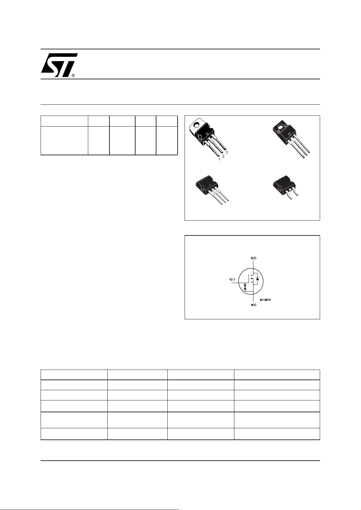
TO-220
3
2
1
TO-220FP
D2PAK
I2PAK
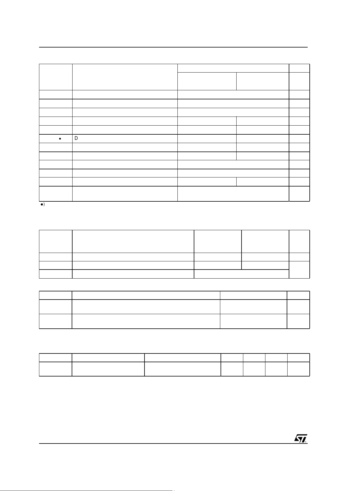
INTERNAL SCHEMATIC DIAGRAM
3
2
1
3
1
APPLICATIONS
■ HIGH CURRENT,HIGH SPEED SWITCHING
■ SMPS FOR INDUSTRIAL APPLICATION.
■ LIGHT ING (PREHE ATING)
ORDERING INFORMATION
SALES TYPE MARKING PACKAGE PACKAGING
STP7NK80Z P7NK80Z TO-220 TUBE
STP7NK80ZFP P7NK80ZFP TO-220FP TUBE
STB7NK80ZT4 B7NK80Z
STB7NK80Z B7NK80Z
STB7NK80Z-1 B7NK80Z
2
PAK
D
2
PAK
D
2
PAK
I
(ONLY UNDER REQUEST)
TAPE & REEL
TUBE
TUBE
1/13August 2002
STP7NK80Z - STP7NK80ZFP - STB7NK80Z - STB7NK80Z-1
ABSOLUTE MAXIMUM RATINGS
Symbol Parameter Value Unit
STP7NK80Z
STB7NK80Z
STB7NK80Z-1
I
V
DM
P
V
DGR
V
I
I
TOT
DS
GS
D
D
Drain-source Voltage (VGS=0)
Drain-gate Voltage (RGS=20kΩ)
800 V
800 V
Gate- source Voltage ± 30 V
Drain Current (continuous) at TC= 25°C
Drain Current (continuous) at TC= 100°C
()
Drain Current (pulsed) 20.8 20.8 (*) A
Total Dissipation at TC= 25°C
5.2 5.2 (*) A
3.3 3.3 (*) A
125 30 W
Derating Factor 1 0.24 W/°C
V
ESD(G-S)
Gate source ESD(HBM-C=100pF, R=1.5KΩ) 4000 V
dv/dt (1) Peak Diode Recovery voltage slope 4.5 V/ns
V
ISO
T
j
T
stg
() Pulse width limited by safe operating area
(1) I
≤5.2A, di/dt ≤200A/µs, VDD≤ V
SD
(*) Limited only by maximum temperature allowed
Insulation Withstand Voltage (DC) - 2500 V
Operating Junction Temperature
Storage Temperature
(BR)DSS,Tj≤TJMAX.
-55 to 150
-55 to 150
STP7NK80ZFP
°C
°C
THERMAL DATA
TO-220
D
2
I
2
PAK
PAK
TO-220FP
Rthj-case Thermal Resistance Junction-case Max 1 4.2 °C/W
Rthj-amb Thermal Resistance Junction-ambient Max 62.5 50 °C/W
T
l
Maximum Lead Temperature For Soldering Purpose
300 °C
AVALANCHE CHARACTERISTICS
Symbol Parameter Max Value Unit
I
AR
E
AS
Avalanche Current, Repetitive or Not-Repetitive
(pulse width limited by T
max)
j
Single Pulse Avalanche Energy
(starting T
= 25 °C, ID=IAR,VDD=50V)
j
5.2 A
210 mJ
GATE-SOURCE ZENER DIODE
Symbol Parameter Test Conditions Min. Typ. Max. Unit
BV
GSO
Gate-Source Breakdown
Voltage
Igs=± 1mA (Open Drain) 30 V
PROTECTION FEATURES OF GATE-TO-SOURCE ZENER DIODES
The built-in back-to-back Zener diodes havespecifically been designed to enhance not only the dev ice’s
ESD c apability, but also to make them sa fely absorb pos sible voltage transients that may occasionally be
applied from gate to source. In this respect the Zener voltage is appropriate to achieve an efficient and
cost-effective intervention to protect the device’s integrity. These integrated Zener d iodes thus avoid t he
usage of external components.
2/13
STP7NK80Z - STP7NK 80Z FP - STB7NK80Z - STB7NK80Z-1
ELECTRICAL CHARACTERISTICS (TCASE =25°C UNLESS OT HERWISE SPECIFIED)
ON/OFF
Symbol Parameter Test Conditions Min. Typ. Max. Unit
V
(BR)DSS
Drain-source
Breakdown Voltage
I
DSS
I
GSS
V
GS(th)
R
DS(on)
Zero Gate Voltage
Drain Current (V
GS
=0)
Gate-body Leakage
Current (V
DS
=0)
Gate Threshold Voltage
Static Drain-source On
Resistance
DYNAMIC
Symbol Parameter Test Conditions Min. Typ. Max. Unit
(1) Forward Transconductance VDS=15V,ID= 2.6 A 5 S
g
fs
Input Capacitance
Output Capacitance
Reverse Transfer
Capacitance
(3) Equivalent Output
C
oss eq.
C
iss
C
oss
C
rss
Capacitance
SWITCHING ON
Symbol Parameter Test Conditions Min. Typ. Max. Unit
t
d(on)
Q
Q
Q
t
r
g
gs
gd
Turn-on Delay Time
Rise Time
Total Gate Charge
Gate-Source Charge
Gate-Drain Charge
ID=1mA,VGS= 0 800 V
V
= Max Rating
DS
VDS= Max Rating, TC= 125 °C
V
= ± 20V ±10 µA
GS
V
DS=VGS,ID
= 100µA
3 3.75 4.5 V
1
50
VGS=10V,ID= 2.6 A 1.5 1.8 Ω
=25V,f=1MHz,VGS=0 1138
V
DS
122
25
VGS=0V,VDS= 0V to 640V 50 pF
VDD=400V,ID= 2.6 A
RG= 4.7Ω VGS=10V
20
12
(Resistive Load see, Figure 3)
=640V,ID= 5.2 A,
V
DD
V
=10V
GS
40
7
56 nC
21
µA
µA
pF
pF
pF
ns
ns
nC
nC
SWITCHING OFF
Symbol Parameter Test Conditions Min. Typ. Max. Unit
t
d(off)
Turn-off Delay Time
t
f
Fall Time
VDD= 400 V, ID= 2.6 A
R
=4.7ΩVGS=10V
G
45
22
(Resistive Load see, Figure 3)
t
r(Voff)
t
t
= 640V, ID= 5.2 A,
Off-voltage Rise Time
f
c
Fall Time
Cross-over Time
V
DD
RG=4.7Ω, VGS= 10V
(Inductive Load see, Figure 5)
12
10
20
SOURCE DRAIN DIODE
Symbol Parameter Test Conditions Min. Typ. Max. Unit
I
SD
I
SDM
VSD(1)
t
rr
Q
rr
I
RRM
Note: 1. Pulsed: Pulse duration = 300 µs, duty cycle 1.5 %.
2. Pulse width limited by safe operating area.
3. C
Source-drain Current
(2)
Source-drain Current (pulsed)
Forward On Voltage
Reverse Recovery Time
Reverse Recovery Charge
Reverse Recovery Current
is defined as a constant equivalent capacitance giving the same charging time as C
oss eq.
.
V
DSS
ISD= 5.2 A, VGS=0
I
SD
VDD=50V,Tj= 150°C
(see test circuit, Figure 5)
= 5.2 A, di/dt = 100A/µs
530
3.31
12.5
when VDSincreases from 0 to 80%
oss
5.2
20.8
1.6 V
ns
ns
ns
ns
ns
A
A
ns
µC
A
3/13
STP7NK80Z - STP7NK80ZF P - STB7NK80Z - STB 7NK80Z -1
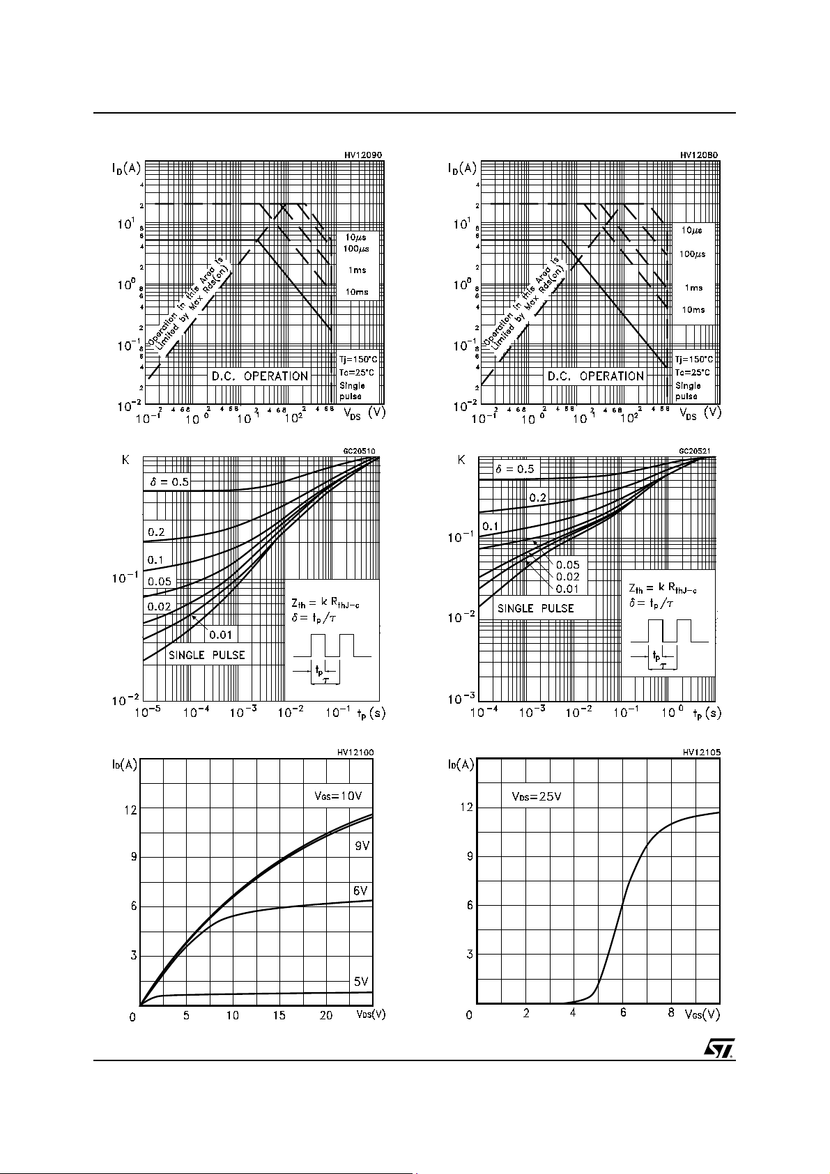
Safe Operating Area For TO-220/D2PAK/I2PAK
Thermal Impedan ce For TO-220/D2PAK/I2PAK
Safe Operating Area For TO-220FP
Thermal Impedance For TO-220FP
Output Characteristics
4/13
Transfer Characteristics
 Loading...