

现货库存、技术资料、百科信息、热点资讯,精彩尽在鼎好!
N-channel Clamped - 7mΩ - 80A - TO-220
Fully protected MESH Overlay™ III Power MOSFET
General features
Type V
STP75NS04Z Clamped < 11mΩ 80A
■ Low capacitance and gate charge
■ 100% avalanche tested
■ 175°C maximum junction temperature
DSS
Description
R
DS(on)
I
D
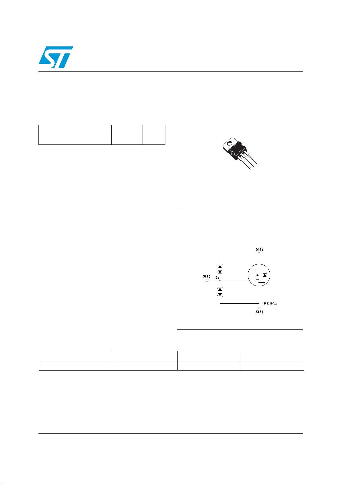
STP75NS04Z
3
2
1
TO-220
This fully clamped MOSFET is produced by using
the latest advanced Company’s Mesh Overlay
process which is based on a novel strip layout.
The inherent benefits of a new technology
coupled with the extra clamping capabilities make
this product particularly suitable for the harshest
operation conditions such as those encoured in
power tools. Any other application requiring extra
ruggedness is also recommended.
Applications
■ Switching application
■ Power tools
Order codes
Part number Marking Package Packaging
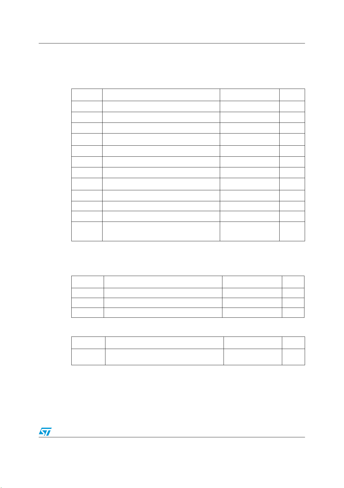
Internal schematic diagram
STP75NS04Z P75NS04Z TO-220 Tube
June 2006 Rev 1 1/12
www.st.com
12

Contents STP75NS04Z
Contents
1 Electrical ratings . . . . . . . . . . . . . . . . . . . . . . . . . . . . . . . . . . . . . . . . . . . . 3
2 Electrical characteristics . . . . . . . . . . . . . . . . . . . . . . . . . . . . . . . . . . . . . 4
2.1 Electrical characteristics (curves) . . . . . . . . . . . . . . . . . . . . . . . . . . . . . 6
3 Test circuit . . . . . . . . . . . . . . . . . . . . . . . . . . . . . . . . . . . . . . . . . . . . . . . . 8
4 Package mechanical data . . . . . . . . . . . . . . . . . . . . . . . . . . . . . . . . . . . . . 9
5 Revision history . . . . . . . . . . . . . . . . . . . . . . . . . . . . . . . . . . . . . . . . . . . 11
2/12
STP75NS04Z Electrical ratings
1 Electrical ratings
Table 1. Absolute maximum ratings
Symbol Parameter Value Unit
I
DM
P
V
V
V
I
I
I
D
I
DG
GS
TOT
DS
DG
GS
(1)
D
Drain-source voltage (VGS = 0)
Drain-gate voltage (VGS = 0)
Gate-source voltage Clamped V
Drain current (continuous) at TC = 25°C
Drain current (continuous) at TC = 100°C
Drain gate current (continuos) ±50 mA
Gate source current (continuos) ±50 mA
(2)
Drain current (pulsed) 320 A
Total dissipation at TC = 25°C
Derating factor 0.73 W/°C
V
ESD
T
T
stg
1. Current limited by wire bonding
2. Pulse with limited by safe operating area
Gate-source ESD (HBM-C=100pF, R=1.5KΩ) ±8 kV
Operating junction temperature
j
Storage temperature
Table 2. Thermal data
Clamped V
Clamped V
80 A
63 A
110 W
-55 to 175 °C
Symbol Parameter Value Unit
R
thj-case
R
thj-amb
T
Thermal resistance junction-case Max 1.36 °C/W
Thermal resistance junction-ambient Max 62.5 °C/W
Maximum lead temperature for soldering purpose 300 °C
l
Table 3. Avalanche data
Symbol Parameter Value Unit
E
AS
Single pulse avalanche energy (starting Tj=25°C,
, VDD=25V)
I
D=IAR
470 mJ
3/12
Electrical characteristics STP75NS04Z
2 Electrical characteristics
(T
=25°C unless otherwise specified)
CASE
Table 4. On/off states
Symbol Parameter Test condictions Min. Typ. Max. Unit
V
(BR)DSS
I
DSS
I
GSS
V
GSS
V
GS(th)
R
DS(on)
Drain-source breakdown
voltage
Zero gate voltage drain
current (V
GS
= 0)
Gate body leakage current
(VDS = 0)
Gate threshold breakdown
voltage
Gate threshold voltage
Static drain-source on
resistance
= 1mA, VGS= 0
I
D
= 16V
V
DS
V
= ±10V
GS
IGS= ±100µA
= VGS, ID = 250µA
V
DS
VGS= 10V, ID= 40A
33 V
1µA
2 µA
18 V
234V
711mΩ
Table 5. Dynamic
Symbol Parameter Test condictions Min. Typ. Max. Unit
(1)
g
fs
C
C
C
Q
Q
Q
1. Pulsed: pulse duration=300µs, duty cycle 1.5%
Forward transconductance
Input capacitance
iss
Output capacitance
oss
Reverse transfer
rss
capacitance
g
Total gate charge
Gate-source charge
gs
Gate-drain charge
gd
=15V, ID = 15A
V
DS
= 25V, f = 1 MHz,
V
DS
=0
V
GS
= 20V, ID= 80 A,
V
DD
= 10 V
V
GS
(see Figure 13)
50 S
1860
628
196
50
14
16
pF
pF
pF
nC
nC
nC
4/12

STP75NS04Z Electrical characteristics
Table 6. Switching on/off
Symbol Parameter Test condictions Min. Typ. Max. Unit
= 20V, ID = 40A
V
t
d(on)
t
d(off)
Turn-on delay time
t
Rise time
r
Turn-off delay time
t
Fall time
f
DD
= 4.7 Ω, VGS= 10V,
R
G
(see Figure 12)
V
= 20V, ID = 40A
DD
= 4.7 Ω, VGS= 10V,
R
G
(see Figure 12)
16
248
53
85
ns
ns
ns
ns
Table 7. Source drain diode
Symbol Parameter Test condictions Min. Typ. Max. Unit
I
SD
Source-drain current
(1)
I
SDM
V
SD
Q
I
RRM
1. Pulse width limited by safe operating area
2. Pulsed: pulse duration=300µs, duty cycle 1.5%
Source-drain current (pulsed)
(2)
Forward on Voltage
t
rr
Reverse recovery time
Reverse recovery charge
rr
Reverse recovery current
I
=80A, VGS=0
SD
=80A, di/dt = 100A/µs,
I
SD
=30V, Tj=150°C
V
DD
(see Figure 17)
53
91
3.4
80
320AA
1.5 V
ns
nC
A
5/12

Electrical characteristics STP75NS04Z
2.1 Electrical characteristics (curves)
Figure 1. Safe operating area Figure 2. Thermal impedance
Figure 3. Output characterisics Figure 4. Transfer characteristics
Figure 5. Normalized B
vs temperature Figure 6. Static drain-source on resistance
VDSS
6/12

STP75NS04Z Electrical characteristics
Figure 7. Gate charge vs gate-source voltage Figure 8. Capacitance variations
Figure 9. Normalized gate threshold voltage
vs temperature
Figure 11. Source-drain diode forward
characteristics
Figure 10. Normalized on resistance vs
temperature
7/12

Test circuit STP75NS04Z
3 Test circuit
Figure 12. Switching times test circuit for
resistive load
Figure 14. Test circuit for inductive load
switching and diode recovery times
Figure 13. Gate charge test circuit
Figure 15. Unclamped inductive load test
circuit
Figure 16. Unclamped inductive waveform Figure 17. Switching time waveform
8/12

STP75NS04Z Package mechanical data
4 Package mechanical data
In order to meet environmental requirements, ST offers these devices in ECOPACK®
packages. These packages have a Lead-free second level interconnect . The category of
second level interconnect is marked on the package and on the inner box label, in
compliance with JEDEC Standard JESD97. The maximum ratings related to soldering
conditions are also marked on the inner box label. ECOPACK is an ST trademark.
ECOPACK specifications are available at: www.st.com
9/12

Package mechanical data STP75NS04Z
TO-220 MECHANICAL DATA
DIM.
A 4.40 4.60 0.173 0.181
b 0.61 0.88 0.024 0.034
b1 1.15 1.70 0.045 0.066
c 0.49 0.70 0.019 0.027
D 15.25 15.75 0.60 0.620
E 10 10.40 0.393 0.409
e 2.40 2.70 0.094 0.106
e1 4.95 5.15 0.194 0.202
F 1.23 1.32 0.048 0.052
H1 6.20 6.60 0.244 0.256
J1 2.40 2.72 0.094 0.107
L 13 14 0.511 0.551
L1 3.50 3.93 0.137 0.154
L20 16.40 0.645
L30 28.90 1.137
øP 3.75 3.85 0.147 0.151
Q 2.65 2.95 0.104 0.116
MIN. TYP MAX. MIN. TYP. MAX.
mm. inch
10/12

STP75NS04Z Revision history
5 Revision history
Table 8. Revision history
Date Revision Changes
06-Jun-2006 1 First release
11/12

STP75NS04Z
Please Read Carefully:
Information in this document is provided solely in connection with ST products. STMicroelectronics NV and its subsidiaries (“ST”) reserve the
right to make changes, corrections, modifications or improvements, to this document, and the products and services described herein at any
time, without notice.
All ST products are sold pursuant to ST’s terms and conditions of sale.
Purchasers are solely responsible for the choice, selection and use of the ST products and services described herein, and ST assumes no
liability whatsoever relating to the choice, selection or use of the ST products and services described herein.
No license, express or implied, by estoppel or otherwise, to any intellectual property rights is granted under this document. If any part of this
document refers to any third party products or services it shall not be deemed a license grant by ST for the use of such third party products
or services, or any intellectual property contained therein or considered as a warranty covering the use in any manner whatsoever of such
third party products or services or any intellectual property contained therein.
UNLESS OTHERWISE SET FORTH IN ST’S TERMS AND CONDITIONS OF SALE ST DISCLAIMS ANY EXPRESS OR IMPLIED
WARRANTY WITH RESPECT TO THE USE AND/OR SALE OF ST PRODUCTS INCLUDING WITHOUT LIMITATION IMPLIED
WARRANTIES OF MERCHANTABILITY, FITNESS FOR A PARTICULAR PURPOSE (AND THEIR EQUIVALENTS UNDER THE LAWS
OF ANY JURISDICTION), OR INFRINGEMENT OF ANY PATENT, COPYRIGHT OR OTHER INTELLECTUAL PROPERTY RIGHT.
UNLESS EXPRESSLY APPROVED IN WRITING BY AN AUTHORIZE REPRESENTATIVE OF ST, ST PRODUCTS ARE NOT DESIGNED,
AUTHORIZED OR WARRANTED FOR USE IN MILITARY, AIR CRAFT, SPACE, LIFE SAVING, OR LIFE SUSTAINING APPLICATIONS,
NOR IN PRODUCTS OR SYSTEMS, WHERE FAILURE OR MALFUNCTION MAY RESULT IN PERSONAL INJURY, DEATH, OR
SEVERE PROPERTY OR ENVIRONMENTAL DAMAGE.
Resale of ST products with provisions different from the statements and/or technical features set forth in this document shall immediately void
any warranty granted by ST for the ST product or service described herein and shall not create or extend in any manner whatsoever, any
liability of ST.
ST and the ST logo are trademarks or registered trademarks of ST in various countries.
Information in this document supersedes and replaces all information previously supplied.
The ST logo is a registered trademark of STMicroelectronics. All other names are the property of their respective owners.
© 2006 STMicroelectronics - All rights reserved
STMicroelectronics group of companies
Australia - Belgium - Brazil - Canada - China - Czech Republic - Finland - France - Germany - Hong Kong - India - Israel - Italy - Japan -
Malaysia - Malta - Morocco - Singapore - Spain - Sweden - Switzerland - United Kingdom - United States of America
www.st.com
12/12
 Loading...