

查询STP16NB25供应商
STP16NB25
STP16NB25FP
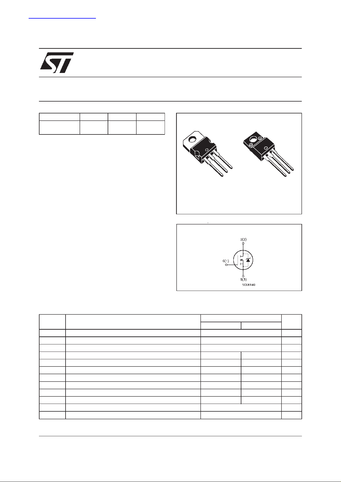
N - CHANNEL 250V- 0.220Ω - 16A - TO-220/TO-220FP
PowerMESH MOSFET
TYPE V
STP16NB25
ST P16NB25FP
■ TYPICALR
■ EXTREMELYHIGH dv/dt CAPABILITY
■ 100%AVALANCHETESTED
■ VERYLOW INTRINSIC CAPACITANCES
■ GATECHARGE MINIMIZED
DS(on)
DSS
250 V
250 V
= 0.220 Ω
DESCRIPTION
Using the latest high voltage MESH OVERLAY
process, STMicroelectronics has designed an
advanced family of power MOSFETs with
outstanding performances. The new patent
pending strip layout coupled with the Company’s
proprietary edge termination structure, gives the
lowest RDS(on) per area, exceptional avalanche
and dv/dt capabilities and unrivalled gate charge
and switching characteristics.
R
DS(on)
<0.28Ω
<0.28Ω
I
D
16 A
8A
3
2
1
TO-220 TO-220FP
INTERNAL SCHEMATIC DIAGRAM
3
2
1
APPLICATIONS
■ HIGHCURRENT, HIGH SPEED SWITCHING
■ UNINTERRUPTIBLEPOWERSUPPLY(UPS)
■ DC-DC& DC-ACCONVERTERSFOR
TELECOM,INDUSTRIAL ANDCONSUMER
ENVIRONMENT
ABSOLUTE MAXIMUM RATINGS
Symbol Parameter Value Unit
STP 16NB25 ST P16NB25F P
V
V
V
I
DM
P
dv/dt(
V
T
(•) Pulse width limited by safe operating area (1)ISD≤ 16A, di/dt ≤ 200A/µs, VDD≤ V
Dra in- sour c e Volt age (VGS= 0) 250 V
DS
Dra in- gat e Volt age (RGS=20kΩ) 250 V
DGR
Gat e-source Voltage ± 30 V
GS
Dra in Cu rr ent (cont inuous) at Tc=25oC168A
I
D
Dra in Cu rr ent (cont inuous) at Tc=100oC105A
I
D
(•) Drain Cu rr ent ( p uls ed ) 64 32 A
Tot al Dis sipation at Tc=25oC 140 45 W
tot
Der ati ng Fact or 1.12 0.36 W/
) P eak Diode Re c overy voltage sl ope 5.5 5.5 V/ns
1
Insulation W ithsta nd Voltage (DC) ----- 2000 V
ISO
St orage T em pe r at ure -65 to 150
stg
Max. Operating Junction Temperat ur e 150
T
j
(BR)DSS
,Tj≤T
JMAX
o
C
o
C
o
C
March 1999
1/9
STP16NB25/FP
THERMAL DATA
TO-220 TO 220FP
R
thj-case
R
thj-amb
R
thc-sink
T
AVALANCHE CHARACTERISTICS
Symbol Parameter Max V alue Unit
I
AR
E
Ther mal Res istance Junct ion-case Ma x 0.9 2.77
Ther mal Res istance Junct ion-ambient Max
Ther mal Res istance C as e -s ink Ty p
Maximum Lead Tempera tur e For Soldering Purpose
l
Avalanche Current, Repetitive or Not-Repetitive
(pulse width limited by T
Single Pul s e A v alan che Energy
AS
(starting T
=25oC, ID=IAR,VDD=50V)
j
max)
j
62.5
0.5
300
16 A
250 mJ
o
C/W
o
C/W
o
C/W
o
C
ELECTRICAL CHARACTERISTICS
=25oC unless otherwisespecified)
(T
case
OFF
Symbol Parameter Test Conditions Min. Typ. Max. Unit
V
(BR)DSS
Drain-source
ID=250µAVGS= 0 250 V
Break dow n Voltage
I
DSS
I
GSS
Zero Gate Voltage
Drain Current ( V
GS
Gat e- bod y Leak ag e
Current (V
DS
=0)
=0)
V
=MaxRating
DS
=MaxRating Tc=125oC
V
DS
V
=± 30 V
GS
1
10
100 nA
±
ON(∗)
Symbol Parameter Test Conditions Min. Typ. Max. Unit
V
GS(th)
R
DS(on)
Gate Threshold Voltage VDS=VGSID= 250µA 345V
Sta t ic Drain-s ource On
VGS=10V ID= 8 A 0.22 0.28
Resistance
I
D(on)
On StateDrain Current VDS>I
D(on)xRDS(on)max
16 A
VGS=10V
DYNAMIC
Symbol Parameter Test Conditions Min. Typ. Max. Unit
g
(∗)Forward
fs
Tr ansc on duc tance
C
C
C
Input Capaci t anc e
iss
Out put Capac it ance
oss
Reverse Transfer
rss
Capacit a nc e
VDS>I
D(on)xRDS(on)maxID
=8 A 4 S
VDS=25V f=1MHz VGS= 0 1000
250
40
µA
µA
Ω
pF
pF
pF
2/9
STP16NB25/FP
ELECTRICAL CHARACTERISTICS
(continued)
SWITCHINGON
Symbol Parameter Test Conditions Min. Typ. Max. Unit
t
d(on)
t
Tur n-on Delay Time
Rise Tim e
r
VDD=125V ID=8A
R
=4.7
G
Ω
VGS=10V
12
12
(Resis t iv e Load, s ee fig. 3)
Q
Q
Q
Tot al Gate C harge
g
Gat e- Source Charg e
gs
Gate-Drain Charge
gd
VDD= 200 V ID=16A VGS=10V 29
9
11
38 nC
SWITCHINGOFF
Symbol Parameter Test Conditions Min. Typ. Max. Unit
t
d(off)
Tur n-of f Dela y T im e
t
Fall T ime
f
VDD=125V ID=8A
=4.7 Ω VGS=10V
R
G
35
8
(Resis t iv e Load, s ee fig. 3)
t
r(Voff)
t
t
Off-voltage Rise T im e
Fall T ime
f
Cross-over Time
c
V
R
=200V ID=16A
CLAM P
=4.7 Ω VGS=10V
G
(Indu ct iv e Load, se e fig. 5)
10
9
20
SOURCEDRAINDIODE
Symbol Parameter Test Conditions Min. Typ. Max. Unit
I
V
I
SDM
SD
Q
I
RRM
SD
t
Source-drain Current
(•)
Source-drain Current
16
64
(pulsed)
(∗)ForwardOnVoltage ISD=16A VGS=0 1.5 V
Reverse Recovery
rr
Time
Reverse Recovery
rr
ISD= 16 A di/dt = 100 A /µs
=50V Tj=150oC
V
DD
(see test circuit, fig. 5)
210
1.5
Charge
Reverse Recovery
14
Current
ns
ns
nC
nC
ns
ns
ns
ns
ns
A
A
ns
µC
A
(∗) Pulsed:Pulse duration = 300 µs, duty cycle 1.5 %
(•) Pulse width limited by safeoperating area
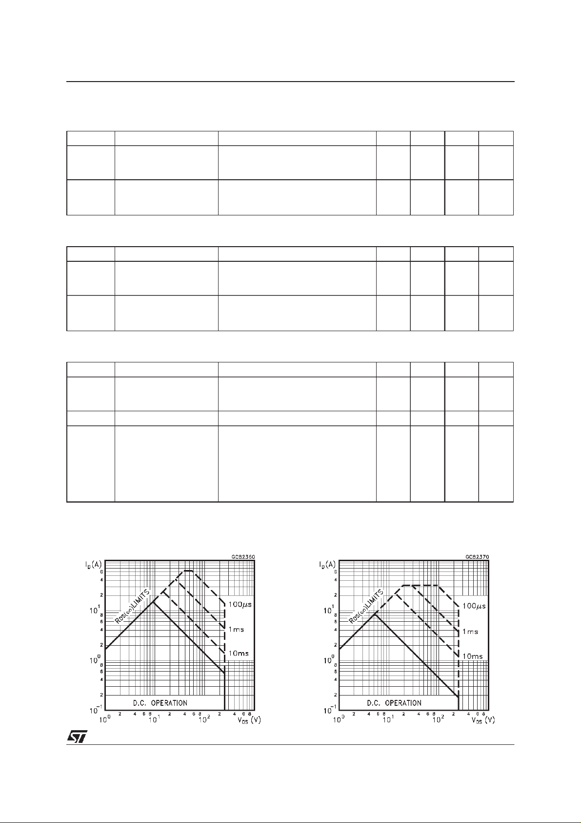
SafeOperating Area for TO-220 SafeOperating Area for TO-220FP
3/9
 Loading...