

Low voltage 16-bit constant current LED sink driver
Features
■ 16 constant current output channels
■ Adjustable output current through external
resistor
■ Output current: 3-40 mA
■ Serial data in/parallel data ouT
■ 3.3 V or 5 V supply voltage
■ Max clock frequency 30 MHz
■ Schmitt-trigger input
■ ESD protection 2 kV HBM
■ Thermal shutdown
Description
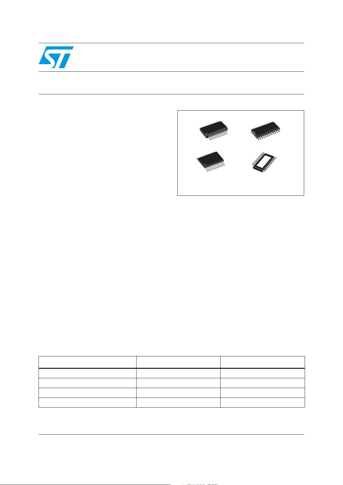
QSOP-24
TSSOP24
STP16CPP05
SO-24
TSSOP24
(exposed pad)
The STP16CPP05 is a monolithic, low voltage,
low current power 16-bit shift register designed for
LED panel displays. The STP16CPP05 contains a
16-bit serial-in, parallel-out shift register that
feeds a 16-bit, D-type storage register. In the
output stage, sixteen regulated current sources
provide from 3 mA to 40 mA constant current to
drive the LEDs.
The output current setup time is 40 ns (typ), thus
improving the system performance.
The LEDs' brightness can be controlled by using
an external resistor to adjust the STP16CPP05
output current.
Table 1. Device summary
Order codes Package Packaging
STP16CPP05MTR SO-24 1000 parts per reel
STP16CPP05TTR TSSOP24 2500 parts per reel
STP16CPP05XTTR TSSOP24 exposed pad 2500 parts per reel
The STP16CPP05 guarantees a 20 V output
driving capability, allowing users to connect more
LEDs in series.The high clock frequency, 30 MHz,
makes the device suitable for high data rate
transmission. The 3.3 V voltage supply is useful in
applications that interface with a 3.3 V micro
controller.
STP16CPP05PTR QSOP-24 2500 parts per reel
October 2009 Doc ID 15379 Rev 2 1/28
www.st.com
28

Contents STP16CPP05
Contents
1 Summary description . . . . . . . . . . . . . . . . . . . . . . . . . . . . . . . . . . . . . . . . 3
1.1 Pin connection and description . . . . . . . . . . . . . . . . . . . . . . . . . . . . . . . . . 3
2 Electrical ratings . . . . . . . . . . . . . . . . . . . . . . . . . . . . . . . . . . . . . . . . . . . . 5
2.1 Absolute maximum ratings . . . . . . . . . . . . . . . . . . . . . . . . . . . . . . . . . . . . . 5
2.2 Thermal data . . . . . . . . . . . . . . . . . . . . . . . . . . . . . . . . . . . . . . . . . . . . . . . 5
2.3 Recommended operating conditions . . . . . . . . . . . . . . . . . . . . . . . . . . . . . 6
3 Electrical characteristics . . . . . . . . . . . . . . . . . . . . . . . . . . . . . . . . . . . . . 7
4 Equivalent circuit and outputs . . . . . . . . . . . . . . . . . . . . . . . . . . . . . . . . . 9
5 Timing diagrams . . . . . . . . . . . . . . . . . . . . . . . . . . . . . . . . . . . . . . . . . . . 11
6 Typical characteristics . . . . . . . . . . . . . . . . . . . . . . . . . . . . . . . . . . . . . . 14
7 Test circuit . . . . . . . . . . . . . . . . . . . . . . . . . . . . . . . . . . . . . . . . . . . . . . . . 17
8 Package mechanical data . . . . . . . . . . . . . . . . . . . . . . . . . . . . . . . . . . . . 20
9 Revision history . . . . . . . . . . . . . . . . . . . . . . . . . . . . . . . . . . . . . . . . . . . 28
2/28 Doc ID 15379 Rev 2
STP16CPP05 Summary description
1 Summary description
Table 2. Typical current accuracy
Output voltage
Current accuracy
Between bits Between ICs
≥ 1.3 V ± 1.2% ±5% ≥ 5 to 40 mA 3.3 V to 5 V 25 °C
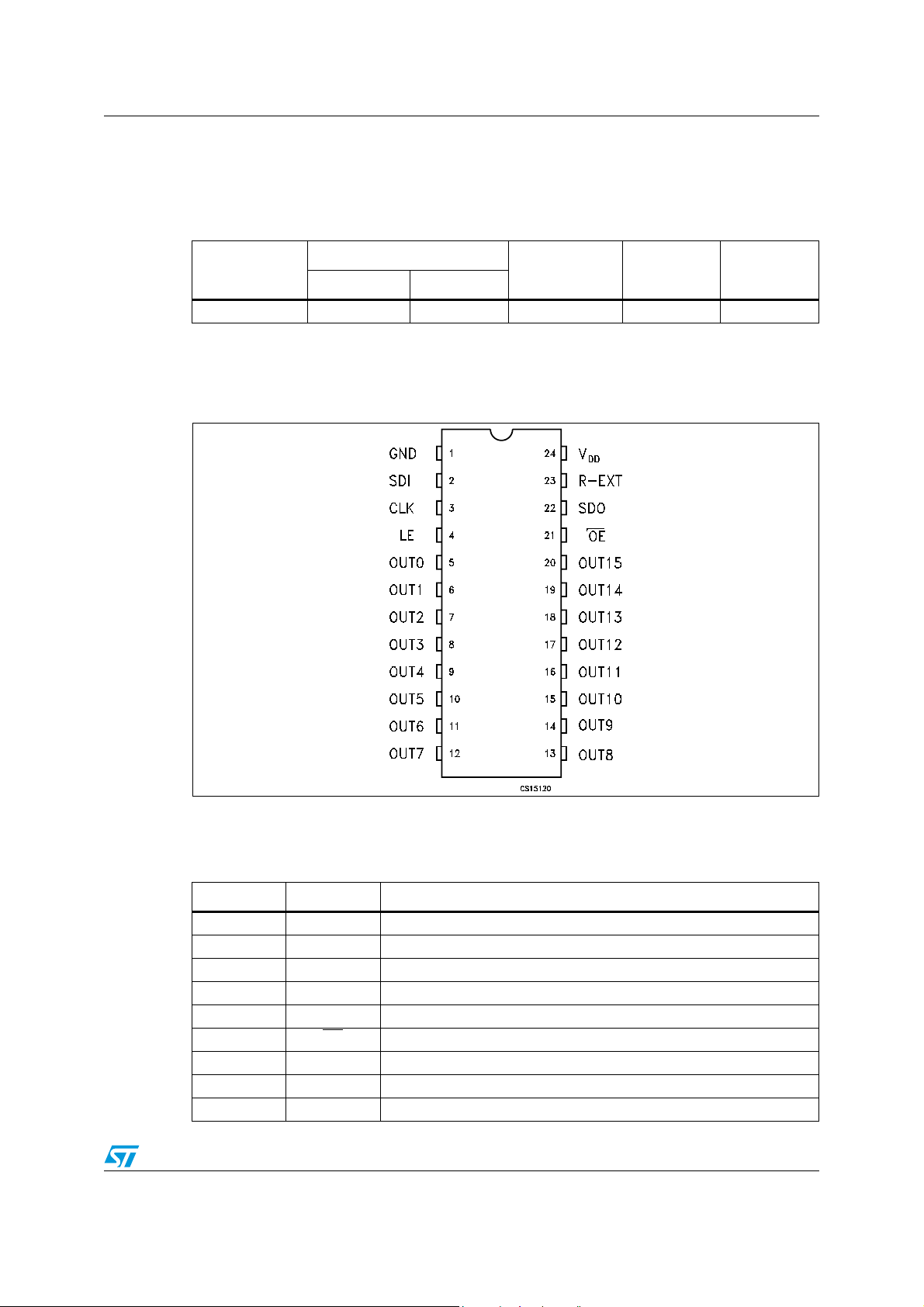
1.1 Pin connection and description
Figure 1. Pin connection
Output current
V
DD
Temperature
Note: The exposed pad should be electrically connected to a metal land electrically isolated or
connected to ground.
Table 3. Pin description
Pin N° Symbol Name and function
1 GND Ground terminal
2 SDI Serial data input terminal
3 CLK Clock input terminal
4 LE Latch input terminal
5-20 OUT 0-15 Output terminal
21 OE
22 SDO Serial data out terminal
23 R-EXT Input terminal of an external resistor for constant current programing
24 V
DD
Input terminal of output enable (active low)
Supply voltage terminal
Doc ID 15379 Rev 2 3/28
Electrical ratings STP16CPP05
2 Electrical ratings
2.1 Absolute maximum ratings
Stressing the device above the rating listed in the “absolute maximum ratings” table may
cause permanent damage to the device. These are stress ratings only and operation of the
device at these or any other conditions above those indicated in the operating sections of
this specification is not implied. Exposure to absolute maximum rating conditions for
extended periods may affect device reliability.
Table 4. Absolute maximum ratings
Symbol Parameter Value Unit
V
V
I
V
I
GND
f
CLK
DD
O
Supply voltage 0 to 7 V
Output voltage -0.5 to 20 V
O
Output current 50 mA
Input voltage -0.4 to VDD+0.4 V
I
GND terminal current 800 mA
Clock frequency 50 MHz
2.2 Thermal data
Table 5. Thermal data
Symbol Parameter Value Unit
T
OPR
T
STG
R
thJC
1. The exposed pad should be soldered directly to the PCB to realize the thermal benefits.
Operating temperature range -40 to +125 °C
Storage temperature range -55 to +150 °C
Thermal resistance junction-case
SO-24 60 °C/W
TSSOP24 85 °C/W
(1)
TSSOP24
Exposed Pad
QSOP-24 72 °C/W
37.5 °C/W
4/28 Doc ID 15379 Rev 2

STP16CPP05 Electrical ratings
2.3 Recommended operating conditions
Table 6. Recommended operating conditions at 25 °C
Symbol Parameter Test conditions Min Typ Max Unit
V
V
I
I
V
V
t
wLAT
t
wCLK
t
wEN
t
SETUP(D)
t
HOLD(D)
t
SETUP(L)
f
CLK
1. If the device is connected in cascade, it may not be possible achieve the maximum data transfer. Please
considered the timings carefully.
Supply voltage 3.0 5.5 V
DD
Output voltage 20 V
O
Output current OUTn 3 40 mA
I
O
Output current SERIAL-OUT +1 mA
OH
Output current SERIAL-OUT -1 mA
OL
Input voltage 0.7 V
IH
Input voltage -0.3 0.3 V
IL
LE pulse width
DD
20 ns
CLK pulse width 16 ns
OE pulse width 70 ns
VDD = 3.3 V to 5.0 V
Setup time for DATA 5 ns
Hold time for DATA 5 ns
Setup time for LATCH 15 ns
Clock frequency Cascade operation
(1)
VDD+0.3 V
DD
30 MHz
V
Doc ID 15379 Rev 2 5/28
Electrical characteristics STP16CPP05
3 Electrical characteristics
VDD = 3.3 V to 5 V, T = 25 °C, unless otherwise specified.
Table 7. Electrical characteristics
Symbol Parameter Test conditions Min Typ Max Unit
V
IH
V
IL
I
OH
V
OL
V
OH
I
OL1
OL2
I
OL3
ΔI
OL1
OL2
ΔI
OL3
R
SIN(up)
R
SIN(down)
I
DD(OFF1)
I
DD(OFF2)
I
DD(ON1)
I
DD(ON2)
Input voltage high level 0.7V
DD
Input voltage low level GND 0.3V
V
DD
DD
V
V
Output leakage current VOH = 20 V 0.15 1 μA
Output voltage
(Serial-OUT)
Output voltage
(Serial-OUT)
Output current
Output current error
between bit
(All Output ON)
= 1 mA 0.4 V
I
OL
= -1 mA VDD-0.4V V
I
OH
= 0.3 V, R
V
O
VO = 0.3 V, R
VO = 1.3 V, R
VO = 0.3 V, IO = 5 mA
= 4 kΩ
R
EXT
VO = 0.3 V, IO = 20 mA
R
= 980 Ω
EXT
VO = 1.3 V, IO = 40 mA
R
= 490 Ω
EXT
= 4 kΩ 4.75 5 5.25
ext
= 980 Ω 19 20 21
ext
= 490 Ω 38 40 42
ext
± 1.2 ± 5
± 0.5 ± 3
± 1.0 ± 3
mAI
%ΔI
Pull-up resistor 150 300 600 kΩ
Pull-down resistor 100 200 400 kΩ
R
= 980
EXT
OUT 0 to 15 = OFF
5.4 7.5
Supply current (OFF)
R
= 490
EXT
OUT 0 to 15 = OFF
8.0 9.5
mA
R
= 980
EXT
OUT 0 to 15 = ON
5.5 7.5
Supply current (ON)
R
= 490
EXT
OUT 0 to 15 = ON
8.1 9.5
Thermal Thermal protection 170 °C
6/28 Doc ID 15379 Rev 2
STP16CPP05 Electrical characteristics
V
= 5 V, T = 25 °C, unless otherwise specified.
DD
Table 8. Switching characteristics
Symbol Parameter Test conditions Min Typ Max Unit
V
= 3.3 V - 44 58
t
PLH1
t
PLH2
t
PLH3
t
Propagation delay time,
CLK-OUTn
Propagation delay time,
LE-OUTn, OE = L
Propagation delay time,
OE-OUTn, LE = H
Propagation delay time,
PLH
CLK-SDO
, LE = H, OE = L
Propagation delay time,
t
PHL1
t
PHL2
t
PHL3
t
PHL
CLK-OUTn
OE = L
Propagation delay time,
LE-OUTn
Propagation delay time,
OE-OUTn, LE = H
Propagation delay time,
CLK-SDO
, LE = H,
, OE = L
V
= V
IH
DD
VIL = GND CL = 10 pF
= 20 mA VL = 3.0 V
I
O
R
= 1 KΩ RL = 60 Ω
EXT
Output rise time
t
10~90% of current
ON
waveform
Output fall time
t
90~10% of current
OFF
waveform
CLK rise time
t
r
t
CLK fall time
f
1. In order to achieve high cascade data transfer, please consider tr/tf timings carefully.
(1)
(1)
DD
= 5 V - 24 32
V
DD
= 3.3 V - 43 56
V
DD
= 5 V - 24 32
V
DD
= 3.3 V - 63 82
V
DD
= 5 V - 37 48
V
DD
= 3.3 V - 17 22
V
DD
= 5 V - 11 14
V
DD
V
= 3.3 V - 22 28
DD
= 5 V - 16 21
V
DD
VDD = 3.3 V - 19 25
= 5 V - 15 20
V
DD
= 3.3 V - 16 21
V
DD
= 5 V - 13 17
V
DD
= 3.3 V - 21 27
V
DD
= 5 V - 13 17
V
DD
VDD = 3.3 V - 26 35
= 5 V - 12 16
V
DD
VDD = 3.3 V - 4 6
= 5 V - 3 5
V
DD
-5000ns
-5000ns
ns
ns
ns
ns
ns
ns
ns
ns
ns
ns
Doc ID 15379 Rev 2 7/28
Equivalent circuit and outputs STP16CPP05
4 Equivalent circuit and outputs
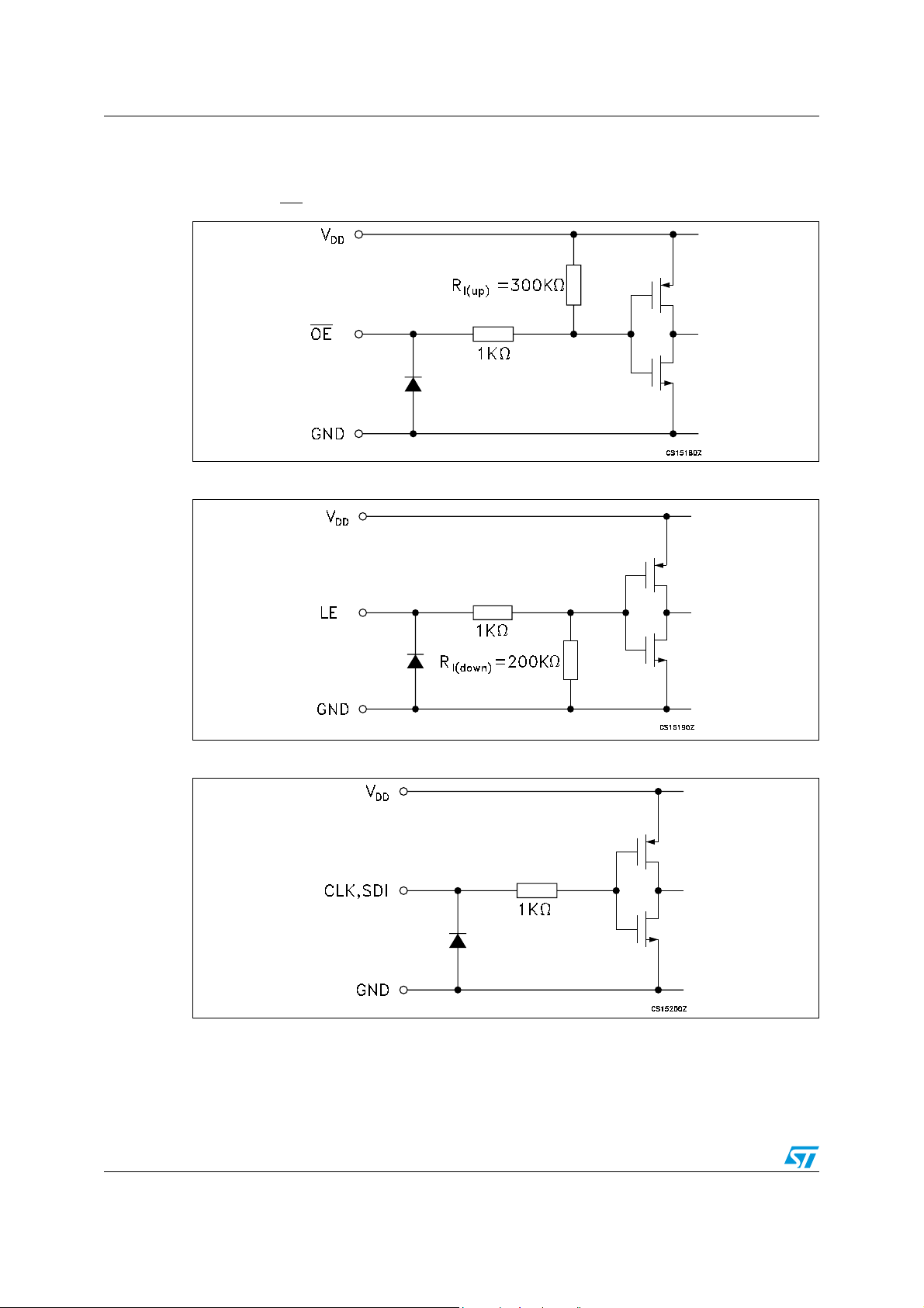
Figure 2. OE terminal
Figure 3. LE terminal
Figure 4. CLK, SDI terminal
8/28 Doc ID 15379 Rev 2
STP16CPP05 Equivalent circuit and outputs
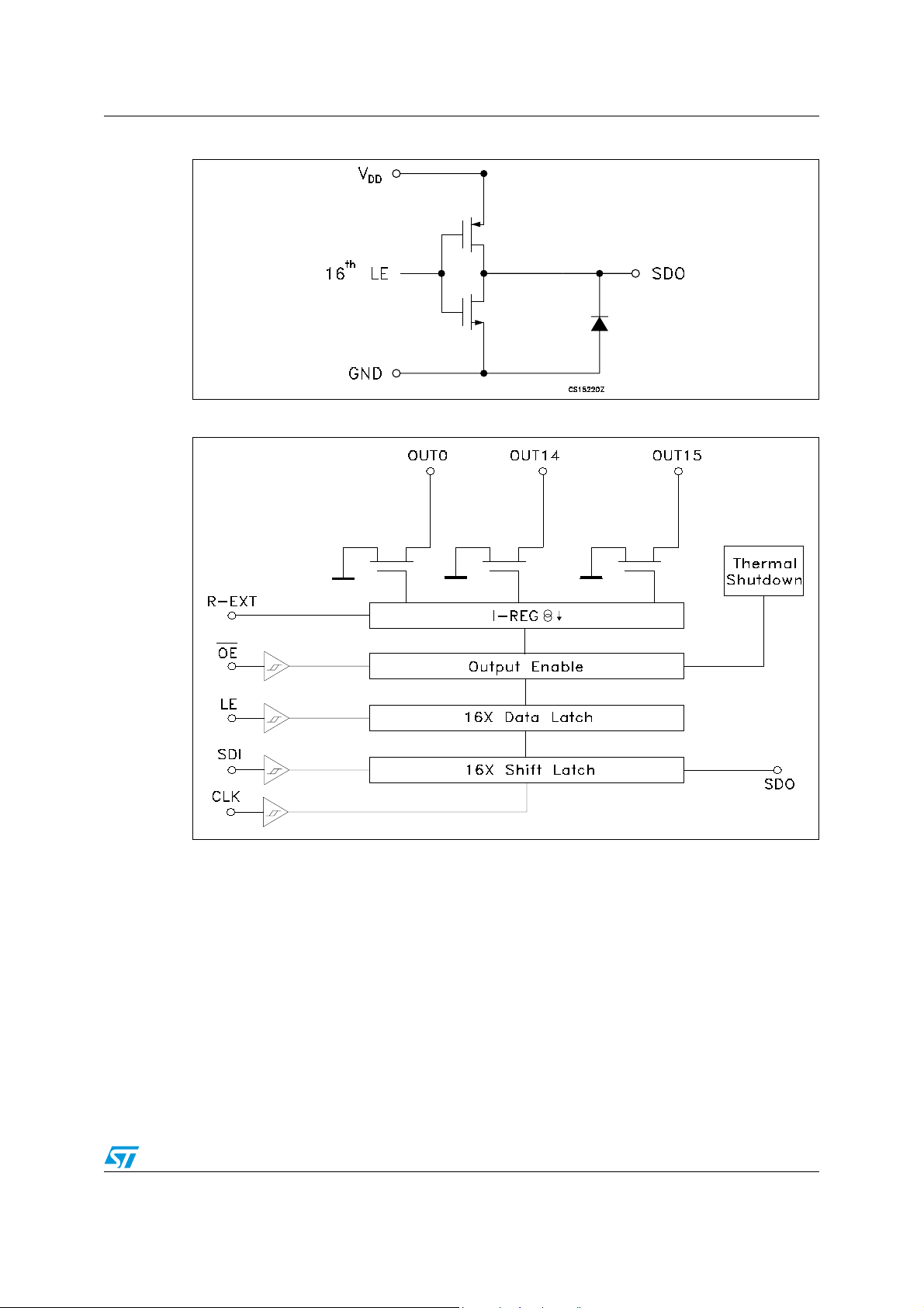
Figure 5. SDO terminal
Figure 6. Block diagram
Doc ID 15379 Rev 2 9/28
 Loading...