

查询STP16C596B1R供应商
16-BIT CONSTANT CURRENT LED SINK DRIVER
STP16C596
■ 16 CONSTANT CURRENT OUTPUT
CHANNELS
■ ADJUST ABLE OUTPUT CURRENT
THROUGH EXTERNAL RESISTOR
■ SERIAL DATA IN/PARALLEL DATA OUT
■ SERIAL OUT CHANGE STATE ON THE
FAILING EDGES OF CLOCK
■ OUTPUT CURRENT: 15-120 mA
■ 25 MHz CLOCK FREQ.
■ A VAILABLE IN HIGH THERM AL TSSOP
EXPOSED PAD
■ EFFICIENCY PACKAGE
DESCRIPTION
The STP16C596 is a monolithic, medium-voltage,
low current power 16-bit shift register designed for
LED panel d isplays. The STP16C596 contains a
16-bit serial-in, parallel-out shift register that feeds
a 16-bitD-type storage register. In the output
stage, sixteen regulated current sources are
designed to provide 15-120mA constant current to
drive the LEDs.
The serial output change state on the failing edges
of clock, this special feature will provide an
improved performance of the application when the
clock signal is skewed because the daisy chain is
too long.
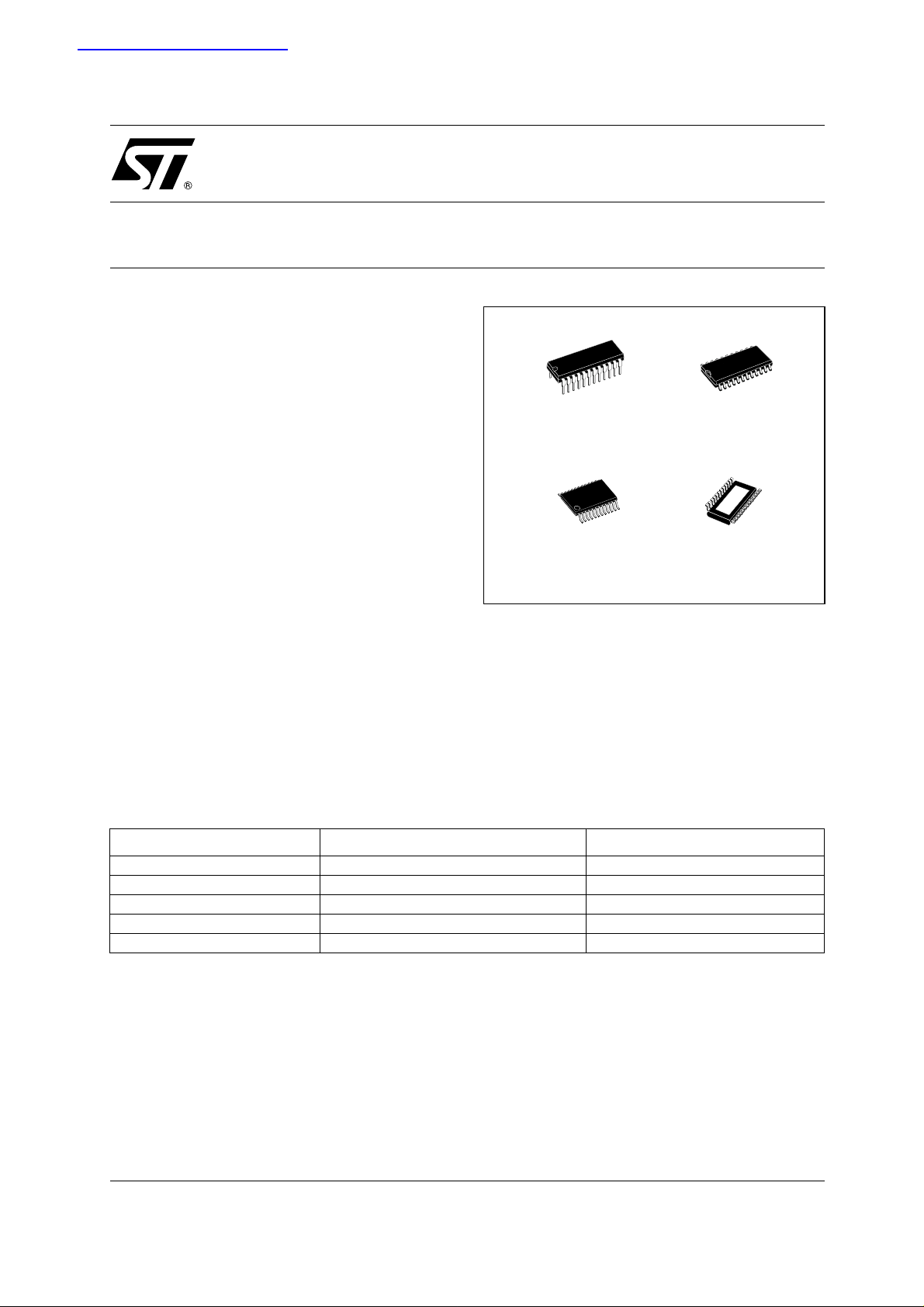
DIP-24
TSSOP24
SO-24
TSSOP24
(exposed pad)
Through an external resistor, users may adjust the
STP16C596 output current, controlling in this way
the light intensity of LEDs.
The STP16C596 guarantees a 16V output drivi ng
capability, allowing users to connect more LEDs in
series. The high clock frequency, 25 MHz, also
satisfies the system demand for high volume data
transmission. Compared wi th a standard TSSOP
package, the TSSOP exposed pad increases heat
dissipation capability by a 2.5 factor.
Table 1: Order Codes
Part Number Package Comments
STP16C596B1R DIP-24 15 parts per tube
STP16C596M SO-24 (Tube) 40 parts per tube
STP16C596MTR SO-24 (Tape & Reel) 1000 parts per reel
STP16C596TTR TSSOP24 (Tape & Reel) 2500 parts per reel
STP16C596XTTR TSSOP24 Exposed-Pad (Tape & Reel) 2500 parts per reel
Rev. 5
1/18August 2004
STP16C596
Table 2: Current Accuracy
Output Voltage
≥ 0.7V TYP. ± 3% ± 10% 15 to 120 mA
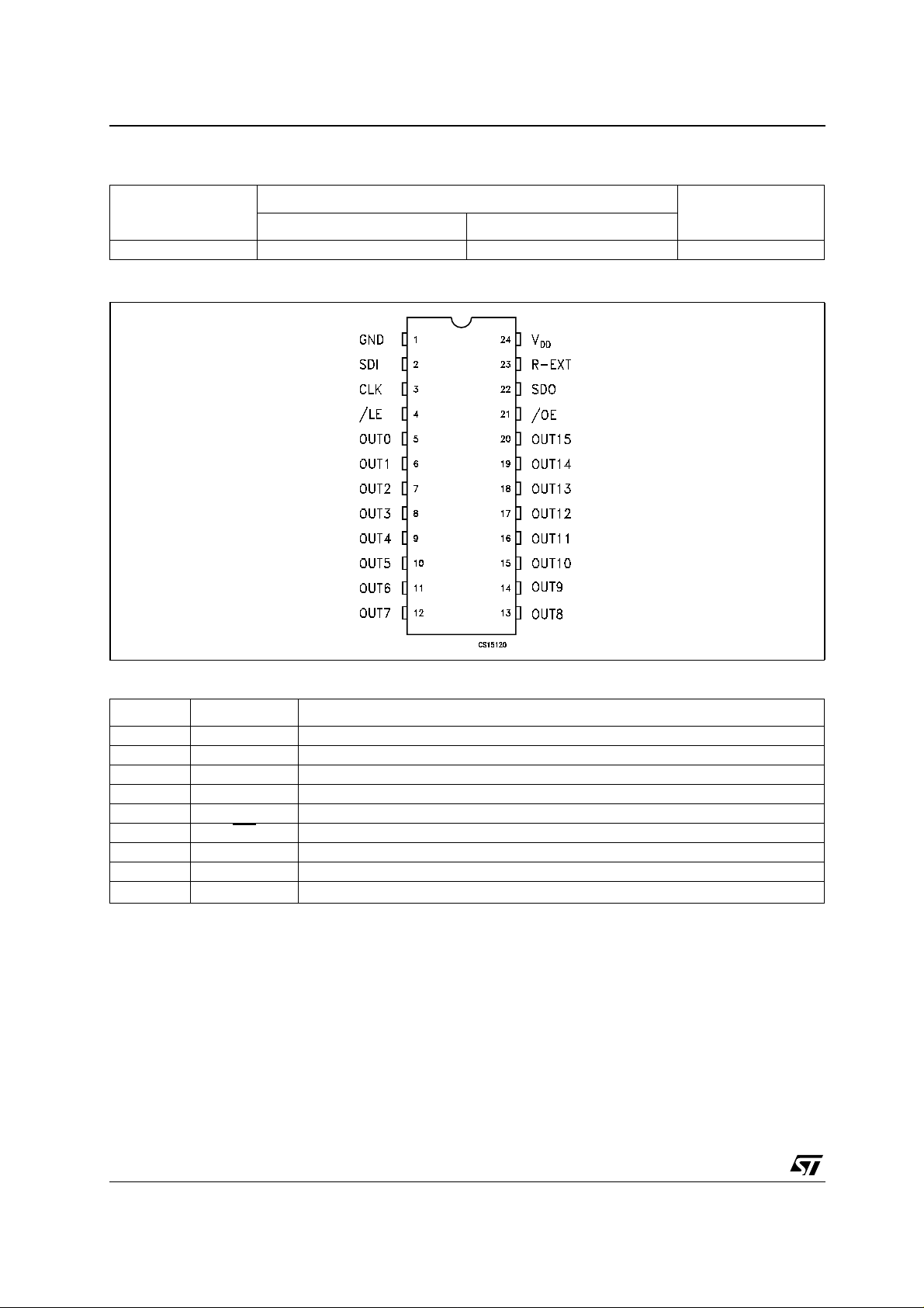
Figure 1: Pi n C onnect ion
Current accuracy
Output Current
Between bits Between ICs
Table 3: Pin Description
PIN N° Symbol Name and Function
1 GND Ground Terminal
2 SDI Serial data input terminal
3 CLK Clock input terminal
4 /LE Latch input terminal
5-20 OUT 0-15 Output terminal
21 /OE
22 SDO Serial data out terminal
23 R-EXT Input terminal of an external resistor for constant current programing
24 V
DD
Input terminal of output enable (active low)
Supply voltage terminal
2/18
STP16C596
Table 4: Absolute Maximum Ratings
Symbol Parameter Value Unit
V
V
I
V
I
GND
f
CLK
T
OPR
T
STG
Absolute Maximum Ratings are t hos e values beyond which dam age to the de vice may occu r. Under these conditions, functional opera tion
is not implied.
Table 5: Thermal Data
Supply Voltage
DD
Output Voltage
O
Output Current
O
Input Voltage -0.4 to VDD+0.4
I
GND Termin al Current
Clock Frequency
Operating Temperature Range
Storage Temperature Range
0 to 7 V
-0.5 to 16 V
120 mA
V
1920 mA
25 MHz
-40 to +125 °C
-65 to +150 °C
Symbol Parameter DIP-24 SO-24 TSSOP24
R
thj-amb
Thermal Resistance Junction-ambient
60 75 85 37.5 °C/W
TSSOP24
(exposed pad)
Table 6: Recommended Operating Conditions
Symbol Parameter Test Conditions Min. Typ. Max. Unit
V
V
I
I
V
V
t
wLAT
t
wCLK
t
wEN
t
SETUP(D)
t
HOLD(D)
t
SETUP(L)
f
CLK
Supply Voltage 4.5 5.0 5.5 V
DD
Output Voltage 16.0 V
O
Output Current OUTn 5 120 mA
I
O
Output Current SERIAL-OUT +1 mA
OH
Output Current SERIAL-OUT -1 mA
OL
Input Voltage 0.7V
IH
Input Voltage -0.3 0.3V
IL
DD
/LE Pulse Width VDD = 4.5 to 5.5V 20 ns
CLK Pulse Width 20 ns
/OE Pulse Width 400 ns
Setup Time for DATA 20 ns
Hold Time for DATA 15 ns
Setup Time for LATCH 15 ns
Clock Frequency Cascade Operation 25 MHz
VDD+0.3 V
DD
Unit
V
3/18
STP16C596
Table 7: Electrical Characteristics (VDD=5V, T = 25°C, unless otherwise specified.)
Symbol Parameter Test Conditions Min. Typ. Max. Unit
V
V
I
V
V
I
OL1
I
OL2
∆I
∆I
R
SIN(up)
R
SIN(down)
I
DD(OFF1)
I
DD(OFF2)
I
DD(OFF3)
I
DD(ON1)
I
DD(ON2)
Input Voltage High Level 0.7V
IH
Input Voltage Low Level GND 0.3V
IL
Output Leakage Current VOH = 16 V 10 µA
OH
Output Voltage (Serial-OUT) IOL = 1mA 0.4 V
OL
Output Voltage (Serial-OUT) IOH = -1mA VDD-0.4V V
OH
Output Current VO = 0.7V R
Output Current Error
OL1
between bit (All Output ON)
OL2
VO = 0.7V R
VO = 0.7V R
VO = 0.7V R
= 910 Ω 18.6 20.4 22.4 mA
EXT
= 360 Ω 45.7 50.2 55.2 mA
EXT
= 910 Ω ± 3 ± 4 %
EXT
= 360 Ω ± 3 ± 4 %
EXT
DD
Pull-up Resistor 150 300 600 KΩ
Pull-down Resistor 100 200 400 KΩ
Supply Current (OFF) R
Supply Current (ON) R
= OPEN OUT 0 to 15 = OFF 0.3 0.6 mA
EXT
R
= 470 Ω OUT 0 to 15 = OFF 5.5 7.7
EXT
R
= 250 Ω OUT 0 to 15 = OFF 10.1 14.1
EXT
= 470 Ω OUT 0 to 15 = ON 5.5 7.7
EXT
R
= 250 Ω OUT 0 to 15 = ON 10.1 14.1
EXT
V
DD
DD
V
V
Table 8: Switching Characteristics (V
=5V, T = 25°C, unless otherwise specified.)
DD
Symbol Parameter Test Conditions Min. Typ. Max. Unit
t
PLH1
t
PLH2
t
PLH3
t
PLH
t
PHL1
t
PHL2
t
PHL3
t
PHL
Propagation Delay Time,
CLK-OUTn
, /LE = H, /OE = L
Propagation Delay Time,
-OUTn, /OE = L
/LE
Propagation Delay Time,
-OUTn, /LE = H
/OE
Propagation Delay Time,
CLK-SDO
Propagation Delay Time,
CLK-OUTn
, /LE = H, /OE = L
Propagation Delay Time,
-OUTn, /OE = L
/LE
Propagation Delay Time,
-OUTn, /LE = H
/OE
Propagation Delay Time,
CLK-SDO
t
Output Rise Time 160 200 ns
r
t
Output Fall Time 15 25 ns
f
V
= 5 V VIH = V
DD
DD
VIL = GND CL = 13pF
I
= 40mA VL = 3 V
O
R
= 470 Ω RL = 65 Ω
EXT
200 280 ns
160 250 ns
145 200 ns
15 30 ns
15 30 ns
15 30 ns
45 60 ns
15 300 ns
4/18
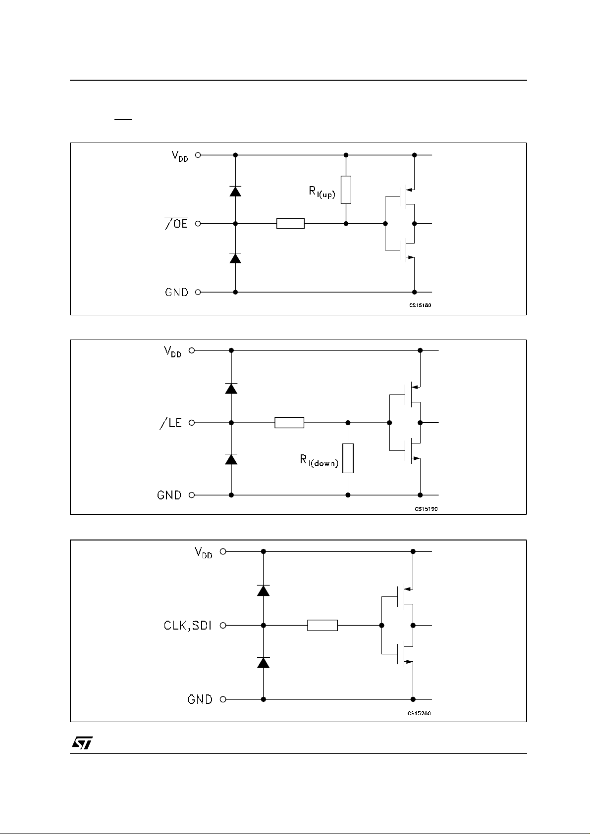
EQUIVALENT CIRCUIT OF INPUTS AND OUTPUTS
STP16C596
Figure 2: / OE
Figure 3: /LE Termin al
Terminal
Figure 4: CLK, SDI Terminal
5/18
STP16C596
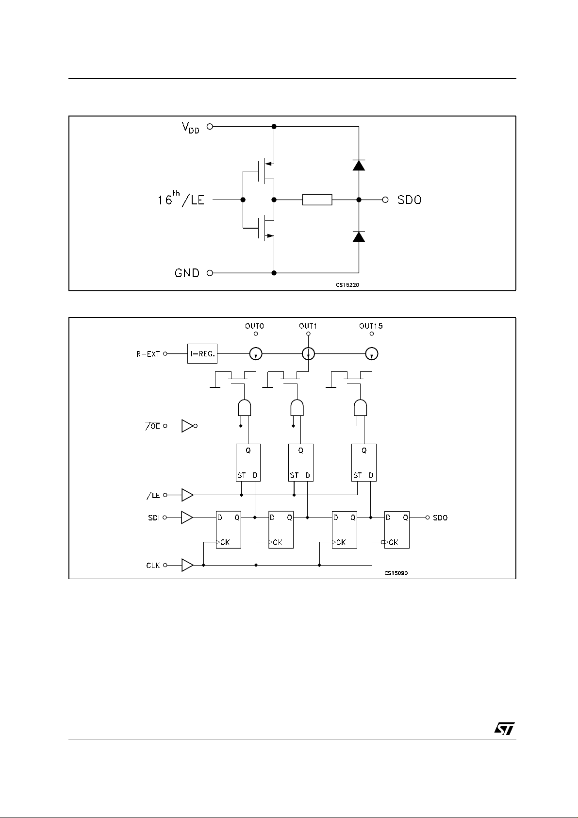
Figure 5: SDO Terminal
Figure 6: Block Diagram
6/18

STP16C596
Table 9: Truth Ta ble
CLOCK /LE /OE SERIAL-IN OUT0 .................. OUT7 .................. OUT15 SDO
H L Dn Dn ..... Dn - 7 ..... Dn -15 Dn - 15
L L Dn + 1 No Change Dn - 14
H L Dn + 2 Dn - 2 ..... Dn - 5 ..... Dn -13 Dn - 13
X L Dn + 3 Dn - 2 ..... Dn - 5 ..... Dn -13 Dn - 13
XLDn + 3 OFF Dn - 13
Note 1: OUT0 to OUT15 = ON when Dn = H; OUT0 to OUT15 = OFF when Dn = L.
Figure 7: Tim ing Diagram
Note: The latches ci rc uit holds da ta when the LE termi n a l is Low.
When LE terminal is at Hi gh l evel, latch ci rcuit doesn ’ t hold the data it passes from the input to the output.
When OE terminal is at Low level, output terminals OUT0 to OUT15 respond to the data, either ON or OFF.
When OE terminal is at High level, it switches off all the data on the output terminal.
7/18

STP16C596
Figure 8: Clock, Serial-in, Serial-out
Figure 9: Clock, Serial-in, Latch, Enable, Outputs
8/18

Figure 10: O ut puts
TEST CIRCUIT
Figure 11: DC Characteristic
STP16C596
Figure 12: AC Characteristic
9/18
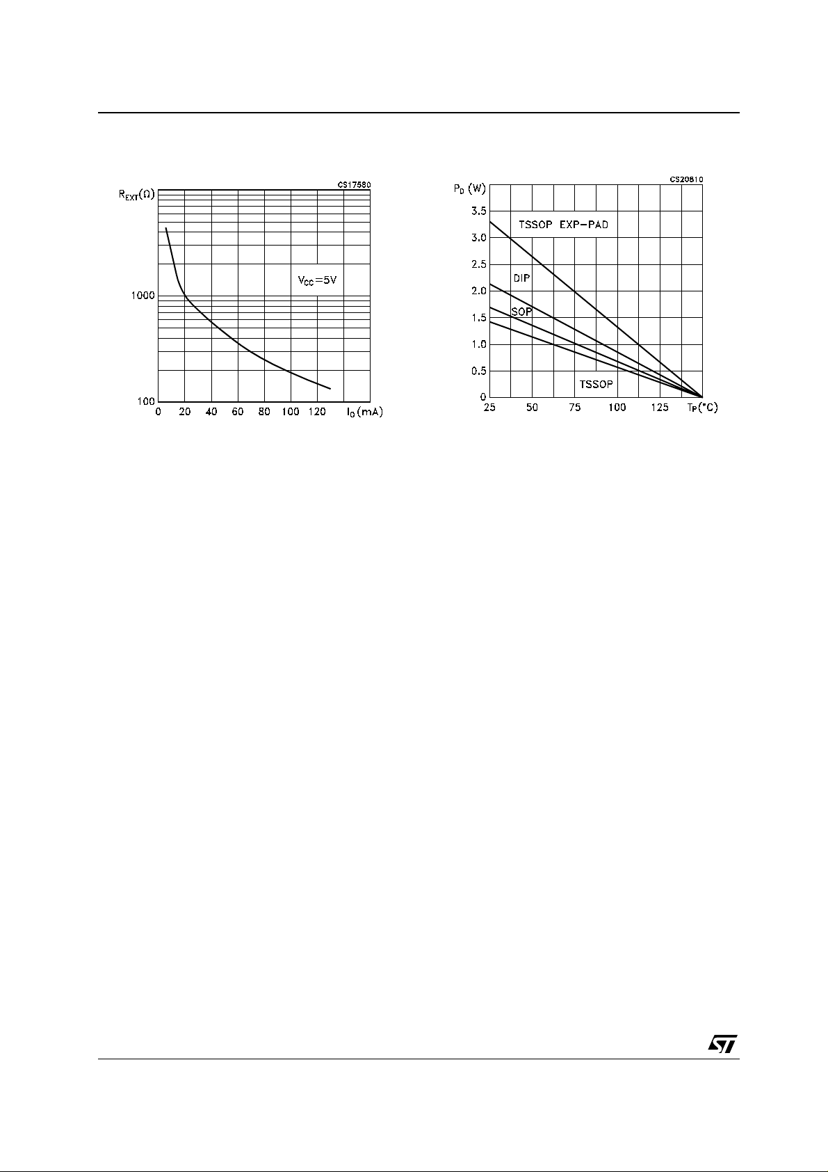
STP16C596
Figure 13: Output Current-R
Resistor
EXT
Figure 14: Power Dissipation vs Temperature
Package
10/18

STP16C596
Plastic DIP-24 (0.25) MECHANICAL DATA
mm. inch
DIM.
MIN. TYP MAX. MIN. TYP. MAX.
A 4.32 0.170
A1 0.38 0.015
A2 3.3 0.130
B 0.41 0.46 0.51 0.016 0.018 0.020
B1 1.40 1.52 1.65 0.055 0.060 0.065
c 0.20 0.25 0.30 0.008 0.010 0.012
D 31.62 31.75 31.88 1.245 1.250 1.255
E 7.62 8.26 0.300 0.325
E1 6.35 6.60 6.86 0.250 0.260 0.270
e 2.54 0.100
E1 7.62 0.300
L 3.18 3.43 0.125 0.135
M 0˚ 15˚ 0˚ 15˚
E
E1
A2
A1
LA
B eB1
D
24
1
13
12
Stand-off
e1
c
.015
0,38
Gage Plane
M
0034965/D
11/18

STP16C596
SO-24 MECHANICAL DATA
DIM.
A 2.35 2.65 0.093 0.104
A1 0.1 0.30 0.004 0.012
B 0.33 0.51 0.013 0.020
C 0.23 0.32 0.009 0.013
D 15.20 15.60 0.598 0.614
E 7.4 7.6 0.291 0.299
e 1.27 0.050
H 10.00 10.65 0.394 0.419
h 0.25 0.75 0.010 0.030
L 0.4 1.27 0.016 0.050
k0° 8° 0° 8°
ddd 0.100 0.004
MIN. TYP MAX. MIN. TYP. MAX.
mm. inch
12/18
0070769C

STP16C596
TSSOP24 EXPOSED PAD MECHANICAL DATA
mm. inch
DIM.
MIN. TYP MAX. MIN. TYP. MAX.
A 1.2 0.047
A1 0.15 0.004 0.006
A2 0.8 1 1.05 0.031 0.039 0.041
b 0.19 0.30 0.007 0.012
c 0.09 0.20 0.004 0.0089
D 7.7 7.8 7.9 0.303 0.307 0.311
D1 2.7 0.106
E 6.2 6.4 6.6 0.244 0.252 0.260
E1 4.3 4.4 4.5 0.169 0.173 0.177
E2 1.5 0.059
e 0.65 0.0256
K0° 8° 0° 8°
L 0.45 0.60 0.75 0.018 0.024 0.030
7100778C
13/18

STP16C596
TSSOP24 MECHANICAL DATA
mm. inch
DIM.
MIN. TYP MAX. MIN. TYP. MAX.
A 1.1 0.043
A1 0.05 0.15 0.002 0.006
A2 0.9 0.035
b 0.19 0.30 0.0075 0.0118
c 0.09 0.20 0.0035 0.0079
D 7.7 7.9 0.303 0.311
E 4.3 4.5 0.169 0.177
e 0.65 BSC 0.0256 BSC
H 6.25 6.5 0.246 0.256
K0° 8° 0° 8°
L 0.50 0.70 0.020 0.028
A2
A
A1
b
e
D
K
c
E
L
H
PIN 1 IDENTIFICATION
14/18
1
7047476B

STP16C596
Tape & Reel SO-24 MECHANICAL DATA
mm. inch
DIM.
MIN. TYP MAX. MIN. TYP. MAX.
A 330 12.992
C 12.8 13.2 0.504 0.519
D 20.2 0.795
N 60 2.362
T 30.4 1.197
Ao 10.8 11.0 0.425 0.433
Bo 15.7 15.9 0.618 0.626
Ko 2.9 3.1 0.114 0.122
Po 3.9 4.1 0.153 0.161
P 11.9 12.1 0.468 0.476
15/18

STP16C596
Tape & Reel TSSOP24 MECHANICAL DATA
mm. inch
DIM.
MIN. TYP MAX. MIN. TYP. MAX.
A 330 12.992
C 12.8 13.2 0.504 0.519
D 20.2 0.795
N 60 2.362
T 22.4 0.882
Ao 6.8 7 0.268 0.276
Bo 8.2 8.4 0.323 0.331
Ko 1.7 1.9 0.067 0.075
Po 3.9 4.1 0.153 0.161
P 11.9 12.1 0.468 0.476
16/18

Table 10: Revision History
Date Revision Description of Changes
06-May-2004 4 Table 6 and Table 7 parameters changed.
03-Aug-2004 5 Figure 14 - pag. 10 is changed.
STP16C596
17/18

STP16C596
Information furnished is believed to be accurate and reliable. However, STMicroelectronics assumes no responsibility for the consequences
of use of s uch inf ormati on nor for a ny infr ing eme nt o f p atent s or o ther ri ghts of third parti es wh ic h m ay r esul t from i ts use. No license is gr an ted
by implication or otherwise under any patent or patent rights of STMicroelectronics. Specifications mentioned in this publication are subject
to change without notice. This publication supersedes and replaces all information previously supplied. STMicroelectronics products are not
authorized for use as critical components in life support devices or systems without express written approval of STMicroelectronics.
The ST logo is a registered trademark of STMicroelectronics
All other names are the property of their respective owners
© 2004 STMicroelectronics - All Rights Reserved
STMicroelectronics group of companies
Australia - Belgium - Brazil - Canada - China - Czech Republic - Finland - France - Germany - Hong Kong - India - Israel - Italy - Japan -
Malaysia - Malta - Morocco - Singapore - Spain - Sweden - Switzerland - United Kingdom - United States of America
www.st.com
18/18
 Loading...