

16-channel LED driver with 16-bit PWM,
8-bit gain and full LED error detection
Features
■ 16 constant current output channels
■ Supply voltage: 3.3 V or 5 V
■ Two PWM selectable counters 12/16-bit of
grayscale
■ Selectable enhanced PWM for ghost effect
reduction
■ Open and short LED detection
■ 8-bit current gain control by means of 256
steps in two selectable ranges
■ Single resistor to set the current from 3 mA to
60 mA
■ Programmable progressive output delay
■ Thermal protection and thermal flag
■ UVLO
■ Schmitt trigger input
■ Selectable 16-bit or 256-bit serial data-in
format
■ Max clock frequency: 30 MHz
■ ESD protection 2.5 kV HBM, 200 V MM
■ Drop-in compatible with STP16CP\S\DP05
series
■ Available in high thermal efficiency TSSOP
exposed pad
Applications
■ Video display LED panels
■ RGB backlighting
■ Special lighting
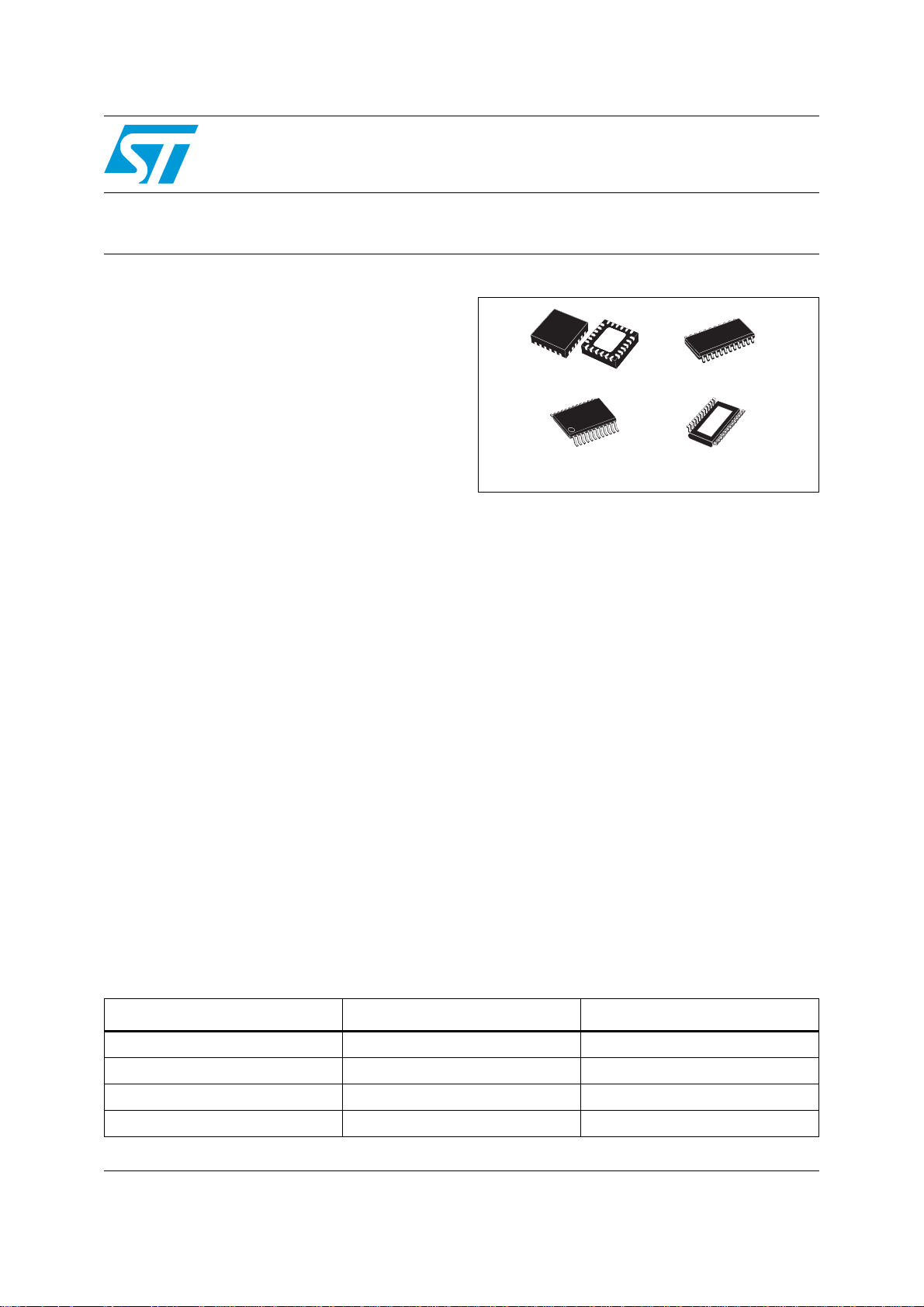
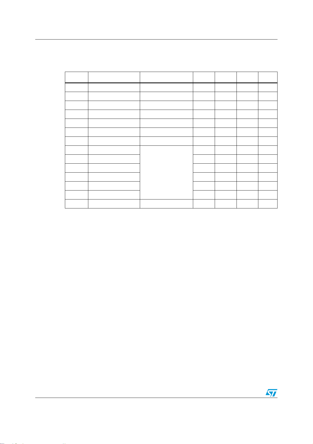
Table 1. Device summary
STP1612PW05
Preliminary data
QFN-24
TSSOP24 TSSOP24
Description
The STP1612PW05 is a 16-channel constant
current sink LED driver. The maximum output
current value for all the 16 channels is set by a
single resistor from 3 mA to 60 mA. The device
features 8-bit gain (256 steps) for global LED
brightness adjustment with two selectable ranges.
This function is accessible via a serial interface.
The device has an individual adjustable PWM
brightness control for each output channel. The
PWM counters are selectable via a serial
interface with 4096 or 65536 steps (12 or 16 bit).
The STP1612PW05 also provides enhanced
pulse-width modulation counting algorithms called
e-PWM to reduce flickering effects (ghost visual
effects) improving the overall image quality. The
device has a dual size 16-bit or 256-bit shift
register. All the control and the shift register read
back data are accessible via serial interface. The
STP1612PW05 has the capability to detect open
and short LED failure and overtemperature,
reporting the status through SPI line. The device
guarantees a 20 V output driving capability,
allowing the user to connect more LEDs in series.
SO-24
exposed pad
STP1612PW05QTR QFN-24 4000 parts per reel
STP1612PW05MTR SO-24 1000 parts per reel
STP1612PW05TTR TSSOP24 2500 parts per reel
STP1612PW05XTTR TSSOP24 exposed pad 2500 parts per reel
February 2011 Doc ID 15819 Rev 5 1/41
This is preliminary information on a new product now in development or undergoing evaluation. Details are subject to
change without notice.
Order code Package Packaging
www.st.com
41

Contents STP1612PW05
Contents
1 Block diagram . . . . . . . . . . . . . . . . . . . . . . . . . . . . . . . . . . . . . . . . . . . . . . 4
2 Summary description . . . . . . . . . . . . . . . . . . . . . . . . . . . . . . . . . . . . . . . . 5
2.1 Pin connection and description . . . . . . . . . . . . . . . . . . . . . . . . . . . . . . . . . 6
3 Electrical ratings . . . . . . . . . . . . . . . . . . . . . . . . . . . . . . . . . . . . . . . . . . . . 7
3.1 Absolute maximum ratings . . . . . . . . . . . . . . . . . . . . . . . . . . . . . . . . . . . . . 7
3.2 Thermal data . . . . . . . . . . . . . . . . . . . . . . . . . . . . . . . . . . . . . . . . . . . . . . . 7
3.3 Recommended operating conditions . . . . . . . . . . . . . . . . . . . . . . . . . . . . . 8
4 Electrical characteristics . . . . . . . . . . . . . . . . . . . . . . . . . . . . . . . . . . . . . 9
5 Timing waveform . . . . . . . . . . . . . . . . . . . . . . . . . . . . . . . . . . . . . . . . . . . 13
6 Principle of operation . . . . . . . . . . . . . . . . . . . . . . . . . . . . . . . . . . . . . . . 14
7 Configuration register . . . . . . . . . . . . . . . . . . . . . . . . . . . . . . . . . . . . . . . 16
8 Grey scales data loading . . . . . . . . . . . . . . . . . . . . . . . . . . . . . . . . . . . . 17
9 Setting the PWM gray scale counter . . . . . . . . . . . . . . . . . . . . . . . . . . . 18
9.1 PWM data synchronization . . . . . . . . . . . . . . . . . . . . . . . . . . . . . . . . . . . . 18
9.2 Synchronization for PWM counting . . . . . . . . . . . . . . . . . . . . . . . . . . . . . 19
10 Error detection conditions . . . . . . . . . . . . . . . . . . . . . . . . . . . . . . . . . . . 20
11 Setting output current . . . . . . . . . . . . . . . . . . . . . . . . . . . . . . . . . . . . . . . 22
12 Constant current . . . . . . . . . . . . . . . . . . . . . . . . . . . . . . . . . . . . . . . . . . . 23
13 Current gain adjustment . . . . . . . . . . . . . . . . . . . . . . . . . . . . . . . . . . . . . 24
14 Delay time of staggered output . . . . . . . . . . . . . . . . . . . . . . . . . . . . . . . 25
15 Thermal protection . . . . . . . . . . . . . . . . . . . . . . . . . . . . . . . . . . . . . . . . . 25
2/41 Doc ID 15819 Rev 5

STP1612PW05 Contents
16 Time-out alert of GCLK disconnection . . . . . . . . . . . . . . . . . . . . . . . . . 26
17 Application information . . . . . . . . . . . . . . . . . . . . . . . . . . . . . . . . . . . . . 27
17.1 LED supply voltage (VLED) . . . . . . . . . . . . . . . . . . . . . . . . . . . . . . . . . . . 27
17.2 Setting grayscale brightness . . . . . . . . . . . . . . . . . . . . . . . . . . . . . . . . . . 29
17.3 Multi device application . . . . . . . . . . . . . . . . . . . . . . . . . . . . . . . . . . . . . . 30
18 Package mechanical data . . . . . . . . . . . . . . . . . . . . . . . . . . . . . . . . . . . . 31
19 Revision history . . . . . . . . . . . . . . . . . . . . . . . . . . . . . . . . . . . . . . . . . . . 40
Doc ID 15819 Rev 5 3/41
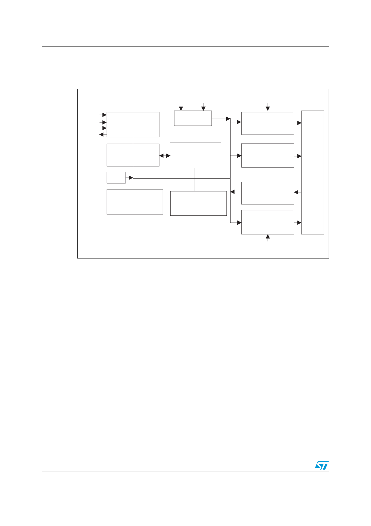
Block diagram STP1612PW05
1 Block diagram
Figure 1. Block diagram
SDI
CLK
LE
SDO
Serial interface
CTRL command
and
CTRL logic
TSD
Shift register
dual size mode
(16 or 256 bit)
GND
VDD
UVLO & POR
16-bit
Configuration
Register
PWM data buffer
(16x16 bit)
R-EXT
Dual range gain
7-bit DAC
Gradual outputs
delay
Open/short
error detection
PWM and e-PWM
12/16 bit counter
and SYNC control
PWCLK
1----------16
Constant current output channels
4/41 Doc ID 15819 Rev 5
STP1612PW05 Summary description
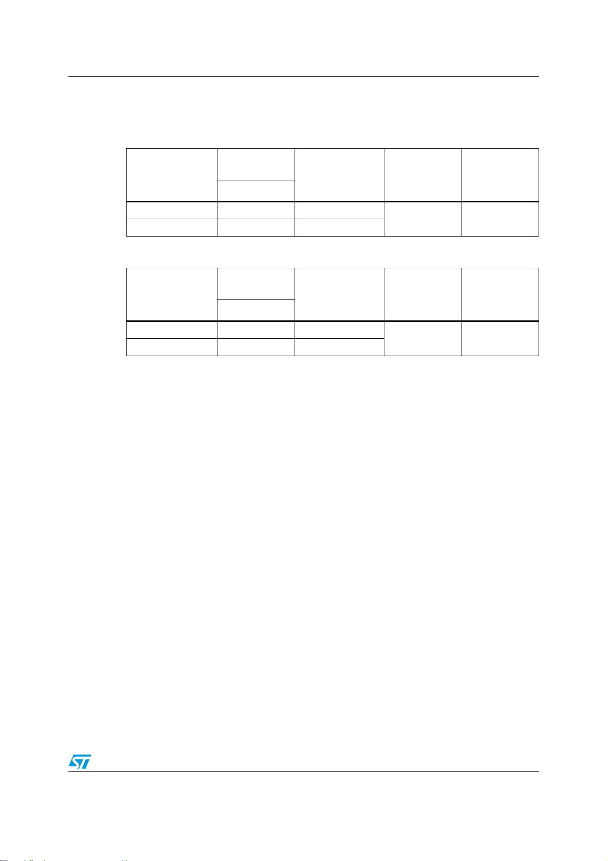
2 Summary description
Table 2. Typical current accuracy at 5 V
Current
Output voltage
accuracy
Between ICs
Output current V
DD
temp.
≥ 1.0 ± 6% 15 to 60
≥ 0,2 ± 6% 3 to 15
Table 3. Typical current accuracy at 3.3 V
Current
Output voltage
accuracy
Output current V
Between ICs
≥ 1.0 ± 6% 15 to 60
≥ 0,3 ± 6% 3 to 15
5 V 25 °C
DD
temp.
3.3 V 25 °C
Doc ID 15819 Rev 5 5/41

Summary description STP1612PW05
2.1 Pin connection and description
Figure 2. Pin connection
SDI
SDI
SDI
R-EXT
R-EXT
R-EXT
VDD
VDD
GND
GND
GND
SDI
SDI
SDI
CLK
CLK
CLK
LE
LE
LE
OUT0
OUT0
OUT0
OUT1
OUT1
OUT1
OUT2
OUT2
OUT2
OUT3
OUT3
OUT3
OUT4
OUT4
OUT4
OUT5
OUT5
OUT5
OUT6
OUT6
OUT6
OUT7
OUT7
OUT7
VDD
VDD
VDD
R-EXT
R-EXT
R-EXT
SDO
SDO
SDO
PWCLK
PWCLK
PWCLK
OUT15
OUT15
OUT15
OUT14
OUT14
OUT14
OUT13
OUT13
OUT13
OUT12
OUT12
OUT12
OUT11
OUT11
OUT11
OUT10
OUT10
OUT10
OUT9
OUT9
OUT9
OUT8
OUT8
OUT8
LE
LE
LE
OUT0
OUT0
OUT0
OUT1
OUT1
OUT1
OUT2
OUT2
OUT2
OUT3
OUT3
OUT3
OUT4
OUT4
OUT4
CLK
CLK
CLK
OUT5
OUT5
OUT5
OUT6
OUT6
OUT6
VDD
OUT7
OUT7
OUT7
SDO
PWCLK
SDO
PWCLK
SDO
PWCLK
OUT15
OUT15
OUT15
OUT14
OUT14
OUT14
OUT13
OUT13
OUT13
OUT12
OUT12
OUT12
OUT11
OUT11
OUT11
OUT10
OUT10
OUT10
GND
GND
GND
OUT9
OUT8
OUT9
OUT8
OUT9
OUT8
Note: The exposed pad should be electrically connected to a metal land electrically isolated or
connected to ground
Table 4. Pin description
Pin n° Symbol Name and function
1 GND Ground terminal
2 SDI Serial data input terminal
3CLK
4 LE Data strobe terminal and controlling command with CLK
5-20 OUT 0-15 Output terminals
21 PWCLK
22 SDO Serial data out terminal
23 R-EXT Input terminal of an external resistor for constant current programing
24 V
DD
Clock input terminal used to shift data on rising edge and carries
command information when LE is asserted.
Gray scale clock terminal.
Reference clock for grey scale PWM counter.
Supply voltage terminal
6/41 Doc ID 15819 Rev 5
STP1612PW05 Electrical ratings
3 Electrical ratings
3.1 Absolute maximum ratings
Stressing the device above the rating listed in the Table 5 may cause permanent damage to
the device. These are stress ratings only and operation of the device at these or any other
conditions above those indicated in the operating sections of this specification is not implied.
Exposure to absolute maximum rating conditions for extended periods may affect device
reliability.
Table 5. Absolute maximum ratings
Symbol Parameter Value Unit
V
V
I
V
I
GND
f
CLK
T
1. Such absolute value is based on the thermal shutdown protection.
Supply voltage 0 to 7 V
DD
Output voltage -0.5 to 20 V
O
Output current 60 mA
O
Input voltage -0.4 to VDD V
I
GND terminal current 1300 mA
Clock frequency 50 MHz
Junction temperature range
J
3.2 Thermal data
Table 6. Thermal data
Symbol Parameter Value Unit
T
J-OPR
T
R
T
STG
thJA
Operating free-air temperature range -40 to +125 °C
A
Operating thermal junction temperature range -40 to +150 °C
Storage temperature range -55 to +150 °C
Thermal resistance junctionambient
(1)
(1)
-40 to + 170 °C
SO-24 42.7 °C/W
TSSOP24 55 °C/W
(2)
TSSOP24
Exposed pad
37.5 °C/W
QFN-24 55 °C/W
1. According to Jedec standard 51-7B
2. The exposed pad should be soldered directly to the PCB to realize the thermal benefits.
Doc ID 15819 Rev 5 7/41
Electrical ratings STP1612PW05
3.3 Recommended operating conditions
Table 7. Recommended operating conditions at 25 °C
Symbol Parameter Test conditions Min. Typ. Max. Unit
V
V
I
OH,SDO
I
OL,SDO
V
V
t
wLAT
t
wCLK
t
wEN
t
SETUP(D)
t
HOLD(D)
t
SETUP(L)
f
CLK
Supply voltage 3.0 - 5.5 V
DD
Output voltage - 20 V
O
Output current, OUTn 3 - 60 mA
I
O
Output current, SDO - +1 mA
Output current, SDO - -1 mA
Input voltage 0.7 V
IH
Input voltage GND - 0.3 V
IL
LE pulse width
DD
20 - ns
-V
CLK pulse width 10 - ns
PWCLK pulse width 20 - ns
VDD = 3.3 V to 5.0 V
Setup time for DATA 5 - ns
Hold time for DATA 5 - ns
Setup time for LATCH 5 - ns
Clock frequency Cascade operation
(1)
-30MHz
V
DD
DD
1. If the device is connected in cascade, it may not be possible achieve the maximum data transfer. Please
considered the timings carefully.
V
8/41 Doc ID 15819 Rev 5
STP1612PW05 Electrical characteristics
4 Electrical characteristics
VDD = 3.3 V ± 10%, VDD = 5 V ± 10%, TA = 25 °C unless otherwise specified
Table 8. Electrical characteristics
Symbol Characteristics Test conditions Min. Typ. Max. Unit
V
O
I
OUT
OH,SDO
I
OL,SDO
V
IH
V
IL
I
OH
V
OL
V
OH
dI
OUT1
dI
OUT1
dI
OUT2
dI
OUT2
%/dV
%/dV
R
IN(down)
I
DD(off) 1
I
DD(off) 2
I
DD(off) 3
Maximum output voltage OUT0 ~ OUT15 20 V
OUT0~OUT115 VO = 2V 3 60
Output
current
SDO -8
mAI
SDO 8
Input voltage “H” level 0.7 * VDD V
Input voltage “L” level GND 0.3 * V
V
DD
V
DD
Output leakage current VO = 20 V 1 µA
I
= +8 mA 0.4 V
Output voltage SDO
Current skew (channel)
Current skew (IC)
Output current vs. output voltage
O
regulation
Output current vs. supply voltage
DD
regulation
OL
IOH = -8 mA V
I
= 3mA, VO = 0.3V,
OUT
= 238.2kΩ
R
EXT
I
= 20mA, VO = 1V,
OUT
R
= 34.7kΩ
EXT
I
= 3mA, VO = 0.3V,
OUT
R
= 238.2kΩ
EXT
I
= 20mA, VO = 1V,
OUT
= 34.7kΩ
R
EXT
VO within 1.0 V and 3.0 V,
R
= 34.7 kΩ @ 20 mA
ext
within 4.5 V and 5.5 V ± 1.0 ± 5.0 % / V
V
DD
- 0.4 V
DD
±1.5 ±3 %
±3 ±6 %
± 0.1 ± 0.5 % / V
Pull-down resistor LE 150 200 250 kΩ
Supply current “Off”
Rext = Open,
OUT0 ~ OUT15 = Off
IO = 3 mA,
~ OUT15 = Off
OUT0
= 60 mA,
I
O
OUT0 ~ OUT15 = Off
811
8.5 11
11 15
mA
I
= 3 mA,
I
DD(on) 1
O
OUT0 ~ OUT15 = On
811.5
Supply current “On”
= 60 mA,
I
I
DD(on) 2
O
~ OUT15 = On
OUT0
11.5 15
Doc ID 15819 Rev 5 9/41
Electrical characteristics STP1612PW05
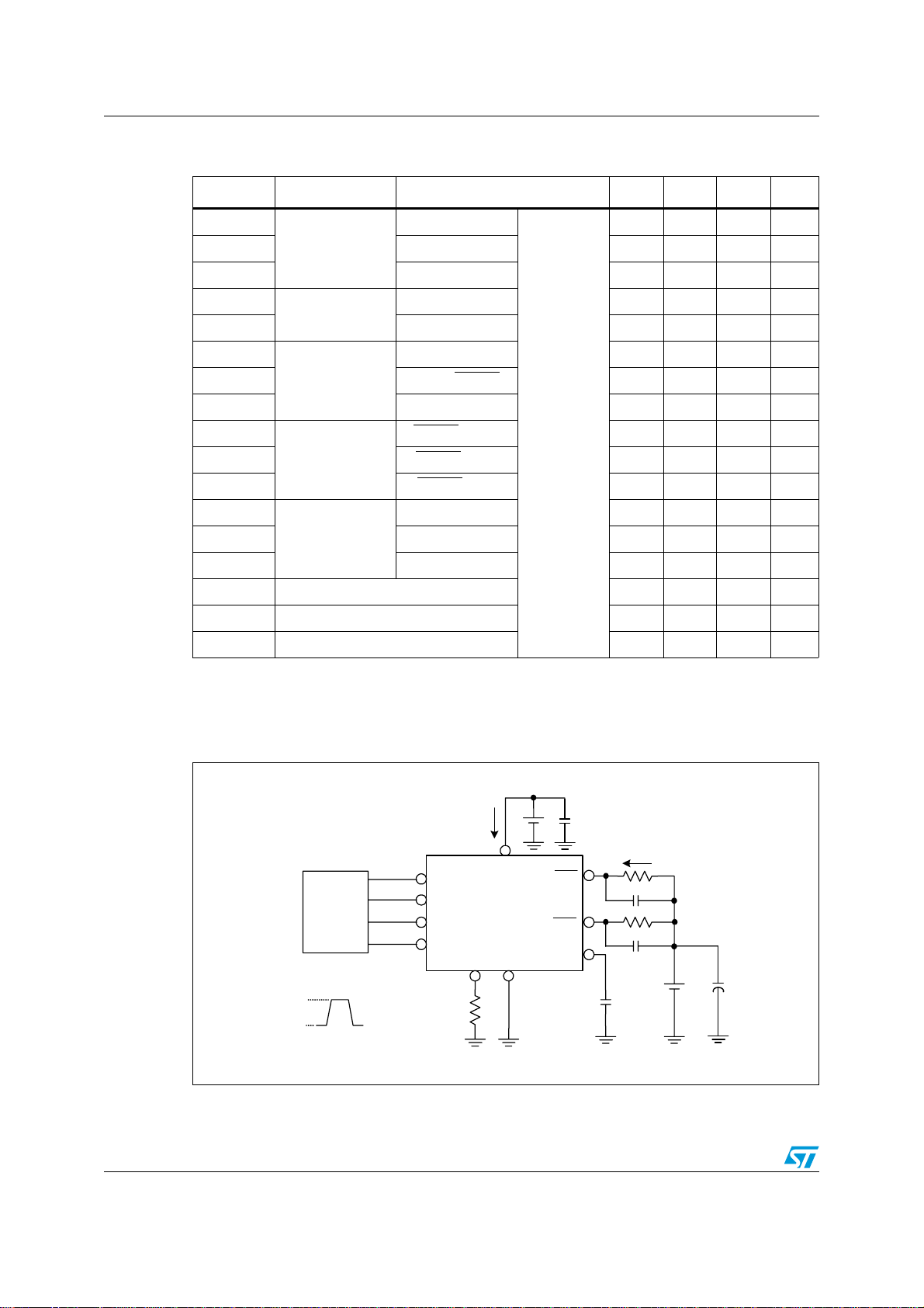
Figure 3. Test circuit for electrical characteristics
VIH=V
DD
VIL=GND
Function
Generator
inputLogic
waveform
VIH,V
DDI
IL
SDI
CLK
LE
PWCLK
R
ext
DDV
GND
EXT-R
V
DD
OUT0
OUT15
.
.
.
SDO
OUT
I
I
OL
I
OH
10/41 Doc ID 15819 Rev 5

STP1612PW05 Electrical characteristics
Table 9. Switching characteristics (VDD = 5.0 V) TA = -40 ~ 125 ° C
Symbol Characteristics Conditions Min. Typ. Max. Unit
t
SU0
t
SU1
t
SU2
t
H0
t
H1
t
PD0
t
PD1
t
PD2
t
DL1
t
DL2
t
DL3
t
w(L)
t
w( CLK)
t
w(PWCLK)
t
ON
t
OFF
t
EDD
Setup time
Hold time
Propagation
PWCLK-OUTn4
delay time
Stagger delay
time
Pulse width
Output rise time of output ports 10 ns
Output fall time of output ports 6 ns
Error detection minimum duration
SDI - CLK ↑
1 ns
LE ↑ – DCLK ↑ 1 ns
LE ↓ – DCLK ↑ 5 ns
CLK ↑ - SDI 3 ns
CLK ↑ - LE ↓ 7 ns
CLK - SDO 30 40 ns
LE – SDO
OUTn4
(2)
+ 1
OUTn4 + 2
OUTn4 +3
LE 5 ns
(1)
(1)
(1)
(1)
V
= 5.0 V
DD
VIH = VDD
VIL = GND
= 460 Ω
R
ext
V
= 4.5 V
LED
RL = 152 Ω
CL = 10 pF
C1 = 100 nF
C2 = 10 µF
= 20 mA
I
O
100 ns
30 40 ns
40 ns
80 ns
120 ns
CLK 20 ns
PWCLK 20 ns
(3)
1µs
1. Refer to the timing waveform, where n = 0, 1, 2, 3.
2. In timing of “read configuration” and “read error status code”, the next CLK rising edge should be t
the falling edge of LE.
3. Refer to Figure 5 on page 13.
PD2
after
Doc ID 15819 Rev 5 11/41
Electrical characteristics STP1612PW05
Table 10. Switching characteristics (V
= 3.3 V)
DD
Symbol Characteristics Conditions Min. Typ. M ax. Unit
t
SU0
t
SU1
t
SU2
t
H0
t
H1
t
PD0
t
PD1
t
PD2
t
DL1
t
DL2
t
DL3
t
w(L)
t
w(CLK)
t
w(PWCLK)
t
ON
t
OFF
t
DEC
Setup time
Hold time
Propagation delay
PWCLK-OUTn4
time
Stagger delay
time
Pulse width
Output rise time of output ports 11.6 ns
Output fall time of output ports 7 ns
Error detection duration 0.5 1 µs
1. Refer to the timing waveform Figure 4, where n = 0, 1, 2, 3.
2. In timing of “read configuration” and “read error status code”, the next CLK rising edge should be t
the falling edge of LE.
SDI - DCLK ↑
1 ns
LE ↑ – DCLK ↑ 1 ns
LE ↓ – DCLK ↑ 5 ns
CLK ↑ - SDI 3 ns
CLK ↑ - LE ↓ 7 ns
CLK - SDO 45 40 ns
LE – SDO
+ 1
OUTn4
OUTn4 + 2
OUTn4 +3
LE 5 ns
(1)
(2)
(1)
(1)
(1)
VDD = 3.3 V
VIH = VDD
= GND
V
IL
R
= 460 Ω
ext
= 4.5 V
V
LED
RL = 152 Ω
CL = 10 pF
C1 = 100 nF
C2 = 10 µF
120 ns
45 40 ns
40 ns
80 ns
120 ns
CLK 20 ns
PWCLK 20 ns
after
PD2
Figure 4. Test circuit for switching characteristics
VIH,V
IL
SDI
Function
Generator
inputLogic
VIH=V
DD
VIL=GND
12/41 Doc ID 15819 Rev 5
CLK
LE
PWCLK
V
DDV
GND
DD
OUT0
OUT15
SDO
1
C
OUT
I
.
.
.
R
L
C
L
R
L
C
L
V
C
LED waveform
C
L
2
DDI
EXT-R
R
ext
STP1612PW05 Timing waveform
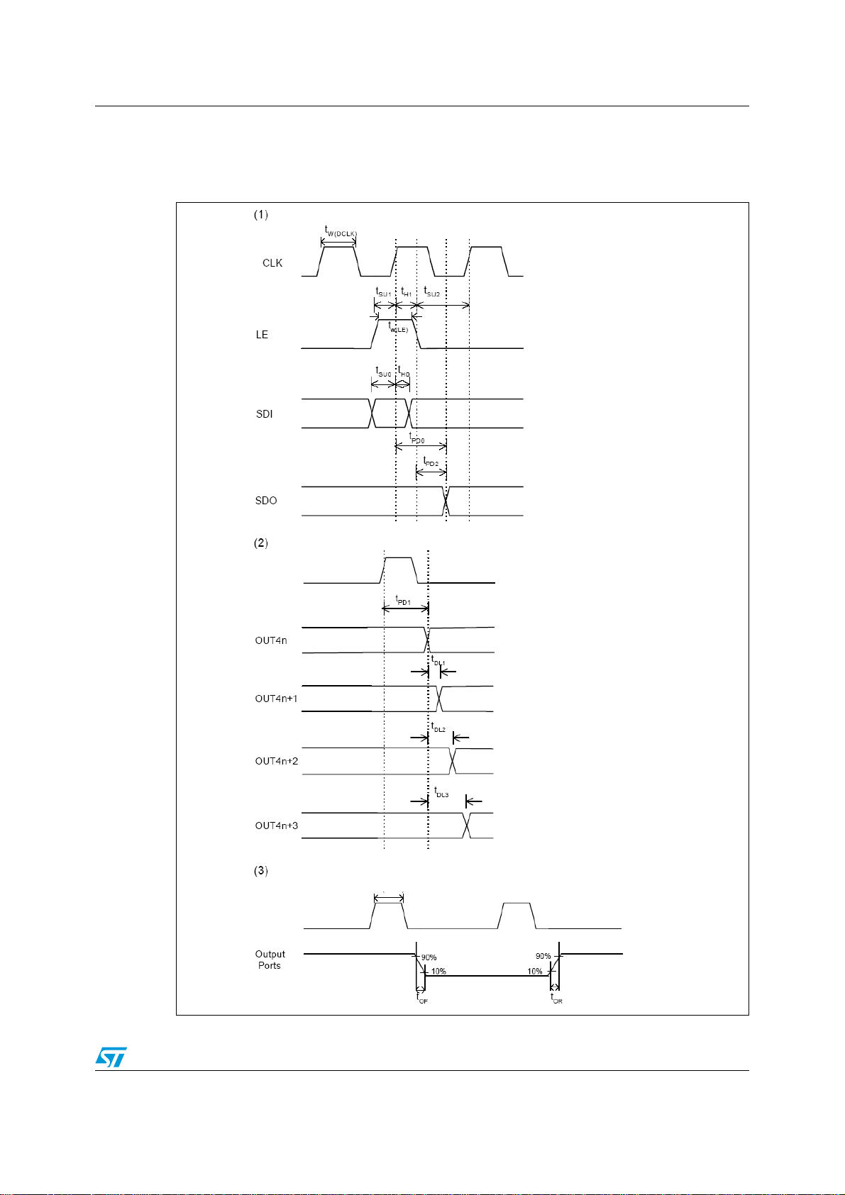
5 Timing waveform
Figure 5. Timing waveform
PWCLK
PWCLK
PWCLK
Doc ID 15819 Rev 5 13/41

Principle of operation STP1612PW05
6 Principle of operation
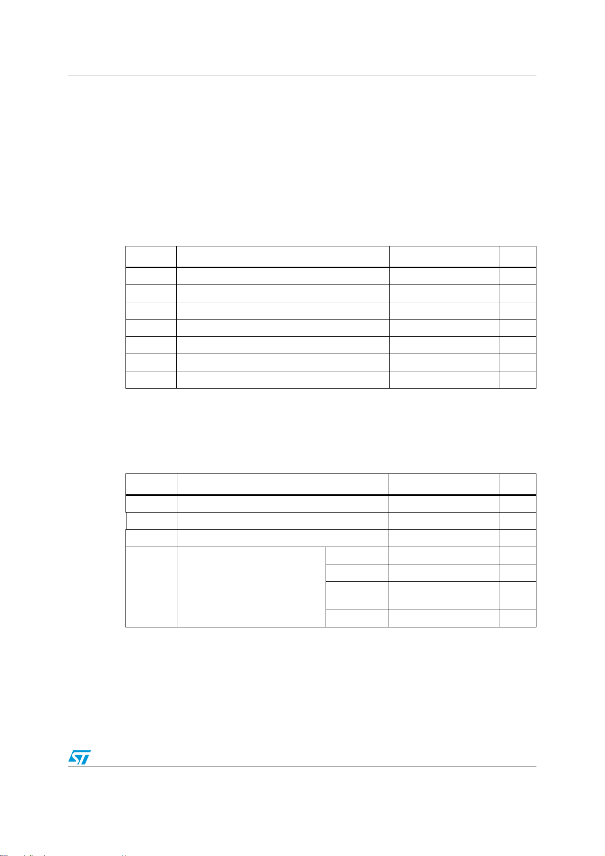
Table 11. Control command
Signals combination Description
Number of CLK
Command name LE
Data latch High 1 Serial data are transferred to the buffers
Global latch High 2 or 3 Buffer data are transferred to the comparators
Read configuration High 4 or 5
rising edge when
LE is asserted
The action after a falling edge of LE
Move out “configuration register” to the shift
register
Enable “error
detection”
Read “error status
code”
High 6 or 7 Detect the status of each output’s LED
High 8 or 9
Write configuration High 10 or 11
Reset to 16-bit shift
register length
High 12 or 13 Set to 16-bit the shift register length
Move out “error status code” of 16 outputs to
the shift registers
Serial data are transferred to the
“configuration register”
14/41 Doc ID 15819 Rev 5

STP1612PW05 Principle of operation
Figure 6. Timing diagram
$ATA,ATCH
#,+
...
,%
3$)
3$/
-3"
$
$ $ $
$
$ $ $ $ $ $ $
$
0REVIOUS$ATA
$$
$
.EXT$ATA
$ $ $
'LOBAL,ATCH
#,+
...
,%
3$)
3$/
-3"
$
$ $ $
$
$ $ $ $ $ $ $
$
0REVIOUS$ATA
$$
$
.EXT$ATA
$ $ $
2EAD#ONFIGURATION
#,+
...
....
..
,%
3$/
0REVIOUS$ATA
&
$ #
%
!
"
7RITE#ONFIGURATION
#,+
,%
3$)
..
& %
#
$
" !
.
.EXT$ATA
%
3$/
0REVIOUS$ATA
&
$
Doc ID 15819 Rev 5 15/41

Configuration register STP1612PW05
7 Configuration register
Table 12. Configuration register
Bit Attribute Definition Value Function
15 Read/Write
14 Read
13 Read/Write
12-11 Read/Write
Shift register
length
Thermal error
flag
PWM counter
(12/16 bit)
PWM counting
mode
selection
0 16 bit shift register
1 256 bit shift register
0 Temperature OK
1 Over temperature (>150°C typ.)
0 12 bit Grayscale PWM counter
1 16 bit Grayscale PWM counter
(1)
00
01
10
64 times of MSB
(1)
of LSB
6-bit PWM
16 times of MSB 6-bit PWM counting by 1/4
PWCLK plus once of LSB 6-bit PWM counting
4 times of MSB 6-bit PWM counting by 1/16
PWCLK plus once of LSB 6-bit PWM counting
6-bit PWM counting plus once
11 PWM counting
10 Read/Write
9-2 Read/Write
PWM data
synchronizatio
n mode
Current gain
adjustment
0 Auto-synchronization
1 Manual synchronization
00000000
11111111
Adjust the current value set by R-EXT over 256
~
steps
Default
value
0
0
0
11
1
8b 10101011
Thermal
1 Read/Write
Shutdown
function
Time-out alert
0 Read/Write
for PWCLK
disconnection
1. Please refer to “setting the PWM counting mode” section.
2. Please refer to “TSD” thermal error flag and thermal shutdown “section.
3. Please refer to “time-out alert of PWCLK disconnection” section.
0 Disable
Enable
1
overcomes 150°C)
0 Enable
1 Disable
16/41 Doc ID 15819 Rev 5
(2)
(output channels OFF if temperature
(3)
0
0

STP1612PW05 Grey scales data loading
8 Grey scales data loading
The STP1612PW05 is able to manage a gray-scale depth of 12 or 16 bits for each output,
exploiting an e-PWM algorithm.
The bit D of the configuration register is used to select the grey-scale loading. Its value can
be set to “0” for 12 bits or “1” for 16 bits. By default, D is set to “0”.
Loading of the data is performed through the serial input on a dedicated buffer and two
different methods can be used.
With both methods, the first incoming data packet is relative to the output 15; the following
packet is relative to the output 14 and so on up to the output 0.
If F=”0”, when a data packet has been loaded, the latch signal (LE) must become active for
one CLK cycle (data latch). When the last data packet, relative to the output 0, has been
loaded, the latch signal must be active for two CLK cycles (global latch) and all the data will
be transferred to the e-PWM registers starting from the MSB.
If F=”1” all data packets (12 or 16 bits x16) are loaded and then the global latch signal must
be active and all the data will be transferred to the e-PWM registers starting from the MSB.
Figure 7. Full timing for data loading
Doc ID 15819 Rev 5 17/41

Setting the PWM gray scale counter STP1612PW05
9 Setting the PWM gray scale counter
STP1612PW05 provides a 12-bit or 16-bit PWM color depth. Each serial data input will be
implemented according to the e-PWM algorithm.
9.1 PWM data synchronization
STP1612PW05 defines the different counting algorithms that support e-PWM, technology,
(scrambled PWM). With e-PWM, the total PWM cycles can be broken down into MSB (most
significant bits) and LSB (least significant bits) of gray scale cycles, and the MSB
information can be dithered across many refresh cycles to achieve overall same high bit
resolution. STP1612PW05 also allows changing different counting algorithms and provides
the best output linearity when there are fewer transitions of output.
Figure 8. 12-bit e-PWM operation example
PWCLK
PWCLK
PWCLK
PWCLK
PWCLK
18/41 Doc ID 15819 Rev 5

STP1612PW05 Setting the PWM gray scale counter
9.2 Synchronization for PWM counting
The data synchronization between the incoming data flow and the output channels is
managed through the bit A within the configuration register.
If the bit A is set to “0” the device performs itself the data synchronization: when all the new
data are loaded with a “global latch”, the device wait until all the PWM counter completes
the counting cycle before updating them with the new data, at the next CLK rising edge.
Conversely, if bit A is set to “1” (default), the data synchronization is not performed by the
device and is managed by the microcontroller, which has to take care of the data and
signals. If this is not done, there might be artefacts on the output image.
Figure 9. Synchronization for PWM counting
CLK
PWCLK
Figure 10. Without synchronization for PWM counting
CLK
PWCLK
Doc ID 15819 Rev 5 19/41

Error detection conditions STP1612PW05
10 Error detection conditions
The STP1612PW05 can detect open channels (OD) and LED short-circuits (SD).
The detection circuitry performs open- and short-circuit detection simultaneously and needs
that all channels must be on. However the short test duration (0.5 µs typ) does not impact
the image quality.
According to Table 11, the command “Enable Error Detection” starts the diagnostic process.
After 0.5 µs (typ) the faults detection has already been carried out and, through the
command “Read Error Status Code”, the status is available on the serial output (SDO).
A bit set to "1" in the Error Status Code represents a channel considered good, whereas a
"0" represents a failed output (open/short).
Figure 11 describes the error detection process.
Figure 11. Error detection process
“Read Error Status Code”
“Enable Error Detection”
“Enable Error Detection”
command
command
“Read Error Status Code”
command
command
CLK
CLK
LE
LE
from SDI
SDO
SDO
from SDI
don’t care don’t care
don’t care don’t care
detection of faulty
detection of faulty
channels (typ 0.5µs)
channels (typ 0.5µs)
The Table 13 and Figure 12 explains the fault conditions detected by the diagnostic circuitry
and how the detection is performed.
Table 13. Detection conditions (V
SW-1 or
SW-3b
SW-2 or
SW-3a
Open line or output short to GND
detected
Short on LED or short to V-LED
detected
= 3.3 to 5 V temp. range -40 to 125 °C)
DD
Note: Where: IO = the output current programmed by the R
current in detection mode
EXT
==> I
==> V
, I
ODEC
ERROR STATUS CODE
ERROR STATUS CODE
≤ 0.5 x I
ODEC
≥ 2.3 V
O
O
= the detected output
20/41 Doc ID 15819 Rev 5

STP1612PW05 Error detection conditions
Figure 12. Detection circuit
16
STP1612PW05
Doc ID 15819 Rev 5 21/41

Setting output current STP1612PW05
11 Setting output current
The output current (I
) is set by an external resistor, R
OUT
ext
.
It is calculated from the equation:
V
Whereas R
and V
R-EXT
R-EXT
= 1.24 x G; I
is the resistance of the external resistor connected to R-EXT terminal
ext
OUT
= (V
R-EXT/Rext
) x 560
is its voltage. G is the digital current gain, which is set by the bit9 – bit2 of the
configuration register. The default value of G is 1. For your information, the output current is
about 20 mA when R
= 34.70 kΩ and 10 mA when R
ext
= 69.6 kΩ if G is set to
ext
default value 1. The formula and setting for G are described in next section.
Figure 13. Rext vs output current
275
250
225
200
175
150
125
100
Rex t (kO hm)
75
50
25
0
3 5 10 20 30 50 60 80
Iout (m A)
Table 14. Rext vs output current
Iout (mA) Rext (kΩ)
3 238.2
5 142.2
10 69.6
20 34.70
30 22.94
50 13.72
60 11.40
80 8.63
1. T
= 25 °C, Vdd = 3.3 V; 5.0 V, V
A
Led
(1)
= 3.0 V, V
= 1.5 V, HC = 0101011 (default)
drop
22/41 Doc ID 15819 Rev 5

STP1612PW05 Constant current
12 Constant current
The STP1612PW05 assures nearly no variation in current both from channel to channel and
from IC to IC.
The typical variation of the current between channels of the same IC is ±1.5%, whereas the
variation between ICs is around ±3%.
Moreover the current characteristic of the output stage is flat (see Figure 14 and Figure 15).
This contributes to keep the current constant regardless of the variation of the LEDs forward
voltage (V
) and consequently guarantees uniformity of brightness.
F
Figure 14. I
Figure 15. I
vs voltage drop across current generators (3.3 V supply voltage)
OUT
vs voltage drop across current generators (5 V supply voltage)
OUT
The typical characteristics in Figure 14 and Figure 15 also show the minimum voltage drop
required to assure that the current generators regulate the desired current.
This must be taken into account when choosing the suitable value of the LED supply voltage
(see dedicated section).
Doc ID 15819 Rev 5 23/41

Current gain adjustment STP1612PW05
13 Current gain adjustment
Figure 16. Gain vs DA6 - DA0
The bit 9 to bit 2 of the configuration register set the gain of output current, i.e., G. Being 8bit in total, ranging from 8’b00000000 to 8’b11111111, these bits allow the user to set the
output current gain up to 256 levels. These bits can be further defined in the configuration
register as follows:
Configuration register
MSB LSB
FEDCBA9876543210
------HCDA6DA5DA4DA3DA2DA1DA0--
1. Bit 9 is HC bit. The setting is in the low current range when HC=0, and in the high
current range when HC=1.
2. Bit 8 to bit 2 are DA6 ~ DA0.
The relationship between these bits and current gain G is:
HC = 1, D = (256G-128)/3
HC = 0, D = (1024G-128)/3
and D in the above decimal numeration can be converted to its equivalent in binary form by
the following equation:
D = DA6x2
6
+ DA5x25 + DA4x24 + DA3x23 + DA2x22 + DA1x21 + DA0x2
0
In other words, these bits can be looked as a floating number with 1-bit exponent HC and 7bit mantissa DA6~DA0.
24/41 Doc ID 15819 Rev 5

STP1612PW05 Delay time of staggered output
For example,
HC = 1, G = 1.25, D = (256x1.25-128)/3 = 64
the D in binary form would be:
D = 64 = 1x2
6
+0x25+0x24+0x23+0x22+0x21+0x2
0
The bit 9 to bit 2 of the configuration register are set to 8’b1100,0000.
14 Delay time of staggered output
This feature prevents large inrush current from the power line and reduces the bypass
capacitors.
The outputs are organized in four groups OUT4n, OUT4n+1, OUTn4+2, OUT4n+3 and each
group has 40 ns delay between the previous one.
E.g.: OUT4n has no delay, OUTn4+1 has 40ns delay, OUTn4+2 has 80ns delay, OUTn4+3
has 120 ns delay.
15 Thermal protection
Thermal flag provides an indication about the status of the junction temperature. When the
junction temperature reaches 150 °C the bit E of the configuration register is set to “1”,
signaling dangerous operating condition. This flag is useful when thermal shutdown function
is disabled.
The thermal shutdown function, if activated by configuration register (bit “1” set to 1), turnsoff all output channels if the junction exceeds 150 °C. As soon as the junction temperature is
below 140 °C the outputs channels will be turned ON. In thermal shutdown mode, the digital
core is active and data flow is guaranteed.
Doc ID 15819 Rev 5 25/41

Time-out alert of GCLK disconnection STP1612PW05
16 Time-out alert of GCLK disconnection
When the PWCLK signal is disconnected for around 1 second, all output ports will be turned
off automatically. This function will protect the LED display system from staying ON
indefinitely and prevent excessive current from damaging the power system. The default is
set to ‘enable” when bit “0” of the Configuration Register is 0. When the PWCLK is active
again and new serial data are moved in, the driver resumes to work after resetting the
internal counters and comparators.
Figure 17. Time-out alert application scheme
PWCLK
500K
STP1612PW05 STP1612PW05 STP1612PW05 STP1612PW05
26/41 Doc ID 15819 Rev 5

STP1612PW05 Application information
+
(
)
17 Application information
17.1 LED supply voltage (VLED)
The choice of the LED supply voltage (VLED) must be carried out considering several
parameters:
● The voltage drop across current generators (V
the desired current (see Figure 14 and Figure 15)
● The maximum LED forward voltage (V
● The maximum power that can be dissipated by the package under the application
F, m a x
ambient conditions
● The accuracy of the supply voltage itself (VLED can vary in a range and the minimum
value should be considered)
Therefore the minimum LED supply voltage can be calculated as:
), which must be enough to guarantee
O
)
=
The LED supply voltage should be higher than V
VVV
max,Ftyp,Omin,LED
(to consider any fluctuation of the
LED,min
involved parameters) but not too high in order to keep low the power dissipation:
16
DIVIVP ⋅⋅+⋅=
i
CHii,ODDDDD
1i
where D
is the duty cycle of the channel i.
i
∑
=
In particular the power dissipation should be kept below the maximum power dissipation,
defined as:
TT
−
P
=
max,D
aj
θ
ja
To summarize, the choice of the proper power supply must be a trade-off between the
correct value that assures the desired LED current and low power dissipation.
In RGB application, there can be a significant variability of the LEDs forward voltage (e.g.
red LEDs have a lower forward voltage compared to green and blue ones).
In this case the supply voltage must be chosen high enough to correctly switch on the LEDs
with the highest forward voltage (green or blue). However this supply voltage is higher than
the voltage required by red LEDs. Thus, the excess of voltage in the lines with red LEDs
drops on the current generators, bringing to an increase of the power dissipation and loss of
efficiency.
Moreover the extra-voltage across the red LEDs driving generators could cause an
erroneous shorted LED condition detection.
Doc ID 15819 Rev 5 27/41

Application information STP1612PW05
To avoid these drawbacks, two different approaches are possible:
● Figure 18 shows an application with only one voltage rail (VLED). A resistor in series to
each red LEDs is added. In this way, the voltage excess drops across the resistor
instead of dropping across the current generators. This solution implies a significant
reduction of the power dissipated by the chip. However the total power dissipation does
not change and a remarkable part of the power is still wasted on the series resistor.
This not only affects the efficiency, but also raises the cost of the system due to the need to
dissipate the generated heat.
Figure 18. Solution with single supply voltage
VLED
VLED
VLED
VLED
VLED
VLED
5V
5V
to SDI of
to SDI of
to SDI of
to SDI of
to SDI of
to SDI of
the next
the next
the next
the next
the next
the next
device
device
device
device
device
device
SDO
SDO
SDO
SDO
SDO
SDO
V
V
V
V
V
V
V
V
V
V
V
V
V
V
V
V
V
V
Rred
Rred
Rred
Rred
Rred
Rred
Rred
Rred
Rred
Rred
Rred
Rred
Rred
Rred
Rred
Rred
Rred
Rred
OUT0
OUT0
OUT0
OUT0
OUT0
OUT0
OUT0
OUT0
OUT0
OUT0
OUT0
OUT0
OUT0
OUT0
OUT0
OUT0
OUT0
OUT0
R
R
R
R
R
R
R
R
R
R
R
R
R
R
R
R
R
R
red
red
red
red
red
red
red
red
red
red
red
red
red
red
red
red
red
red
……
……
……
……
……
……
……
……
……
……
……
……
……
……
……
……
……
……
V
V
V
V
V
V
V
V
V
V
V
V
V
V
V
V
V
V
F,red
F,red
F,red
F,red
F,red
F,red
F,red
F,red
F,red
F,red
F,red
F,red
F,red
F,red
F,red
F,red
F,red
F,red
V
V
V
V
V
V
V
V
V
V
V
V
V
V
V
V
V
V
O,red
O,red
O,red
O,red
O,red
O,red
O,red
O,red
O,red
O,red
O,red
O,red
O,red
O,red
O,red
O,red
O,red
O,red
STP1612PW05
STP1612PW05
STP1612PW05
STP1612PW05
STP1612PW05
STP1612PW05
STP1612PW05
STP1612PW05
STP1612PW05
STP1612PW05
STP1612PW05
STP1612PW05
STP1612PW05
STP1612PW05
STP1612PW05
STP1612PW05
STP1612PW05
STP1612PW05
……
……
……
……
……
……
OUT15
OUT15
OUT15
OUT15
OUT15
OUT15
OUT15
OUT15
OUT15
OUT15
OUT15
OUT15
OUT15
OUT15
OUT15
OUT15
OUT15
OUT15
to SDI of
to SDI of
to SDI of
to SDI of
to SDI of
to SDI of
the next
the next
the next
the next
the next
the next
device
device
device
device
device
device
SDO
SDO
SDO
SDO
SDO
SDO
OUT0
OUT0
OUT0
OUT0
OUT0
OUT0
OUT0
OUT0
OUT0
OUT0
OUT0
OUT0
OUT0
OUT0
OUT0
OUT0
OUT0
OUT0
……
……
……
……
……
……
……
……
……
……
……
……
……
……
……
……
……
……
V
V
V
V
V
V
V
V
V
V
V
V
V
V
V
V
V
V
F,green
F,green
F,green
F,green
F,green
F,green
F,green
F,green
F,green
F,green
F,green
F,green
F,green
F,green
F,green
F,green
F,green
F,green
V
V
V
V
V
V
V
V
V
V
V
V
V
V
V
V
V
V
O,green
O,green
O,green
O,green
O,green
O,green
O,green
O,green
O,green
O,green
O,green
O,green
O,green
O,green
O,green
O,green
O,green
O,green
STP1612PW05
STP1612PW05
STP1612PW05
STP1612PW05
STP1612PW05
STP1612PW05
STP1612PW05
STP1612PW05
STP1612PW05
STP1612PW05
STP1612PW05
STP1612PW05
STP1612PW05
STP1612PW05
STP1612PW05
STP1612PW05
STP1612PW05
STP1612PW05
……
……
……
……
……
……
OUT15
OUT15
OUT15
OUT15
OUT15
OUT15
OUT15
OUT15
OUT15
OUT15
OUT15
OUT15
OUT15
OUT15
OUT15
OUT15
OUT15
OUT15
to SDI of
to SDI of
to SDI of
to SDI of
to SDI of
to SDI of
the next
the next
the next
the next
the next
the next
device
device
device
device
device
device
SDO
SDO
SDO
SDO
SDO
SDO
OUT0
OUT0
OUT0
OUT0
OUT0
OUT0
OUT0
OUT0
OUT0
OUT0
OUT0
OUT0
OUT0
OUT0
OUT0
OUT0
OUT0
OUT0
……
……
……
……
……
……
……
……
……
……
……
……
……
……
……
……
……
……
V
V
V
V
V
V
V
V
V
V
V
V
V
V
V
V
V
V
F,blue
F,blue
F,blue
F,blue
F,blue
F,blue
F,blue
F,blue
F,blue
F,blue
F,blue
F,blue
F,blue
F,blue
F,blue
F,blue
F,blue
F,blue
V
V
V
V
V
V
V
V
V
V
V
V
V
V
V
V
V
V
O,blue
O,blue
O,blue
O,blue
O,blue
O,blue
O,blue
O,blue
O,blue
O,blue
O,blue
O,blue
O,blue
O,blue
O,blue
O,blue
O,blue
O,blue
STP1612PW05
STP1612PW05
STP1612PW05
STP1612PW05
STP1612PW05
STP1612PW05
STP1612PW05
STP1612PW05
STP1612PW05
STP1612PW05
STP1612PW05
STP1612PW05
STP1612PW05
STP1612PW05
STP1612PW05
STP1612PW05
STP1612PW05
STP1612PW05
……
……
……
……
……
……
OUT15
OUT15
OUT15
OUT15
OUT15
OUT15
OUT15
OUT15
OUT15
OUT15
OUT15
OUT15
OUT15
OUT15
OUT15
OUT15
OUT15
OUT15
V
V
V
V
V
V
V
V
V
V
V
V
V
V
V
V
V
V
R
R
R
R
R
R
R
R
R
R
R
R
R
R
R
R
R
R
Rred
Rred
Rred
Rred
Rred
Rred
Rred
Rred
Rred
Rred
Rred
Rred
Rred
Rred
Rred
Rred
Rred
Rred
red
red
red
red
red
red
red
red
red
red
red
red
red
red
red
red
red
red
……
……
……
……
……
……
……
……
……
……
……
……
……
……
……
……
……
from SDO of
from SDO of
from SDO of
from SDO of
from SDO of
from SDO of
the previous
the previous
the previous
the previous
the previous
the previous
device
device
device
device
device
device
……
V
V
V
V
V
V
V
V
V
V
V
V
V
V
V
V
V
V
F,red
F,red
F,red
F,red
F,red
F,red
F,red
F,red
F,red
F,red
F,red
F,red
F,red
F,red
F,red
F,red
F,red
F,red
OUT15
OUT15
OUT15
OUT15
OUT15
OUT15
OUT15
OUT15
OUT15
OUT15
OUT15
OUT15
OUT15
OUT15
OUT15
OUT15
OUT15
V
V
V
V
V
V
V
V
V
V
V
V
V
V
V
V
V
V
O,red
O,red
O,red
O,red
O,red
O,red
O,red
O,red
O,red
O,red
O,red
O,red
O,red
O,red
O,red
O,red
O,red
O,red
STP1612PW05
STP1612PW05
STP1612PW05
STP1612PW05
STP1612PW05
STP1612PW05
STP1612PW05
STP1612PW05
STP1612PW05
STP1612PW05
STP1612PW05
STP1612PW05
STP1612PW05
STP1612PW05
STP1612PW05
STP1612PW05
STP1612PW05
STP1612PW05
OUT15
V
V
V
V
V
V
V
V
V
V
V
V
V
V
V
V
V
V
O,green
O,green
O,green
O,green
O,green
O,green
O,green
O,green
O,green
O,blue
O,blue
O,blue
O,blue
O,blue
O,blue
O,blue
O,blue
O,blue
SDI
SDI
SDI
SDI
SDI
SDI
from SDO of
from SDO of
from SDO of
from SDO of
from SDO of
from SDO of
the previous
the previous
the previous
the previous
the previous
the previous
device
device
device
device
device
device
OUT0
OUT0
OUT0
OUT0
OUT0
OUT0
OUT0
OUT0
OUT0
OUT0
OUT0
OUT0
OUT0
OUT0
OUT0
OUT0
OUT0
OUT0
SDI
SDI
SDI
SDI
SDI
SDI
OUT0
OUT0
OUT0
OUT0
OUT0
OUT0
OUT0
OUT0
OUT0
OUT0
OUT0
OUT0
OUT0
OUT0
OUT0
OUT0
OUT0
OUT0
V
V
V
V
V
V
V
V
V
……
……
……
……
……
……
……
……
……
……
……
……
……
……
……
……
……
……
V
V
V
V
V
V
V
V
V
V
V
V
V
V
V
V
V
V
F,green
F,green
F,green
F,green
F,green
F,green
F,green
F,green
F,green
F,green
F,green
F,green
F,green
F,green
F,green
F,green
F,green
F,green
V
V
V
V
V
V
V
V
V
V
V
V
V
V
V
V
V
V
O,green
O,green
O,green
O,green
O,green
O,green
O,green
O,green
O,green
O,green
O,green
O,green
O,green
O,green
O,green
O,green
O,green
O,green
STP1612PW05
STP1612PW05
STP1612PW05
STP1612PW05
STP1612PW05
STP1612PW05
STP1612PW05
STP1612PW05
STP1612PW05
STP1612PW05
STP1612PW05
STP1612PW05
STP1612PW05
STP1612PW05
STP1612PW05
STP1612PW05
STP1612PW05
STP1612PW05
VLED
VLED
VLED
VLED
VLED
VLED
VLED
VLED
VLED
F,green
F,green
F,green
F,green
F,green
F,green
F,green
F,green
F,green
V
V
V
V
V
V
V
V
V
F,red
F,red
F,red
F,red
F,red
F,red
F,red
F,red
F,red
OUT15
OUT15
OUT15
OUT15
OUT15
OUT15
OUT15
OUT15
OUT15
OUT15
OUT15
OUT15
OUT15
OUT15
OUT15
OUT15
OUT15
OUT15
V
V
V
V
V
V
V
V
V
F,blue
F,blue
F,blue
F,blue
F,blue
F,blue
F,blue
F,blue
F,blue
SDI
SDI
SDI
SDI
SDI
SDI
from SDO of
from SDO of
from SDO of
from SDO of
from SDO of
from SDO of
the previous
the previous
the previous
the previous
the previous
the previous
device
device
device
device
device
device
OUT0
OUT0
OUT0
OUT0
OUT0
OUT0
OUT0
OUT0
OUT0
OUT0
OUT0
OUT0
OUT0
OUT0
OUT0
OUT0
OUT0
OUT0
V
V
V
V
V
V
V
V
V
O,red
O,red
O,red
O,red
O,red
O,red
O,red
O,red
O,red
……
……
……
……
……
……
……
……
……
……
……
……
……
……
……
……
……
……
V
V
V
V
V
V
V
V
V
V
V
V
V
V
V
V
V
V
F,blue
F,blue
F,blue
F,blue
F,blue
F,blue
F,blue
F,blue
F,blue
F,blue
F,blue
F,blue
F,blue
F,blue
F,blue
F,blue
F,blue
F,blue
V
V
V
V
V
V
V
V
V
V
V
V
V
V
V
V
V
V
O,blue
O,blue
O,blue
O,blue
O,blue
O,blue
O,blue
O,blue
O,blue
O,blue
O,blue
O,blue
O,blue
O,blue
O,blue
O,blue
O,blue
O,blue
STP1612PW05
STP1612PW05
STP1612PW05
STP1612PW05
STP1612PW05
STP1612PW05
STP1612PW05
STP1612PW05
STP1612PW05
STP1612PW05
STP1612PW05
STP1612PW05
STP1612PW05
STP1612PW05
STP1612PW05
STP1612PW05
STP1612PW05
STP1612PW05
+ V
+ V
+ V
+ V
+ V
+ V
+ V
+ V
+ V
Rred
Rred
Rred
Rred
Rred
Rred
Rred
Rred
Rred
OUT15
OUT15
OUT15
OUT15
OUT15
OUT15
OUT15
OUT15
OUT15
OUT15
OUT15
OUT15
OUT15
OUT15
OUT15
OUT15
OUT15
OUT15
● Figure 19 shows a solution with two separate voltage rails: one for blue and green
LEDs (VLED) and one for red LEDs (VLED_RED), which can be derived from the
former (e.g. simply using a voltage regulator). This solution is by far the most
advantageous in terms of power dissipation. Voltage rails are tailored to the type of
LEDs they drive and the wasted power is significantly reduced as well as the heat
produced.
28/41 Doc ID 15819 Rev 5

STP1612PW05 Application information
Figure 19. Solution with separated supply voltage for red LEDs
to SDI of
to SDI of
the ne xt
the ne xt
device
device
from SDO of
from SDO of
the previous
the previous
device
device
V
V
V
O,g reen
O,g reen
O,g reen
V
V
V
O,blue
O,blue
O,blue
OUT15
OUT15
OUT15
OUT15
OUT15
OUT15
voltage
voltage
regulator
regulator
VLED = 5V
VLED = 5V
VLED_RED
VLED_RED
3.3V
3.3V
VLED _ RED = 3.3 V
VLED _ RED = 3.3 V
……
……
……
……
V
V
V
V
F,red
F,red
F,red
F,red
OUT15
OUT15
OUT15
OUT0
OUT0
OUT0
OUT0
SDO
SDO
OUT0
OUT0
OUT0
OUT0
SDI
SDI
OUT15
V
V
V
V
O,red
O,red
O,red
O,red
STP1612PW05
STP1612PW05
STP1612PW05
STP1612PW05
……
……
……
……
……
……
V
V
V
V
F,red
F,red
F,red
F,red
OUT15
OUT15
OUT15
OUT15
V
V
V
V
O,red
O,red
O,red
O,red
STP1612PW05
STP1612PW05
STP1612PW05
STP1612PW05
V
V
V
F,greenVF,blue
F,greenVF,blue
F,greenVF,blue
V
V
V
F,red
F,red
F,red
to SD I o f
to SD I o f
the next
the next
device
device
from SDO of
from SDO of
the previous
the previous
device
device
SDO
SDO
SDI
SDI
OUT0
OUT0
OUT0
OUT0
OUT0
OUT0
OUT0
OUT0
OUT0
OUT0
OUT0
OUT0
……
……
……
……
……
……
V
V
V
V
V
V
F,green
F,green
F,green
F,green
F,green
F,green
V
V
V
V
V
V
O,green
O,green
O,green
O,green
O,green
O,green
STP1612PW05
STP1612PW05
STP1612PW05
STP1612PW05
STP1612PW05
STP1612PW05
……
……
……
……
……
……
……
……
V
V
V
V
V
V
F,green
F,green
F,green
F,green
F,green
F,green
V
V
V
V
V
V
O,green
O,green
O,green
O,green
O,green
O,green
STP1612PW05
STP1612PW05
STP1612PW05
STP1612PW05
STP1612PW05
STP1612PW05
VLED
VLED
VLED
VLED_RED
VLED_RED
VLED_RED
V
V
V
O,re d
O,re d
O,re d
OUT15
OUT15
OUT15
OUT15
OUT15
OUT15
OUT15
OUT15
OUT15
OUT15
OUT15
OUT15
to SDI of
to SDI of
the next
the next
device
device
from SDO of
from SDO of
the pr evious
the pr evious
device
device
SDO
SDO
SDI
SDI
……
……
……
……
……
……
V
V
V
V
V
V
F,blue
F,blue
F,blue
F,blue
F,blue
F,blue
OUT0
OUT0
OUT0
OUT0
OUT0
OUT0
V
V
V
V
V
V
O,blue
O,blue
O,blue
O,blue
O,blue
O,blue
STP1612PW05
STP1612PW05
STP1612PW05
STP1612PW05
STP1612PW05
STP1612PW05
……
……
……
……
……
……
……
……
V
V
V
V
V
V
F,blue
F,blue
F,blue
F,blue
F,blue
F,blue
OUT0 OUT15
OUT0 OUT15
OUT0 OUT15
OUT0 OUT15
OUT0 OUT15
OUT0 OUT15
V
V
V
V
V
V
O,blue
O,blue
O,blue
O,blue
O,blue
O,blue
STP1612PW05
STP1612PW05
STP1612PW05
STP1612PW05
STP1612PW05
STP1612PW05
VLED
VLED
5V
5V
17.2 Setting grayscale brightness
As explained in section 8, the brightness of each channel can be adjusted using 12 or 16 bit
per channel PWM control scheme, resulting in respectively 4095 or 65535 steps, from 0% to
100% brightness.
The brightness level of each output can be calculated as:
Where GS
up to 4095 or 65535, whereas GS
(12bit) or 65535 (16bit).
So, once the brightness level for the channel n is defined, according to the bit “D” of the
configuration register (see section 8), the GS
value into a binary word, the correct string to load into the register is achieved (see
Figure 20).
is the programmed grayscale value for OUTn (n from 0 to 15), which can be
value,n
Doc ID 15819 Rev 5 29/41
GS
%Brightness
is the maximum grayscale value programmable: 4095
max
value,n
n,value
100
GS
⋅=
max
can be calculated. Then, converting this

Application information STP1612PW05
Figure 20. Example of brightness setting
GS
= 65535
GS
= 65535
max
max
GS
= 45875
GS
= 45875
value, n
value, n
70% 100%
70% 100%
Brightness%
Brightness%
Word = 1011 0011 0011 0010
Word = 1011 0011 0011 0010
GS word
GS word
GS word
chann el 1 5
chann el 1 5
GS word
channel14
channel14
GS word
GS word
……. …….
……. …….
channeln
channeln
GS word
GS word
channel 1
channel 1
GS w ord
GS w ord
channel 0
channel 0
17.3 Multi device application
In a typical application several devices are used to drive the LEDs.
In this case more STP1612PW05 can be connected together in a daisy chain configuration
as shown in
Figure 21. STP1612PW05 in daisy chain configuration
Figure 21.
VLED
VLED
µC
µC
OUT0
OUT0
SDI
SDI
CLK
CLK
LE
LE
PWCLK
PWCLK
VDD
VDD
STP1612PW05
STP1612PW05
3
3
….
….
IC#1
IC#1
OUT15
OUT15
SDO
SDO
R-EXT
R-EXT
GND
GND
….
….
….
….
OUT0
OUT0
SDI
SDI
CLK
CLK
LE
LE
PWCLK
PWCLK
VDD
VDD
STP1612PW05
STP1612PW05
….
….
IC#n
IC#n
OUT15
OUT15
R-EXT
R-EXT
GND
GND
30/41 Doc ID 15819 Rev 5

STP1612PW05 Package mechanical data
18 Package mechanical data
In order to meet environmental requirements, ST offers these devices in different grades of
®
ECOPACK
specifications, grade definitions and product status are available at:
packages, depending on their level of environmental compliance. ECOPACK®
www.st.com.
ECOPACK is an ST trademark.
Table 15. TSSOP24 mechanical data
mm. inch
Dim.
Min. Typ Max. Min. Typ. Max.
A 1.1 0.043
A1 0.05 0.15 0.002 0.006
A2 0.9 0.035
b 0.19 0.30 0.0075 0.0118
c 0.09 0.20 0.0035 0.0079
D 7.7 7.9 0.303 0.311
E 4.3 4.5 0.169 0.177
e 0.65 BSC 0.0256 BSC
H 6.25 6.5 0.246 0.256
K 0° 8° 0° 8°
L 0.50 0.70 0.020 0.028
Figure 22. TSSOP24 package dimensions
Doc ID 15819 Rev 5 31/41

Package mechanical data STP1612PW05
Table 16. TSSOP24 tape and reel
mm. inch
Dim.
Min. Typ Max. Min. Typ. Max.
A - 330 - 12.992
C 12.8 - 13.2 0.504 - 0.519
D 20.2 - 0.795 -
N 60 - 2.362 -
T - 22.4 - 0.882
Ao 6.8 - 7 0.268 - 0.276
Bo 8.2 - 8.4 0.323 - 0.331
Ko 1.7 - 1.9 0.067 - 0.075
Po 3.9 - 4.1 0.153 - 0.161
P 11.9 - 12.1 0.468 - 0.476
Figure 23. TSSOP24 reel dimensions
32/41 Doc ID 15819 Rev 5

STP1612PW05 Package mechanical data
Table 17. SO-24 mechanical data
mm. inch
Dim.
Min. Typ Max. Min. Typ. Max.
A 2.35 2.65 2.36 2.5
A1 0.1 0.3 0.12 0.15 0.18
B 0.33 0.51 0.375 0.4 0.425
C 0.23 0.32 0.292
(1)
D
E 7.4 7.6 7.52 7.55 7.58
e 1.27 1.27
H 10 10.65 10.2 10.3 10.4
h 0.25 0.75 0.35
L 0.4 1.27 0.6 0.75
k 0 8 2 4 6
ddd 0.1 0.06
15.2 15.6 15.43 15.46 15.49
1. Dimension “D” does not include mold flash, protrusions or gate burrs. Mold flash, protrusions or gate burrs
shall not exceed 0.15mm per side.
Doc ID 15819 Rev 5 33/41

Package mechanical data STP1612PW05
Figure 24. SO-24 package dimensions
34/41 Doc ID 15819 Rev 5

STP1612PW05 Package mechanical data
Table 18. SO-24 tape and reel
mm. inch
Dim.
Min. Typ Max. Min. Typ. Max.
A - 330 - 12.992
C 12.8 - 13.2 0.504 - 0.519
D 20.2 - 0.795 -
N 60 - 2.362 -
T - 30.4 - 1.197
Ao 10.8 - 11.0 0.425 - 0.433
Bo 15.7 - 15.9 0.618 - 0.626
Ko 2.9 - 3.1 0.114 - 0.122
Po 3.9 - 4.1 0.153 - 0.161
P 11.9 - 12.1 0.468 - 0.476
Figure 25. SO-24 reel dimensions
Doc ID 15819 Rev 5 35/41

Package mechanical data STP1612PW05
Table 19. TSSOP24 exposed pad
mm inch
Dim.
Min. Typ. Max. Min. Typ. Max.
A 1.2 0.047
A1 0.15 0.004 0.006
A2 0.8 1 1.05 0.031 0.039 0.041
b 0.19 0.30 0.007 0.012
c 0.09 0.20 0.004 0.0089
D 7.7 7.8 7.9 0.303 0.307 0.311
D1 4.7 5.0 5.3 0.185 0.197 0.209
E 6.2 6.4 6.6 0.244 0.252 0.260
E1 4.3 4.4 4.5 0.169 0.173 0.177
E2 2.9 3.2 3.5 0.114 0.126 0.138
e 0.65 0.0256
K 0° 8° 0° 8°
L 0.45 0.60 0.75 0.018 0.024 0.030
Figure 26. TSSOP24 package dimensions
36/41 Doc ID 15819 Rev 5

STP1612PW05 Package mechanical data
Table 20. QFN24 (4x4) mechanical data
mm. mils
Dim.
Min. Typ Max. Min. Typ. Max.
A 1.00 39.4
A1 0.00 0.05 0.0 2.0
b 0.18 0.30 7.1 11.8
D 3.9 4.1 153.5 161.4
D2 2.6 2.8 76.8 88.6
E 3.9 4.1 153.5 161.4
E2 2.6 2.8 76.8 88.6
e 0.50 19.7
L 0.40 0.60 15.7 23.6
Doc ID 15819 Rev 5 37/41

Package mechanical data STP1612PW05
Figure 27. QFN24 (4x4) mechanical drawing
38/41 Doc ID 15819 Rev 5

STP1612PW05 Package mechanical data
Tape & Reel QFNxx/DFNxx (4x4) MECHANICAL DATA
DIM.
mm. inch
MIN. TYP MAX. MIN. TYP. MAX.
A 330 12.992
C 12.8 13 .2 0 .504 0.519
D 20.2 0.795
N 99 101 3.898 3.976
T 14.4 0.567
Ao 4.35 0.171
Bo 4.35 0.171
Ko 1.1 0.043
Po 4 0.157
P 8 0.315
Doc ID 15819 Rev 5 39/41

Revision history STP1612PW05
19 Revision history
Table 21. Document revision history
Date Revision Changes
17-Jun-2009 1 Initial release.
10-Aug-2009 2 Updated Section 9.2 on page 19 and Table 11 on page 14
29-Oct-2009 3
18-Dec-2009 4 Updated Section 11 on page 22
08-Feb-2011 5 Updated Table 17 on page 33 and Figure 24 on page 34
Updated: Figure 2 on page 6 and Table 20 on page 37
Added: Figure 17 on page 26
40/41 Doc ID 15819 Rev 5

STP1612PW05
Please Read Carefully:
Information in this document is provided solely in connection with ST products. STMicroelectronics NV and its subsidiaries (“ST”) reserve the
right to make changes, corrections, modifications or improvements, to this document, and the products and services described herein at any
time, without notice.
All ST products are sold pursuant to ST’s terms and conditions of sale.
Purchasers are solely responsible for the choice, selection and use of the ST products and services described herein, and ST assumes no
liability whatsoever relating to the choice, selection or use of the ST products and services described herein.
No license, express or implied, by estoppel or otherwise, to any intellectual property rights is granted under this document. If any part of this
document refers to any third party products or services it shall not be deemed a license grant by ST for the use of such third party products
or services, or any intellectual property contained therein or considered as a warranty covering the use in any manner whatsoever of such
third party products or services or any intellectual property contained therein.
UNLESS OTHERWISE SET FORTH IN ST’S TERMS AND CONDITIONS OF SALE ST DISCLAIMS ANY EXPRESS OR IMPLIED
WARRANTY WITH RESPECT TO THE USE AND/OR SALE OF ST PRODUCTS INCLUDING WITHOUT LIMITATION IMPLIED
WARRANTIES OF MERCHANTABILITY, FITNESS FOR A PARTICULAR PURPOSE (AND THEIR EQUIVALENTS UNDER THE LAWS
OF ANY JURISDICTION), OR INFRINGEMENT OF ANY PATENT, COPYRIGHT OR OTHER INTELLECTUAL PROPERTY RIGHT.
UNLESS EXPRESSLY APPROVED IN WRITING BY AN AUTHORIZED ST REPRESENTATIVE, ST PRODUCTS ARE NOT
RECOMMENDED, AUTHORIZED OR WARRANTED FOR USE IN MILITARY, AIR CRAFT, SPACE, LIFE SAVING, OR LIFE SUSTAINING
APPLICATIONS, NOR IN PRODUCTS OR SYSTEMS WHERE FAILURE OR MALFUNCTION MAY RESULT IN PERSONAL INJURY,
DEATH, OR SEVERE PROPERTY OR ENVIRONMENTAL DAMAGE. ST PRODUCTS WHICH ARE NOT SPECIFIED AS "AUTOMOTIVE
GRADE" MAY ONLY BE USED IN AUTOMOTIVE APPLICATIONS AT USER’S OWN RISK.
Resale of ST products with provisions different from the statements and/or technical features set forth in this document shall immediately void
any warranty granted by ST for the ST product or service described herein and shall not create or extend in any manner whatsoever, any
liability of ST.
ST and the ST logo are trademarks or registered trademarks of ST in various countries.
Information in this document supersedes and replaces all information previously supplied.
The ST logo is a registered trademark of STMicroelectronics. All other names are the property of their respective owners.
© 2011 STMicroelectronics - All rights reserved
STMicroelectronics group of companies
Australia - Belgium - Brazil - Canada - China - Czech Republic - Finland - France - Germany - Hong Kong - India - Israel - Italy - Japan -
Malaysia - Malta - Morocco - Philippines - Singapore - Spain - Sweden - Switzerland - United Kingdom - United States of America
www.st.com
Doc ID 15819 Rev 5 41/41
 Loading...