

查询STP15N06L供应商
STP15N06L
STP15N06LFI
N - CHANNEL ENHANCEMENT MODE
POWER MOS TRANSISTOR
TYPE V
STP 15N06L
STP 15N06LFI
■ TYPICAL R
■ AVALANCHE RUGGED TECHNOLOGY
■ 100% AVALANCHE TESTED
■ REPETITIVE AVALANCHE DATA AT 100
■ LOW GATE CHARGE
■ LOGIC LEVEL COMPATIBLE INPUT
o
■ 175
■ APPLICATION ORIENTED
C OPERATING TEMPERATURE
DS(on)
DSS
60 V
60 V
= 0.115 Ω
R
DS(on)
<0.15Ω
<0.15Ω
I
D
15 A
10 A
o
C
CHARACTERIZATION
APPLICATIONS
■ HIGH CURRENT, HIGH SPEED SWITCHING
■ SOLENOID AND RELAY DRIVERS
■ REGULATORS
■ DC-DC & DC-AC CONVERTERS
■ MOTOR CONTROL, AUDIO AMPLIFIERS
■ AUTOMOTIVE ENVIRONMENT (INJECTION,
ABS, AIR-BAG, LAMPDRIVERS, Etc.)
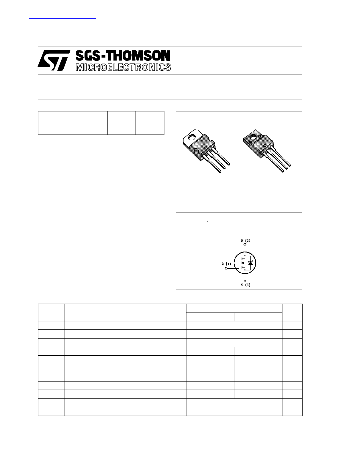
3
2
1
1
TO-220 ISOWATT220
INTERNAL SCHEMATIC DIAGRAM
3
2
ABSOLUTE MAXIMUM RATINGS
Symb o l Paramet er Val u e Unit
STP 15N06L ST P15N06LF I
V
V
V
I
DM
P
V
T
(•) Pulsewidth limited bysafe operating area
July 1993
Drain - s ource Voltage (VGS=0) 60 V
DS
Drain- gate Voltage (RGS=20kΩ)60V
DGR
Gate-source Voltage ± 15 V
GS
Drain Current (continuous) at Tc=25oC1510A
I
D
Drain Current (continuous) at Tc=100oC10 7A
I
D
(•) Drain Current (pulsed) 60 60 A
Total D i ssipation at Tc=25oC7035W
tot
Derat ing Factor 0.47 0.23 W/
Ins ulation Withs t and Voltage (DC) 2000 V
ISO
St or a ge Tem perature -65 to 175
stg
Max. Operating Junctio n Temperatur e 175
T
j
o
o
o
C
C
C
1/10
STP15N06L/FI
THERMAL DATA
TO-220 ISOW ATT 220
R
thj-case
R
thj-amb
R
thc-sink
T
AVALANCHE CHARACTERISTICS
Symbol Parameter Max Value Uni t
I
AR
E
E
I
AR
Thermal Resistance Junction - cas e M ax 2.14 4.29
Thermal Resistance Junction- ambient Max
Thermal Resistance Case-sink Typ
Maximum Lead T emperature For Soldering Purp ose
l
Avalanc h e Cu rr ent , Repet itive or Not-R epetitive
(pulse width limited by Tjmax, δ <1%)
Single Pul se Avalanche Ener gy
AS
(starti ng T
Repetitive Avalanc he Energ y
AR
=25oC, ID=IAR,VDD=25V)
j
(pulse width limited by Tjmax, δ <1%)
Avalanc h e Cu rr ent , Repet itive or Not-R epetitive
(Tc= 100oC, puls e width limited by Tjmax, δ <1%)
62.5
0.5
300
15 A
40 mJ
10 mJ
10 A
o
C/W
o
C/W
o
C/W
o
C
ELECTRICAL CHARACTERISTICS (T
=25oC unless otherwise specified)
case
OFF
Symbol Parameter Test Co ndition s Min. Typ. Max. Unit
V
(BR)DSS
Drain - s ource
ID=250µAVGS=0 60 V
Break d own Volta ge
I
DSS
I
GSS
Zer o Gate Voltage
Drain Current (VGS=0)
Gat e- body Leakage
Current (V
DS
=0)
VDS=MaxRating
VDS= Max R ating x 0.8 Tc=125oC
= ± 15 V ± 100 nA
V
GS
250
1000µAµA
ON (∗)
Symbol Parameter Test Co ndition s Min. Typ. Max. Unit
V
GS(th)
R
DS(on)
I
D(on)
Gate Threshold Voltage VDS=VGSID=250µA11.62.5V
St at ic Drain-s our ce O n
Resistance
On St ate Dra in Current VDS>I
VGS=5 V ID=7.5A
VGS=5 V ID=7.5A Tc=100oC
D(on)xRDS(on)max
0.115 0.15
0.3
15 A
VGS=10 V
DYNAMIC
Symbol Parameter Test Co ndition s Min. Typ. Max. Unit
(∗)Forward
g
fs
Tr ansconductance
C
C
C
Input Capacitance
iss
Out put Capacitance
oss
Reverse Transfer
rss
Capacitance
VDS>I
D(on)xRDS(on)maxID
=7.5A 5 9 S
VDS=25V f=1MHz VGS=0 350
150
50
500
200
80
Ω
Ω
pF
pF
pF
2/10
STP15N06L/FI
ELECTRICAL CHARACTERISTICS (continued)
SWITCHING ON
Symbol Parameter Test Co ndition s Min. Typ. Max. Unit
t
d(on)
(di/dt)
Q
Q
Q
Turn-on Time
t
Rise Time
r
Turn-on C urrent Slope VDD=40V ID=15A
on
Total Gate Charge
g
Gat e- Source Charge
gs
Gate-Drain Charge
gd
SWITCHING OFF
Symbol Parameter Test Co ndition s Mi n. Ty p. Max. Unit
t
r(Voff)
t
Off -voltage R ise Time
t
Fall Time
f
Cross-over Time
c
SOURCE DRAIN DIODE
VDD=25V ID=7.5A
RG=50 Ω VGS=5V
60
19090270
(see test circuit, figure 3)
120 A/µs
RG=50 Ω VGS=5V
(see test circuit, figure 5)
VDD=40V ID=15A VGS=5V 12
7
4
VDD=40V ID=15A
RG=50 Ω VGS=5V
(see test circuit, figure 5)
40
60
110
18 nC
60
90
160
ns
ns
nC
nC
ns
ns
ns
Symbol Parameter Test Co ndition s Mi n. Ty p. Max. Unit
I
I
SDM
SD
Source-drain Current
(•)
Source-drain Current
15
60
(pulsed)
V
(∗) For w ar d On Volt age ISD=15A VGS=0 1.5 V
SD
t
Reverse Recovery
rr
Time
Q
Reverse Recovery
rr
ISD= 15 A di/ dt = 100 A/µs
VDD=25V Tj=150oC
(see test circuit, figure 5)
80
0.18
Charge
I
RRM
Reverse Recovery
4.5
Current
(∗) Pulsed:Pulse duration = 300 µs, dutycycle 1.5 %
(•) Pulse widthlimited by safeoperating area
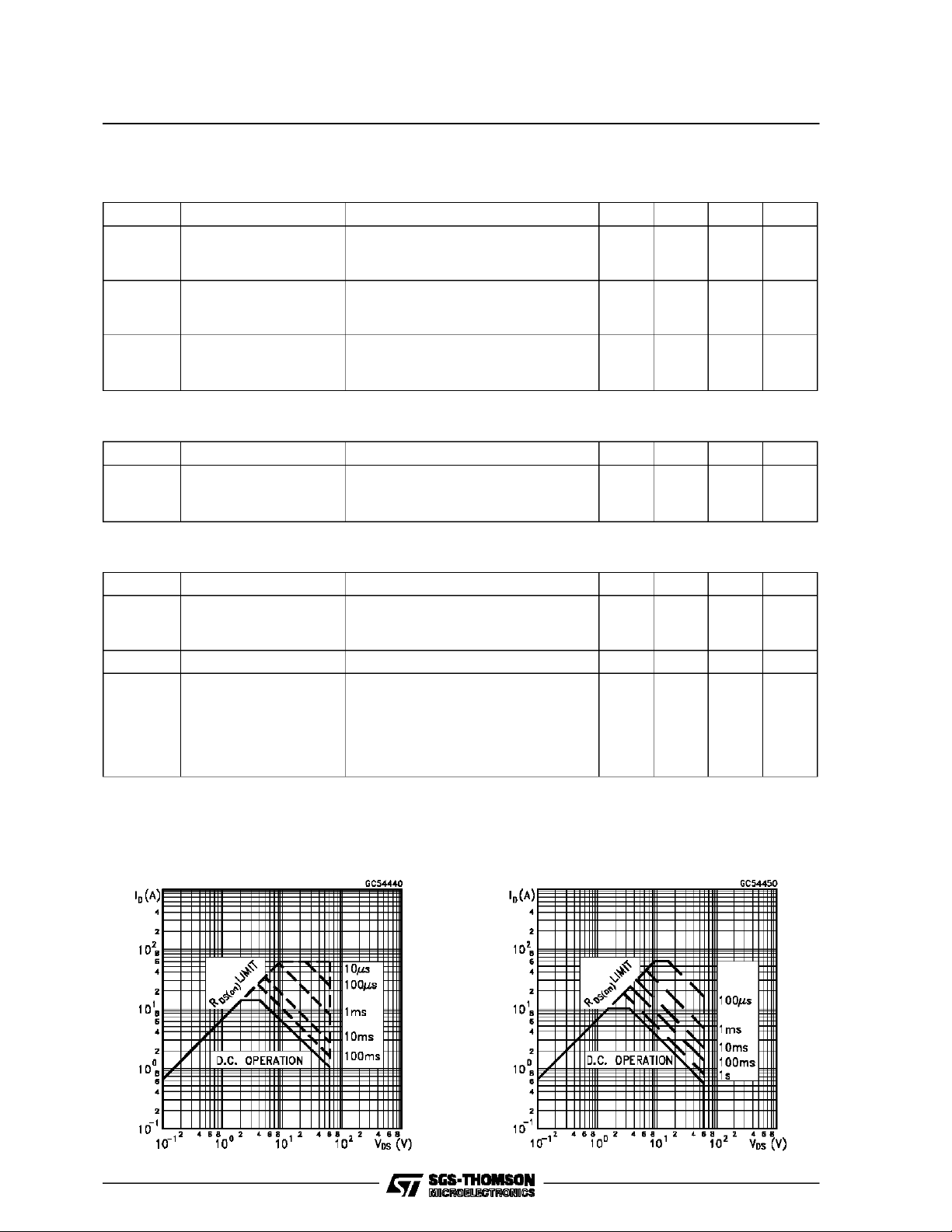
Safe Operating Areas For TO-220 Safe Operating Areas For ISOWATT220
A
A
ns
µC
A
3/10

STP15N06L/FI
Thermal Impedance For TO-220
Derating Curve For TO-220
Thermal Impedance For ISOWATT220
Derating Curve For ISOWATT220
Output Characteristics
4/10
Transfer Characteristics

Transconductance Static Drain-source On Resistance
Gate Charge vs Gate-source Voltage Capacitance Variations
STP15N06L/FI
Temperature
Normalized On Resistance vs TemperatureNormalized Gate Threshold Voltage vs
5/10

STP15N06L/FI
Turn-on Current Slope Turn-off Drain-source Voltage Slope
Cross-over Time Switching Safe Operating Area
Accidental Overload Area Source-drain Diode Forward Characteristics
6/10

STP15N06L/FI
Fig. 1: Unclamped Inductive Load Test Circuits
Fig. 3: Switching Times Test Circuits For
Resistive Load
Fig. 2: Unclamped Inductive Waveforms
Fig. 4: Gate Charge Test Circuit
Fig. 5: Test Circuit For Inductive Load Switching
And Diode Reverse Recovery Time
7/10

STP15N06L/FI
TO-220 MECHANICAL DATA
DIM.
mm inch
MIN. TYP. MAX. MIN. TYP. MAX.
A 4.40 4.60 0.173 0.181
C 1.23 1.32 0.048 0.051
D 2.40 2.72 0.094 0.107
D1 1.27 0.050
E 0.49 0.70 0.019 0.027
F 0.61 0.88 0.024 0.034
F1 1.14 1.70 0.044 0.067
F2 1.14 1.70 0.044 0.067
G 4.95 5.15 0.194 0.203
G1 2.4 2.7 0.094 0.106
H2 10.0 10.40 0.393 0.409
L2 16.4 0.645
L4 13.0 14.0 0.511 0.551
L5 2.65 2.95 0.104 0.116
L6 15.25 15.75 0.600 0.620
L7 6.2 6.6 0.244 0.260
L9 3.5 3.93 0.137 0.154
DIA. 3.75 3.85 0.147 0.151
E
A
L4
D
F2
F1
G1
H2
G
F
C
D1
L2
Dia.
L5
L7
L6
L9
P011C
8/10

ISOWATT220 MECHANICAL DATA
STP15N06L/FI
DIM.
MIN. TYP. MAX. MIN. TYP. MAX.
A 4.4 4.6 0.173 0.181
B 2.5 2.7 0.098 0.106
D 2.5 2.75 0.098 0.108
E 0.4 0.7 0.015 0.027
F 0.75 1 0.030 0.039
F1 1.15 1.7 0.045 0.067
F2 1.15 1.7 0.045 0.067
G 4.95 5.2 0.195 0.204
G1 2.4 2.7 0.094 0.106
H 10 10.4 0.393 0.409
L2 16 0.630
L3 28.6 30.6 1.126 1.204
L4 9.8 10.6 0.385 0.417
L6 15.9 16.4 0.626 0.645
L7 9 9.3 0.354 0.366
Ø 3 3.2 0.118 0.126
mm inch
E
A
D
B
L3
L6
L7
Ø
F1
H
L2
F2
F
123
L4
G1
G
P011G
9/10

STP15N06L/FI
Information furnished isbelieved to be accurateand reliable. However, SGS-THOMSONMicroelectronics assumes noresponsability for the
consequences of use of suchinformation nor for any infringementof patents orother rights of third parties whichmay results from its use. No
license isgrantedby implicationor otherwiseunder anypatentor patentrights ofSGS-THOMSON Microelectronics.Specificationsmentioned
in this publicationare subjectto change without notice.This publication supersedes and replacesall information previouslysupplied.
SGS-THOMSON Microelectronicsproducts arenotauthorizedfor useascriticalcomponents inlifesupportdevices orsystemswithout express
written approvalof SGS-THOMSON Microelectonics.
1994 SGS-THOMSONMicroelectronics - All Rights Reserved
Australia - Brazil- France - Germany -Hong Kong -Italy - Japan - Korea - Malaysia -Malta - Morocco - The Netherlands -
Singapore -Spain - Sweden- Switzerland -Taiwan - Thailand - United Kingdom -U.S.A
SGS-THOMSON Microelectronics GROUP OF COMPANIES
10/10
 Loading...