

1
3
3
查询STB140NF55供应商
N-CHANNEL 55V - 0.0065 Ω - 80A TO-220/D²PAK
TYPE
STB140NF55
STP140NF55
■ TYPICAL R
V
DSS
55 V
55 V
(on) = 0.0065 Ω
DS
DESCRIPTION
This Power Mosfet is the latest development of
STMicroelectronis unique "Single Feature Size™"
strip-based process. The resulting transistor
shows extremely high p acking density for low onresistance, rugged ava lanche characteristics and
less critical alignment steps therefore a remarkable manufacturing reproducibility.
R
DS(on)
< 0.008 Ω
< 0.008 Ω
I
D
80 A
80 A
STB140NF55
STP140NF55
STripFET™ II POWER MOSFET
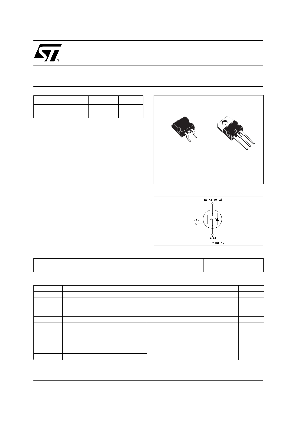
Figure 1:PackageTable 1: General Features
1
D2PAK
TO-263
(Suffix “T4”)
TO-220
2
APPLICATIONS
■ MOTOR CONTROL
■ HIGH CURRENT, SWITCHING
Figure 2: Internal Schematic Diagram
APPLICATIONS
■ AUTOMOTIVE ENVIRONMENT
Table 2: Order Codes
STB140NF55T4
STP140NF55
Part Number MARKING PACKAGE PACKAGING
B140NF55
P140NF55
D²PAK
TO-220
TAPE & REEL
TUBE
Table 3:ABSOLUTE MAXIMUM RATINGS
Symbol Parameter Value Unit
V
DS
V
GS
I
D
I
D
I
(•)
DM
P
tot
dv/dt
E
AS
T
stg
T
j
(•) Pulse width limited by safe operating area.
(**) Current Limited by Package
Drain-source Voltage (VGS = 0)
55 V
Gate- source Voltage ± 20 V
Drain Current (conti nuo us ) at TC = 25°C
Drain Current (conti nuo us ) at TC = 100°C
80 A
80 A
Drain Current (pulse d) 320 A
Total Dissipation at TC = 25°C
300 W
Derating Factor 2 W/°C
(1)
Peak Diode Recove ry vo ltag e slo pe 10 V/ns
(2)
Single Pulse Avalanche Energy 1.3 mJ
Storage Temperature
Operating Junction Temperature
(1) ISD ≤80A, di/dt ≤300A/µs, VDD ≤ V
(2) Starting Tj = 25 oC, ID = 40A, VDD = 30V
-55 to 175 °C
(BR)DSS
, Tj ≤ T
JMAX
Rev. 2
1/11December 2004
STB140NF55 STP140NF55
Table 4: THERMAL DATA
Rthj-case
Rthj-amb
T
Thermal Resistance Junction-case
Thermal Resistance Junction-ambient
Maximum Lead Temperature For Soldering Purpose
l
Max
Max
0.5
62.5
300
°C/W
°C/W
°C
ELECTRICAL CHARACTERISTICS (T
= 25 °C unless otherwise specified)
case
Table 5: OFF
Symbol Parameter Test Conditions Min. Typ. Max. Unit
V
(BR)DSS
Drain-source
I
= 250 µA, VGS = 0
D
55 V
Breakdown Voltage
= Max Rating
I
DSS
I
GSS
Table 6: ON
Zero Gate Voltage
Drain Current (V
Gate-body Leakage
Current (V
(*)
DS
= 0)
GS
= 0)
V
DS
= Max Rating TC = 125°C
V
DS
= ± 20 V
V
GS
1
10
±100 nA
Symbol Parameter Test Conditions Min. Typ. Max. Unit
V
GS(th)
R
DS(on)
Gate Threshold Voltage
Static Drain-source On
V
= VGS ID = 250 µA
DS
V
= 10 V ID = 40 A
GS
234V
0.0065 0.008 Ω
Resistance
Table 7: DYNAMIC
Symbol Parameter Test Conditions Min. Typ. Max. Unit
(*)
g
fs
C
iss
C
oss
C
rss
Forward Transconductance
Input Capacitance
Output Capacitance
Reverse Transfer
Capacitance
V
25 V ID=40 A
DS =
V
= 25V f = 1 MHz VGS = 0
DS
100 S
5300
1000
290
µA
µA
pF
pF
pF
2/11
STB140NF55 STP140NF55
ELECTRICAL CHARACTERISTICS (continued)
Table 8: SWITCHING ON
Symbol Parameter Test Conditions Min. Typ. Max. Unit
t
d(on)
Q
Q
Q
t
r
g
gs
gd
Turn-on Delay Time
Rise Time
Total Gate Charge
Gate-Source Charg e
Gate-Drain Charge
Table 9: SWITCHING OFF
Symbol Parameter Test Conditions Min. Typ. Max. Unit
t
d(off)
t
f
Turn-off Delay Time
Fall Time
Table 10: SOURCE DRAIN DIODE
Symbol Parameter Test Conditions Min. Typ. Max. Unit
I
SD
I
SDM
V
SD
t
rr
Q
rr
I
RRM
(*)
Pulsed: Pulse duration = 300 µs, duty cycle 1.5 %.
(
•)Pulse width limited by safe operating area.
Source-drain Curre nt
)
Source-drain Curre nt (pu lse d)
(•
(*)
Forward On Voltage
Reverse Recovery Time
Reverse Recovery Charge
Reverse Recovery Current
= 27.5 V ID = 40 A
V
DD
=4.7 Ω VGS = 10 V
R
G
(Resistive Load, Figu re 3)
V
= 44V ID= 80A VGS= 10V
DD
V
= 27.5 V ID = 40 A
DD
=4.7 Ω VGS = 10 V
R
G
(Resistive Load, Figu re 3)
I
= 80 A VGS = 0
SD
I
= 80 A di/dt = 100A/µs
SD
= 20 V Tj = 150°C
V
DD
(see test circuit, Figure 5)
30
150
142
27
55
125
45
80
320
1.5 V
90
275
6.5
ns
ns
nC
nC
nC
ns
ns
A
A
ns
µC
A
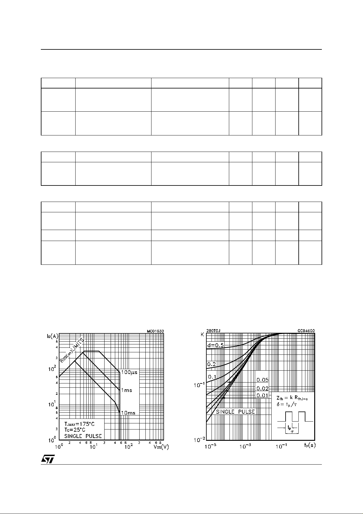
Figure 3: Safe Operating Area
Figure 4: Therm al Im pe da nce
3/11
STB140NF55 STP140NF55
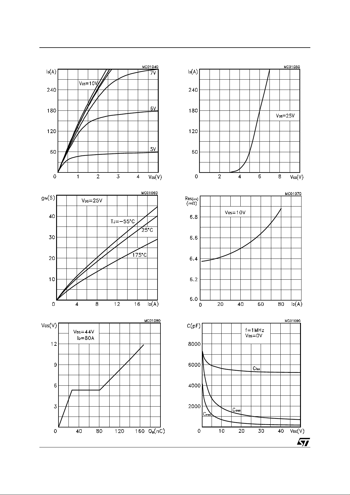
Figure 5: Output Characteristics Figure 6: Transfer Char ac ter ist ics
Figure 7: Transconductance Figure 8: Static Drain-source On Resistance
Figure 9: Gate Charge vs Gate-source Voltage Figure 10: Capacitance Variations
4/11
 Loading...