

ST STP130NS04ZB, STB130NS04ZB, STW130NS04ZB User Manual
查询STB130NS04ZB供应商
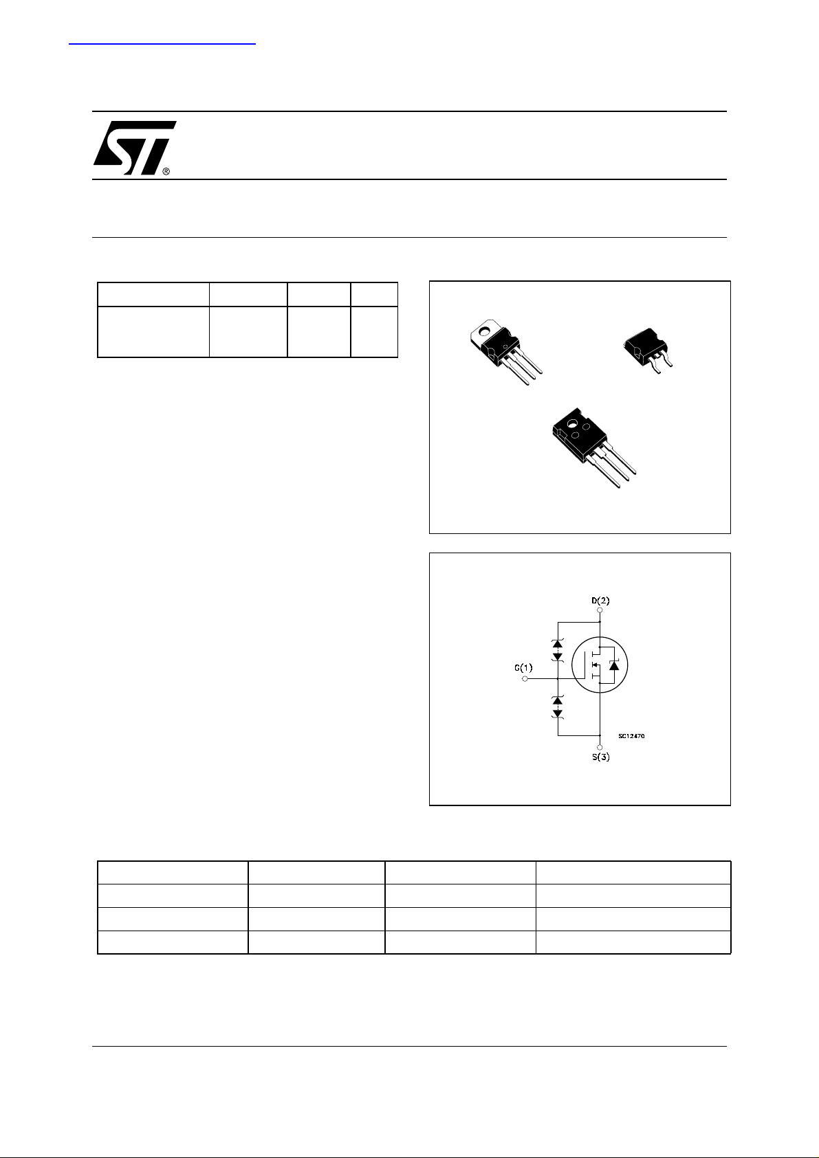
N-CHANNEL CLAMPED - 7 mΩ - 80A TO-220/D²PAK/TO-247
FULLY PROTECTED MESH OVERLAY™ MOSFET
STP130NS04ZB
STB130NS04ZB - STW130NS04ZB
Table 1: Ge neral Features
TYPE V
STP130NS04ZB
STB130NS04ZB
STW130NS04ZB
■ TYPICAL R
■ 100% AVALANCHE TESTED
■ LOW CAPACITAN CE AND GATE CHARGE
■ 175°C MAXIMUM JUNCTION TEMPERA TURE
(on) = 7 mΩ
DS
DSS
CLAMPED
CLAMPED
CLAMPED
R
DS(on)
< 9 mΩ
< 9 mΩ
< 9 mΩ
I
D
80 A
80 A
80 A
DESCRIPTION
This fully clamped MO SFE T is produced by usi ng
the latest advanced Company’s Mesh Overlay
process which is based on a novel strip layout.
The inherent benefits of the new technology coupled with the extra clamping capabilities make this
product particularly suitable for the harshest operation conditions such as those encountered in the
automotive environment .Any other application requiring extra ruggedness is also recommended.
APPLICATIONS
■ HIGH SWITCHING CURRENT
■ LINEAR APPLICATIONS
Figure 1: Package
TO-220
3
2
1
1
TO-247
D²PAK
3
2
1
Figure 2: Internal Schematic Diagram
3
Table 2: Order Codes
Sales Type Marking Package Packaging
STP130NS04ZB P130NS04ZB TO-220 TUBE
STB130NS04ZBT4 B130NS04ZB D²PAK TAPE & REEL
STW130NS04ZB W130NS04ZB TO-247 TUBE
Rev. 2
1/12February 2005
STP130NS04ZB - STB130NS04ZB - STW130NS04ZB
Table 3: Absolute Maximum ratings
Symbol Parameter Value Unit
V
DS
V
DG
V
GS
I
D
I
D
I
DG
I
GS
I
DM
P
TOT
V
ESD(G-S)
T
j
T
stg
() Pulse wi dt h l i m i ted by safe opera t in g area
Table 4: Thermal Data
Rthj-case Thermal Resistance Junction-case Max 0.50 °C/W
Rthj-pcb (*) Thermal Resistance Junction-pcb Max -- 35 -- °C/W
Rthj-a Thermal Resistance Junction-ambient Max 62.5 -- 50
T
l
(*)Whe n m ounted on 1 inch ² FR4 2oZ Cu
Drain-source Voltage (VGS = 0)
CLAMPED V
Drain-gate Voltage CLAMPED V
Gate- source Voltage CLAMPED V
Drain Current (continuous) at TC = 25°C
Drain Current (continuous) at TC = 100°C
80 A
60 A
Drain Gate Current (continuous) ± 50 mA
Gate Source Current (continuous) ± 50 mA
()
Drain Current (pulsed) 320 A
Total Dissipation at TC = 25°C
300 W
Derating Factor 2.0 W/°C
Gate-Source ESD(HBM-C=100 pF, R=1.5 KΩ) 4KV
Max Operating Junction Temperature
Storage Temperature
-55 to 175 °C
TO-220 D²PAK TO-247 Unit
Maximum Lead Temperature For Soldering
300 °C
Purpose (1.6 mm from case, for 10 sec)
Table 5: Avalanche Characteristics
Symbol Parameter Max Value Unit
I
AR
E
AS
Avalanche Current, Repetitive or Not-Repetitive
(pulse width limited by T
max)
j
Single Pulse Avalanche Energy
(starting T
= 25 °C, ID = IAR, VDD = 30 V)
j
80 A
500 mJ
2/12

STP130NS04ZB - STB130NS04ZB - S TW130NS04ZB
ELECTRICAL CHARACTERISTICS (T
=25°C UNLESS OTHERWISE SPECIFIED)
CASE
Table 6: On/Off
Symbol Parameter Test Conditions Min. Typ. Max. Unit
V
(BR)DSS
Clamped Voltage ID = 1 mA, VGS = 0
33 V
-40 < Tj < 175 °C
I
I
V
DSS
GSS
GSS
Zero Gate Voltage
Drain Current (V
GS
Gate-body Leaka ge
Current (V
DS
= 0)
Gate-Source
= 0)
V
= 16 V,Tj = 25 °C
DS
V
= 16 V,Tj = 125 °C
DS
V
= ±10 V,Tj = 25 °C10µA
GS
10
100
IGS = ±100 µA 18 V
Breakdown Voltage
V
V
GS(th)
R
DS(on)
Gate Threshold Voltage
Static Drain-source On
= VGS = ID = 1 mA 2 4 V
DS
VGS = 10 V ,ID = 40 A 7 9
Resistance
Table 7: Dynamic
Symbol Parameter Test Conditions Min. Typ. Max. Unit
Forward Transconductance VDS = 15 V, ID = 40 A 50 S
g
fs
C
C
C
t
d(on)
t
d(off)
Q
Q
Q
iss
oss
rss
t
f
t
f
gs
gd
g
Input Capacitance
Output Capacitance
Reverse Transfer
Capacitance
Turn-on Delay Time
Fall Time
Turn-off Delay Time
Fall Time
Total Gate Charge
Gate-Source Charge
Gate-Drain Charge
= 25 V, f = 1MHz, VGS = 0 2700
V
DS
= 17.5 V, ID = 40 A,
V
DD
RG = 4.7 Ω, V
GS
= 10 V
(see Figure 15)
VDD = 20 V, ID = 80 A,
VGS = 10 V
(see Figure 17)
1275
285
40
220
170
100
80
20
27
105 nC
m
pF
pF
pF
ns
ns
ns
ns
nC
nC
µA
µA
Ω
Table 8: Source Drain Diode
Symbol Parameter Test Conditions Min. Typ. Max. Unit
I
SD
I
(2)
SDM
(1)
V
SD
t
rr
Q
rr
I
RRM
(1) Pulsed: Pulse durat i on = 300 µs, duty cycle 1.5 %.
(2) Pulse width limite d by safe operating area.
Source-drain Current
Source-drain Current (pulsed)
Forward On Voltage
Reverse Recovery Time
Reverse Recovery Charge
Reverse Recovery Current
ISD = 80 A, VGS = 0
= 80 A, di/dt = 100A/µs
I
SD
V
= 25V, Tj = 150°C
DD
(see Figure 16)
90
0.18
4
80
320
1.5 V
A
A
ns
µC
A
3/12
STP130NS04ZB - STB130NS04ZB - STW130NS04ZB
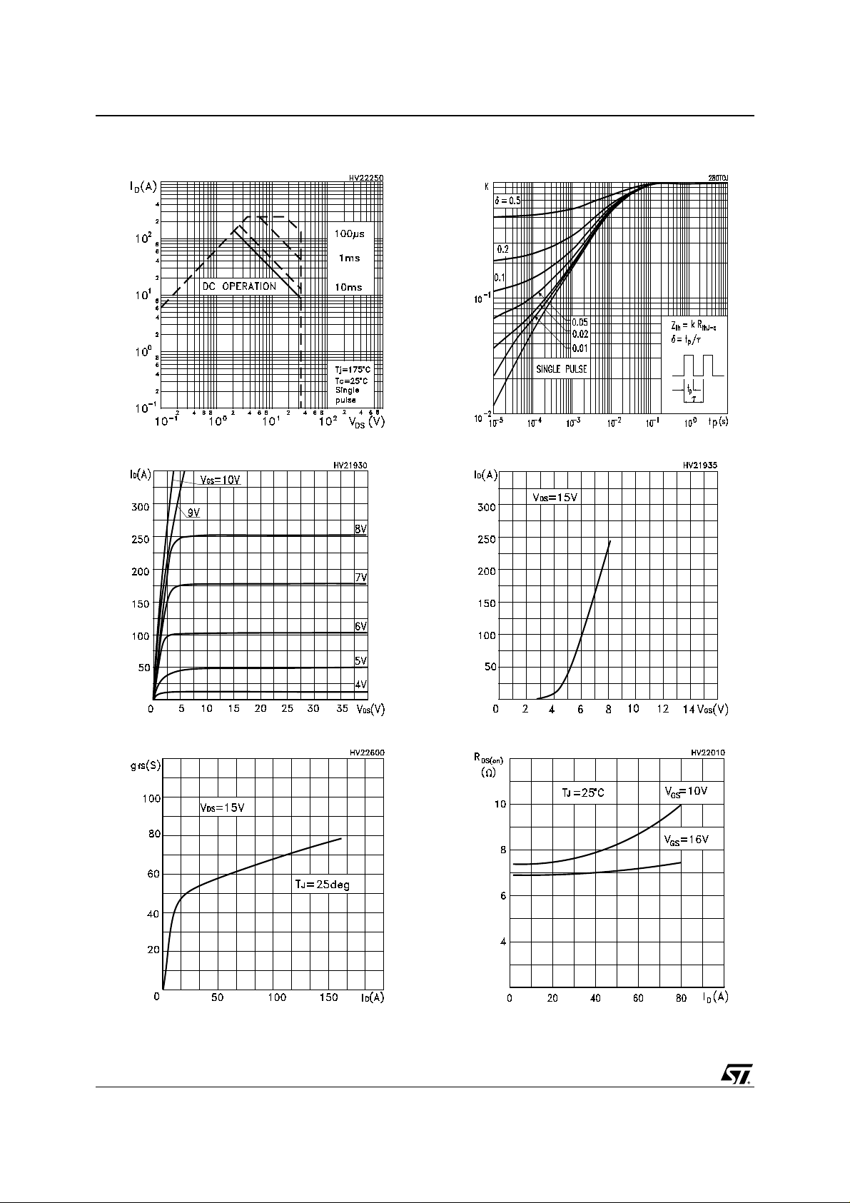
Figure 3: Safe Operating Area
Figure 4: Output Characteristics
Figure 6: Thermal Impedance
Figure 7: Transfer Characteristics
Figure 5: Transconductance
4/12
Figure 8: Static Drain-source On Resistance
 Loading...