

1
3
3
查询STMAV340供应商
STripFET™ III Power MOSFET for DC-DC Conversion
General features
STB120NH03L
STP120NH03L
N-Channel 30V - 0.005Ω - 9A - TO-220/D2PAK
Type
STB120NH03L
STP120NH03L
■ Typical R
■ R
■ Conduction Losses Reduced
■ Switching Losses Reduced
■ Low Threshold Device
*Qg Industry’s Benchmark Low
DS(on)
V
DSS
30V
30V
= 0.005Ω @ 10V
DS(on)
R
DS(on)
<0.0055Ω
<0.0055Ω
I
D
9A Note 1
9A Note 1
Description
These devices utilizes the latest advanced design
rules of ST’s proprietary STripFET™ technology.
It is ideal in high performanc e DC-DC converter
applications where efficiency is to be achieved at
very high output currents.
Applications
■ Specifically designed and optimized for high
efficiency DC-DC converters
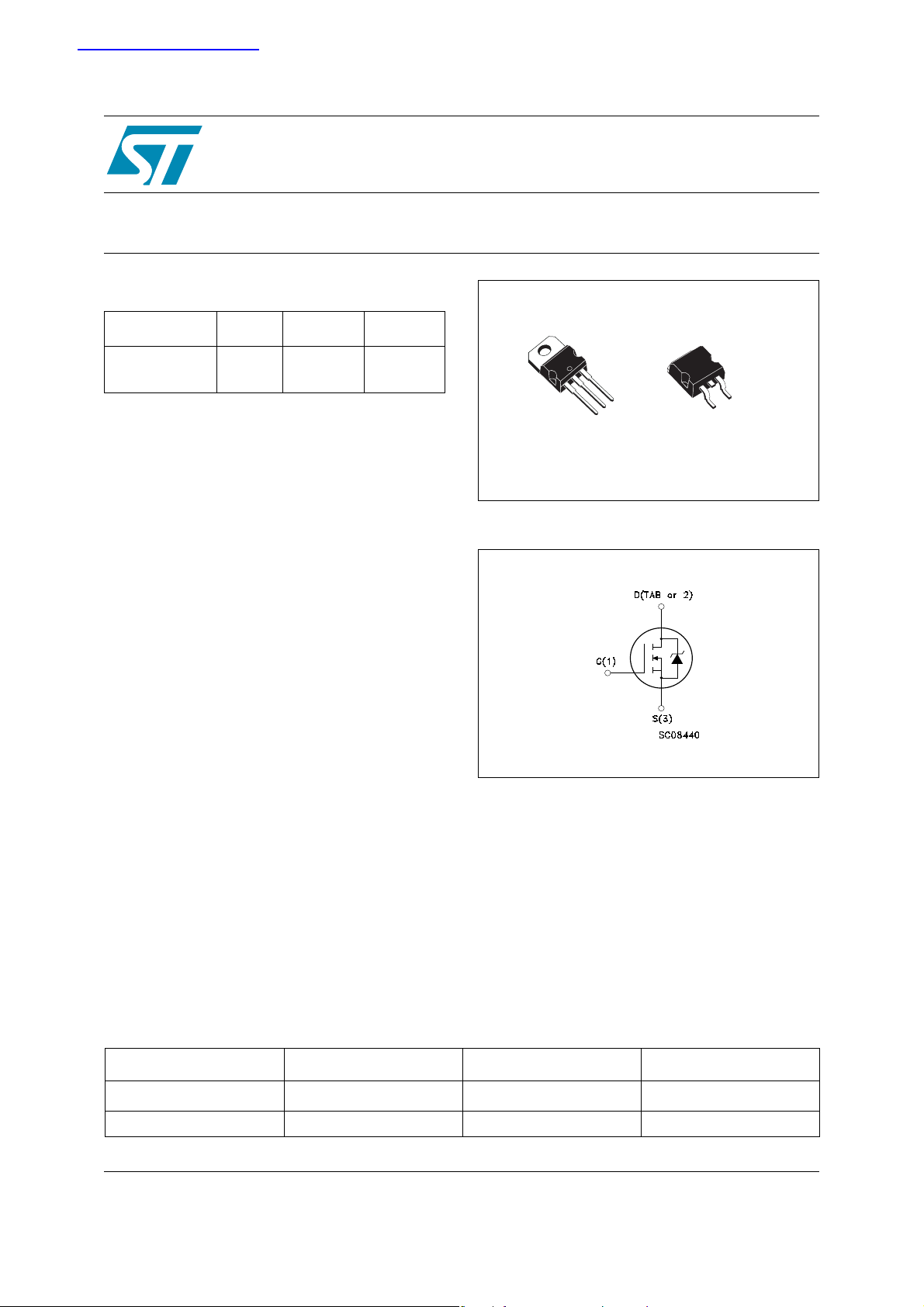
2
TO-220
1
D2PAK
Internal schematic diagram
Order codes
Part Number Marking Package Packaging
STB120NH03L B120NH03L
STP120NH03L P120NH03L TO-220 TUBE
December 2005 1/14
2
D
PAK
TAPE & REEL
Rev 1
www.st.com
14
1 Electrical ratings STB120NH03L - STP120NH03L
1 Electrical ratings
Table 1. Absolute maximum ratings
Symbol Parameter Value Unit
V
DS
V
DGR
V
GS
ID Note 1 Drain Current (continuous) at TC = 25°C
I
Note 1 Drain Current (continuous) at TC = 100°C
D
Note 2
I
DM
P
TOT
Drain-source Voltage (V
Drain-gate Voltage (R
GS
GS
= 0V)
= 20kΩ)
30 V
30 V
Gate-Source Voltage ± 20 V
60 A
60 A
Drain Current (pulsed ) 240 A
Total Dissip ation at TC = 25°C
115 W
Derating Factor 0.77 W/°C
EAS Note 3 Single Pulse Avalanche Energy 700 mJ
T
J
T
stg
Operating Junction Temperature
Storage Temperature
-55 to 175 °C
Table 2. Thermal data
R
R
thJC
thJA
T
Thermal Resist ance Junction-case Max 1.30 °C/W
Thermal Resist ance Junction-amb Max 62.5 °C/W
Maximum Lead Temperature For Soldering
l
Purpose
300 °C
2/14
STB120NH03L - STP120NH03L 2 Electrical characteristics
2 Electrical characteristics
( T
= 25 °C unless otherwise specified )
CASE
Table 3. On/off states
Symbol Parameter Test Conditions Min. Typ. Max. Unit
V
(BR)DSS
I
DSS
I
GSS
V
GS(th)
R
DS(on)
Drain-Source Breakdown
Voltage
Zero Gate Voltage Drain
Current (V
GS
= 0)
Gate Body Leakage Current
= 0)
(V
DS
Gate Threshold Voltage
St ati c Drai n-Source On
Resistance
I
= 250μA VGS= 0
D
= Max Ra ting,
V
DS
= Max Ra ting,TC=125°C
V
DS
= ±20V
V
GS
= VGS ID = 250µA
V
DS
V
= 10V ID = 30A
GS
V
= 5V ID = 30A
GS
30 V
1
10
±100 µA
11.82.5V
0.005
0.006
0.0055
0.0105
Table 4. Dynamic
Symbol Parameter Test Conditions Min. Typ. Max. Unit
g
fs
C
C
C
Note 4
iss
oss
rss
Forward Transconductance
Input Capacitance
Outp u t C a pacitanc e
Rev er se Transf er Capac it a n ce
Rg Gate Input Resistance
V
= 10V ID = 30A
DS
= 15V, f = 1MHz, V
V
DS
GS
f = 1MHz Gate DC Bias=0
Test Signal Level=20mV
Open Drain
= 0
40 S
4100
680
70
1.3 Ω
µA
µA
Ω
Ω
pF
pF
pF
Qoss
Qgls
Q
g
Q
gs
Q
gd
Note 5
Note 6
Total Gate Charge
Gate-Source Charge
Gate-Drain Charge
Output Charge
Third-quadrant Gate Charge
=15V, ID = 60A
V
DD
=10V
V
GS
Figure 14 on page 7
V
= 16V V
DS
V
< 0 VGS= 10V
DS
GS
= 0
57
77
11.8
7.3
27 ns
55 ns
nC
nC
nC
3/14

2 Electric al characteristics STB120NH03L - STP120NH03L
Table 5. Switching times
Symbol Parameter Test Conditions Min. Typ. Max. Unit
= 15V, ID = 30A,
V
t
d(on)
t
t
d(off)
Tur n- on D elay Ti me
r
Rise Time
Off volt age Rise Time
t
f
FallTime
DD
= 4.7Ω, V
R
G
GS
= 10V
Figure 13 on page 7
= 15V, ID = 30A,
V
DD
= 4.7Ω, V
R
G
GS
= 10V
Figure 15 on page 7
16
95
48
23
ns
ns
ns
ns
Table 6. Sour ce dr ai n di ode
Symbol Parameter Test Conditions Min. Typ. Max. Unit
V
SD
I
SD
I
SDM
Note 4
t
rr
Q
rr
I
RRM
Source-drain Current
Source-drain Current (pulsed)
Forward on Voltage
Reverse Recovery Time
Reverse Recovery Charge
Reverse Recovery Current
I
I
V
Figure 15 on page 7
Note: 1 Value limited by wire bonding
2 Pulse width limited by safe operating area
3 Starting T
= 25°C , ID = 30A, VDD = 15V
J
4 Pulsed: pulse duration = 300µs, duty cycle 1.5%
5Q
oss
= C
*Δ VIN, C
oss
= Cgd + Cds. See Power losses calculation
oss
6 Gate charge for synchronous operation.
= 30A V
SD
= 60A, di/dt = 100A/µs,
SD
= 30V, TJ =150°C
DD
GS
= 0
46
64
2.8
60
240
1.4 V
A
A
ns
nC
A
4/14
STB120NH03L - STP120NH03L 2 Electrical characteristics
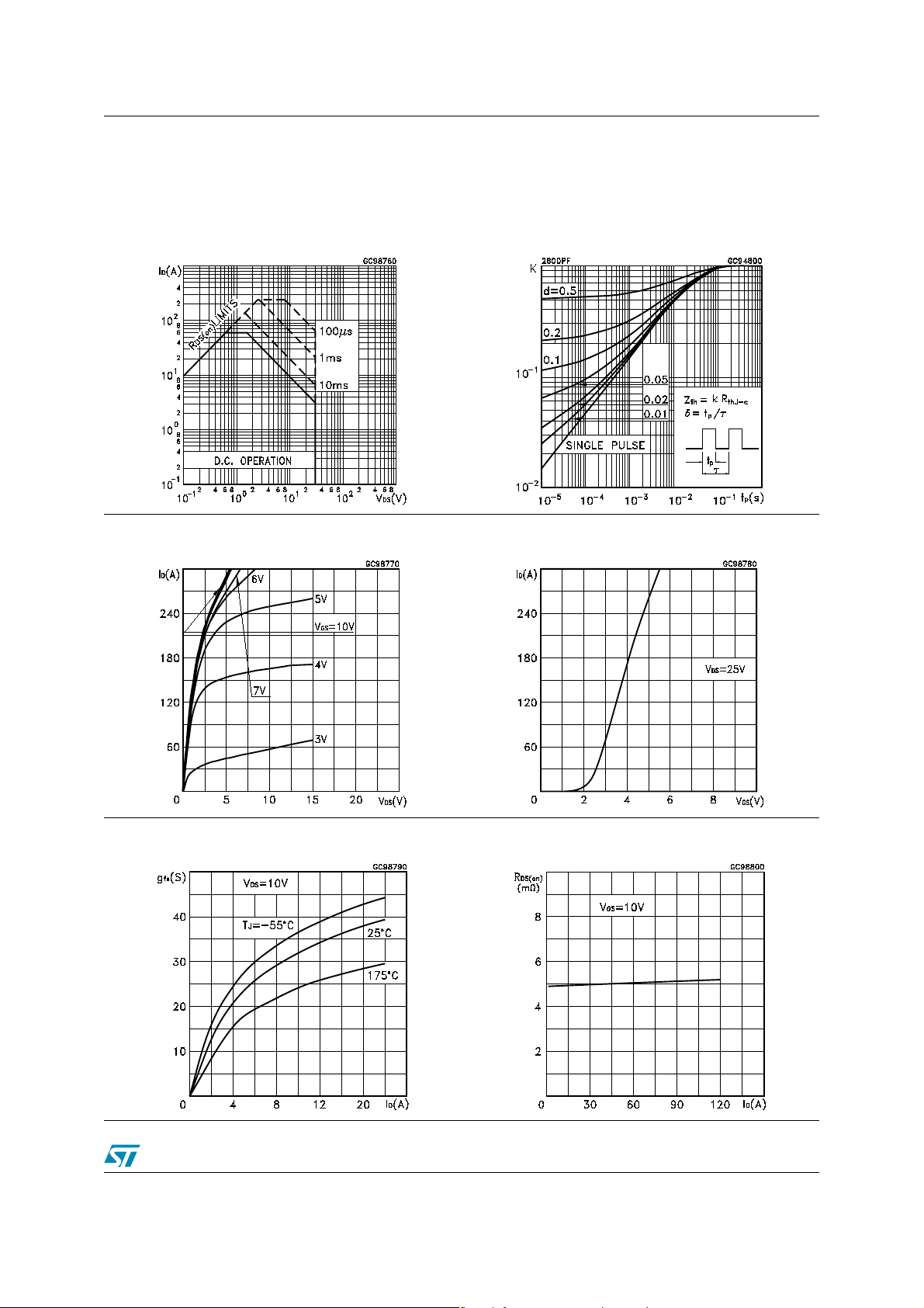
2.1 Electrical chraracteristics (curves)
Figure 1. Safe Operating Area Figure 2. Thermal Impedance
Figure 3. Output Characteristics Figure 4. Transfer Characteristics
Figure 5. Transconductance Figure 6. Static Drain-Source on Resistance
5/14
 Loading...