

ST STP11NM60, STP11NM60FP, STB11NM60, STB11NM60-1 User Manual
查询STB11NM60供应商
STP11NM60 - STP11NM60FP
STB11NM60 - STB11NM60-1
N-CHANNEL600V - 0.4Ω-11ATO-220/TO-220FP/D2PAK/I2PAK
MDmesh™Power MOSFET
TYPE V
STP11NM60
STP11NM60FP
STB11NM60
STB11NM60-1
TYPICAL RDS(on) = 0.4Ω
HIGH dv/dt AND AVALANCHE CA PABILITIES
100% AVALANCHE TESTED
LOW INPUT CAPACITANCE AND GATE
DSS
600 V
600 V
600 V
600 V
R
DS(on)
< 0.45 Ω
< 0.45 Ω
< 0.45 Ω
< 0.45 Ω
I
D
11 A
11 A
11 A
11 A
CHARGE
LOW GATE INPUT RESISTANCE
DESCRIPTION
The MDmesh ™ is a new revolutionary MOSFET
technology that associates the Multiple Drain process with the Company’s PowerMESH™ horizontal
layout. The resulting product has an outstandinglow
on-resistance, impressively high dv/dt and excellent
avalanche characteristics. The adoption of the
Company’s proprietary strip technique yields overall
dynamic performancethat is significantly better than
that of similar competition’s products.
APPLICATIONS
The MDmesh™ family isvery suitable for increasing
power density of high voltage converters allowing
system miniaturization and higher efficiencies.
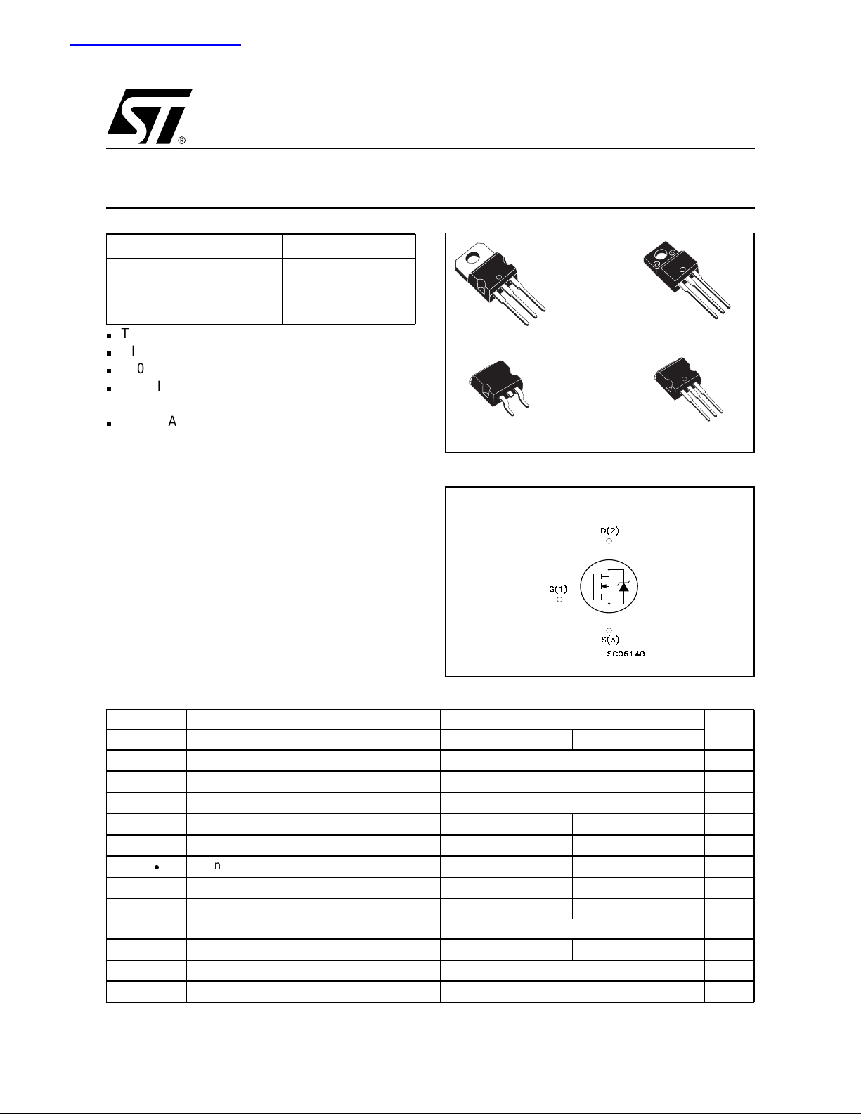
3
2
1
TO-220
1
D2PAK
3
TO-220FP
I2PAK
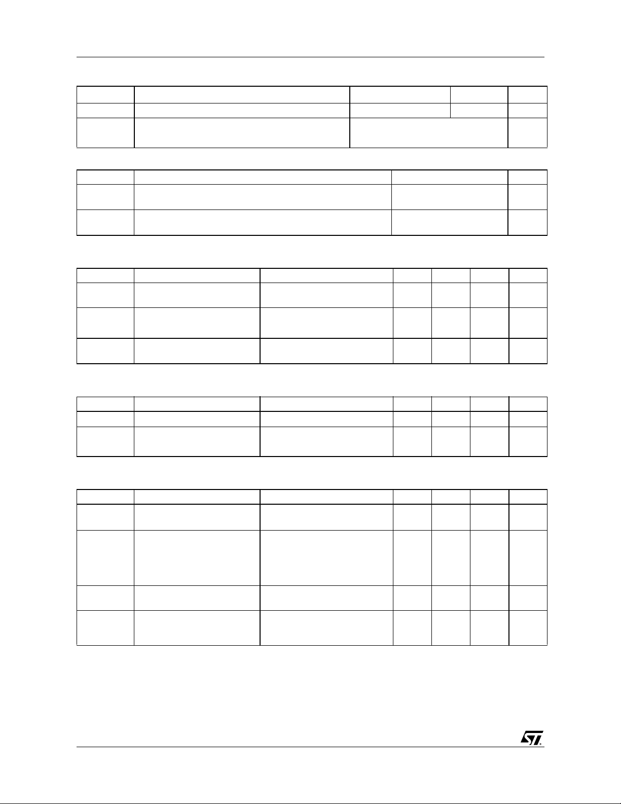
INTERNAL SCHEMATIC DIAGRAM
3
2
1
3
2
1
ABSOLUTE MAXIMUM RATINGS
Symbol Parameter Value Unit
STP(B)11NM60(-1) STP11NM60FP
V
DS
V
DGR
V
GS
I
D
I
D
I
DM
P
TOT
dv/dt(1) Peak Diode Recovery voltage slope 15 V/ns
V
ISO
T
stg
T
j
(•)Pulse width limited by safe operating area
Drain-source Voltage (VGS=0)
Drain-gate Voltage (RGS=20kΩ)
600 V
600 V
Gate- source Voltage ±30 V
Drain Current (continuous) at TC= 25°C
Drain Current (continuous) at TC= 100°C
()
Drain Current (pulsed) 44 44 (*) A
Total Dissipation at TC= 25°C
11 11 (*) A
7 7 (*) A
160 35 W
Derating Factor 1.28 0.28 W/°C
Insulation Winthstand Voltage (DC) -- 2500 V
Storage Temperature –65 to 150 °C
Max. Operating Junction Temperature 150 °C
(*)Limited only by maximum temperature allowed
<11A, di/dt<400A/µs, VDD<V
(1)I
SD
(BR)DSS,TJ<TJMAX
1/12May 2003
STP11NM60 / STP11NM60FP / STB11NM60 / STB11NM60-1
THERMAL DATA
TO-220/D2PAK/I2PAK
Rthj-case Thermal Resistance Junction-case Max 0.78 3.57 °C/W
Rthj-amb Thermal Resistance Junction-ambient Max 62.5 °C/W
T
l
Maximum Lead Temperature For Soldering Purpose 300 °C
AVALANCHE CHARACTERISTICS
Symbol Parameter Max Value Unit
I
AR
E
AS
Avalanche Current, Repetitive or Not-Repetitive
(pulse width limited by T
max)
j
Single Pulse Avalanche Energy
(starting T
= 25 °C, ID=IAR,VDD=50V)
j
TO-220FP
5.5 A
350 mJ
ELECTRICAL CHARACTERISTICS (T
= 25 °C UNLESS OTHERWISE SPECIFIED)
CASE
OFF
Symbol Parameter Test Conditions Min. Typ. Max. Unit
V
(BR)DSS
Drain-source
ID= 250 µA, VGS= 0 600 V
Breakdown Voltage
I
DSS
I
GSS
Zero Gate Voltage
Drain Current (V
GS
Gate-body Leakage
Current (V
DS
=0)
=0)
V
= Max Rating
DS
= Max Rating, TC= 125 °C
V
DS
V
= ±30V ±100 nA
GS
1µA
10 µA
ON (1)
Symbol Parameter Test Conditions Min. Typ. Max. Unit
V
GS(th)
R
DS(on)
Gate Threshold Voltage
Static Drain-source On
V
DS=VGS,ID
VGS=10V,ID= 5.5A
= 250µA
345V
0.4 0.45 Ω
Resistance
DYNAMIC
Symbol Parameter Test Conditions Min. Typ. Max. Unit
(1) Forward Transconductance VDS>I
g
fs
C
iss
C
oss
C
rss
Input Capacitance
Output Capacitance 230 pF
Reverse Transfer
Capacitance
C
(2) Equivalent Output
oss eq.
Capacitance
R
G
1. Pulsed:Pulse duration = 300 µs, duty cycle1.5%.
2. C
Gate Input Resistance f=1 MHz Gate DC Bias = 0
is defined as a constant equivalent capacitance giving the same charging time as C
oss eq.
V
.
DSS
D(on)xRDS(on)max,
ID= 5.5A
V
=25V,f=1MHz,VGS=0
DS
VGS=0V,VDS= 0V to 480V 100 pF
Test Signal Level = 20mV
Open Drain
5.2 S
1000 pF
25 pF
1.6 Ω
when VDSincreases from 0 to 80%
oss
2/12

STP11NM60 / STP11NM60FP / STB11NM60 / STB11NM60-1
ELECTRICAL CHARACTERISTICS (CONTINUED)
SWITCHING ON
Symbol Parameter Test Conditions Min. Typ. Max. Unit
V
t
d(on)
Q
Q
Q
t
r
gs
gd
Turn-on Delay Time
Rise Time 20 ns
Total Gate Charge
g
Gate-Source Charge 10 nC
Gate-Drain Charge 15 nC
SWITCHING OFF
Symbol Parameter Test Conditions Min. Typ. Max. Unit
t
r(Voff)
t
f
t
c
Off-voltage Rise Time
Fall Time 11 ns
Cross-over Time 19 ns
SOURCE DRAIN DIODE
Symbol Parameter Test Conditions Min. Typ. Max. Unit
I
SD
I
SDM
VSD(1)
t
rr
Q
rr
I
rrm
t
rr
Q
rr
I
rrm
Note: 1. Pulsed: Pulse duration = 300 µs, duty cycle 1.5 %.
2. Pulse width limited by safe operating area.
Source-drain Current 11 A
(2)
Source-drain Current (pulsed) 44 A
Forward On Voltage
Reverse Recovery Time
Reverse Recovery Charge
Reverse Recovery Current
Reverse Recovery Time
Reverse Recovery Charge
Reverse Recovery Current
Safe Operating Area for TO-2 20/D2PAK/I2PAK Safe Operating Area for TO-220FP
= 300V, ID= 5.5A
DD
= 4.7Ω VGS=10V
R
G
(see test circuit, Figure 3)
V
= 400V, ID=11A,
DD
VGS=10V
V
=400V,ID= 11A,
DD
= 4.7Ω, VGS=10V
R
G
(see test circuit, Figure 5)
ISD=11A,VGS=0
= 11A, di/dt = 100A/µs,
I
SD
VDD= 100 V, Tj= 25°C
(see test circuit, Figure 5)
I
= 11A, di/dt = 100A/µs,
SD
V
= 100 V, Tj= 150°C
DD
(see test circuit, Figure 5)
20 ns
30 nC
6ns
1.5 V
390
3.8
19.5
570
5.7
20
ns
µC
A
ns
µC
A
3/12

STP11NM60 / STP11NM60FP / STB11NM60 / STB11NM60-1
Thermal Impedance for TO-220/D2PAK/I2PA K
Thermal Impedance for TO-220FP
Transfer CharacteristicsOutput Characteristics
Transconductance
4/12
Static Drain-source On Resistance
 Loading...