

ST STP11NB40, STP11NB40FP User Manual

查询STP11NB40供应商
STP11NB40
STP11NB40FP
N - CHANNEL 400V - 0.48Ω - 10.7A - TO-220/TO-220FP
PowerMESH MOSFET
TYPE V
STP11NB4 0
STP11NB4 0FP
■ TYPICALR
■ EXTREMELYHIGH dV/dt CAPABILITY
■ 100%AVALANCHETESTED
■ VERYLOW INTRINSIC CAPACITANCES
■ GATECHARGE MINIMIZED
DS(on)
DSS
400 V
400 V
= 0.48
DESCRIPTION
Using the latest high voltage MESH OVERLAY
process, STMicroelectronics has designed an
advanced family of power MOSFETs with
outstanding performances. The new patent
pending strip layout coupled with the Company’s
proprietary edge termination structure, gives the
lowest RDS(on) per area, exceptional avalanche
and dv/dt capabilities and unrivalled gate charge
and switching characteristics.
R
DS(on)
<0.55Ω
<0.55
Ω
Ω
I
D
10.7 A
6.0 A
3
2
1
TO-220 TO-220FP
INTERNAL SCHEMATIC DIAGRAM
3
2
1
APPLICATIONS
■ HIGHCURRENT, HIGHSPEEDSWITCHING
■ SWITCHMODE POWER SUPPLIES(SMPS)
■ DC-AC CONVERTERS FOR WELDING
EQUIPMENTAND UNINTERRUPTIBLE
POWERSUPPLIESAND MOTORDRIVE
ABSOLUTE MAXIMUM RATINGS
Symbol Parameter Value Unit
ST P11 NB40 ST P1 1NB40F P
V
V
V
I
DM
P
dv/ dt(
V
T
(•) Pulse width limited by safe operating area (1)ISD≤ 10.7A, di/dt ≤ 200 A/µs, VDD≤ V
September 1998
Drain-source Voltage (VGS=0) 400 V
DS
Dra in- gat e Voltage (RGS=20kΩ)
DGR
Gate -sourc e Voltage
GS
Drain Current (continuous) at Tc=25oC 10.7 6.0 A
I
D
Drain Current (continuous) at Tc=100oC6.73.8A
I
D
400 V
30 V
±
(•) Dra in C urr en t (pu lsed) 42.8 42.8 A
Total Dissipation at Tc=25oC 125 40 W
tot
Derating Factor 1.0 0.32 W/
) Peak Dio de Recove ry voltage slope 4.5 4.5 V/ns
1
Insulat ion Withst and Voltage (DC) 2000 V
ISO
St orage Temperat ur e -65 to 1 50
stg
T
Max. Op er a t ing J unctio n Tem pe r at u r e 150
j
,Tj≤T
(BR)DSS
JMAX
o
C
o
C
o
C
1/9
STP11NB40/FP
THERMAL DATA
TO-220 TO-220FP
R
thj-case
R
thj-amb
R
thc-sink
T
AVALANCHE CHARACTERISTICS
Symbol Para meter Max Val ue Uni t
I
AR
E
Ther mal Resis t an ce Junc ti on-cas e Max 1. 0 3.1 2
Ther mal Resis t an ce Junc ti on-ambien t M a x
Thermal Resistance Case-sink Typ
Maximum Lead Temper at u r e Fo r Solder ing P ur p ose
l
Avalanche Cu rr ent, Repet it iv e or Not-Repetit iv e
(pulse width limite d by T
Single Pulse Ava lanche Energy
AS
(starting T
=25oC, ID=IAR,VDD=50V)
j
max)
j
62.5
0.5
300
10.7 A
530 mJ
o
C/W
o
C/W
o
C/W
o
C
ELECTRICAL CHARACTERISTICS
=25oC unless otherwisespecified)
(T
case
OFF
Symbol Parameter Test Conditions Min. Typ. M ax. Unit
V
(BR)DSS
Drain-sourc e
=250µAVGS=0
I
D
400 V
Break d own Voltage
I
DSS
I
GSS
Zero Gate Voltage
Drain C u rr ent (V
GS
Gat e- b ody Le ak a ge
Current (V
DS
=0)
=0)
V
=MaxRating
DS
= Max Rating Tc=125oC
V
DS
=± 30 V
V
GS
1
50
± 100 nA
ON(∗)
Symbol Parameter Test Conditions Min. Typ. M ax. Unit
V
GS(th)
Gate Threshold
V
DS=VGSID
= 250µA
345V
Voltage
R
DS(on)
Static Drain-source O n
VGS=10V ID= 5 .3 A 0.48 0.55 Ω
Resistanc e
I
D(on)
On State Drain Cu rr ent VDS>I
D(on)xRDS(on)max
10.7 A
VGS=10V
DYNAMIC
Symbol Parameter Test Conditions Min. Typ. M ax. Unit
g
(∗)Forward
fs
Tr ansconduc tance
C
C
C
Input Capacit ance
iss
Out put Capacita nc e
oss
Reverse Tran sfer
rss
Capacitance
VDS>I
D(on)xRDS(on)maxID
=5.3A 5 6.5 S
VDS=25V f=1MHz VGS= 0 1250
210
22
1625
284
30
µ
µA
pF
pF
pF
A
2/9
STP11NB40/FP
ELECTRICAL CHARACTERISTICS
(continued)
SWITCHINGON
Symbol Parameter Test Conditions Min. Typ. M ax. Unit
t
d(on)
Turn-on Time
t
r
Rise Time
VDD= 200 V ID=5.3A
=4.7 Ω VGS=10V
R
G
17
10
25
15
(see test circuit, figure 3)
Q
Q
Q
Total Gate Charge
g
Gat e- Source Cha r ge
gs
Gate-Drain Charg e
gd
VDD= 320 V ID= 10.7 A VGS=10V 29
10.6
11.8
41 nC
SWITCHINGOFF
Symbol Parameter Test Conditions Min. Typ. M ax. Unit
t
r(Voff)
t
t
Off -voltage Rise Time
Fall Time
f
Cross-ov er T i m e
c
VDD= 320 V ID= 10.7 A
=4.7 Ω VGS=10V
R
G
(see test circuit, figure 5)
10
10
17
14
14
25
SOURCEDRAINDIODE
Symbol Parameter Test Conditions Min. Typ. M ax. Unit
I
SD
I
SDM
V
SD
t
Q
I
RRM
(∗) Pulsed: Pulse duration = 300 µs, duty cycle 1.5 %
(•) Pulse width limited by safe operatingarea
Source-drain Curr ent
(•)
Source-drain Curr ent
10.7
42.8
(pulsed)
(∗) For ward On Voltage ISD=10.7A VGS=0 1.6 V
Reverse Reco v ery
rr
Time
Reverse Reco v ery
rr
= 10.7 A di/d t = 100 A/µs
I
SD
= 100 V Tj=150oC
V
DD
(see test circuit, figure 5)
400
3.4
Charge
Reverse Reco v ery
17
Current
ns
ns
nC
nC
ns
ns
ns
A
A
ns
µ
A
C
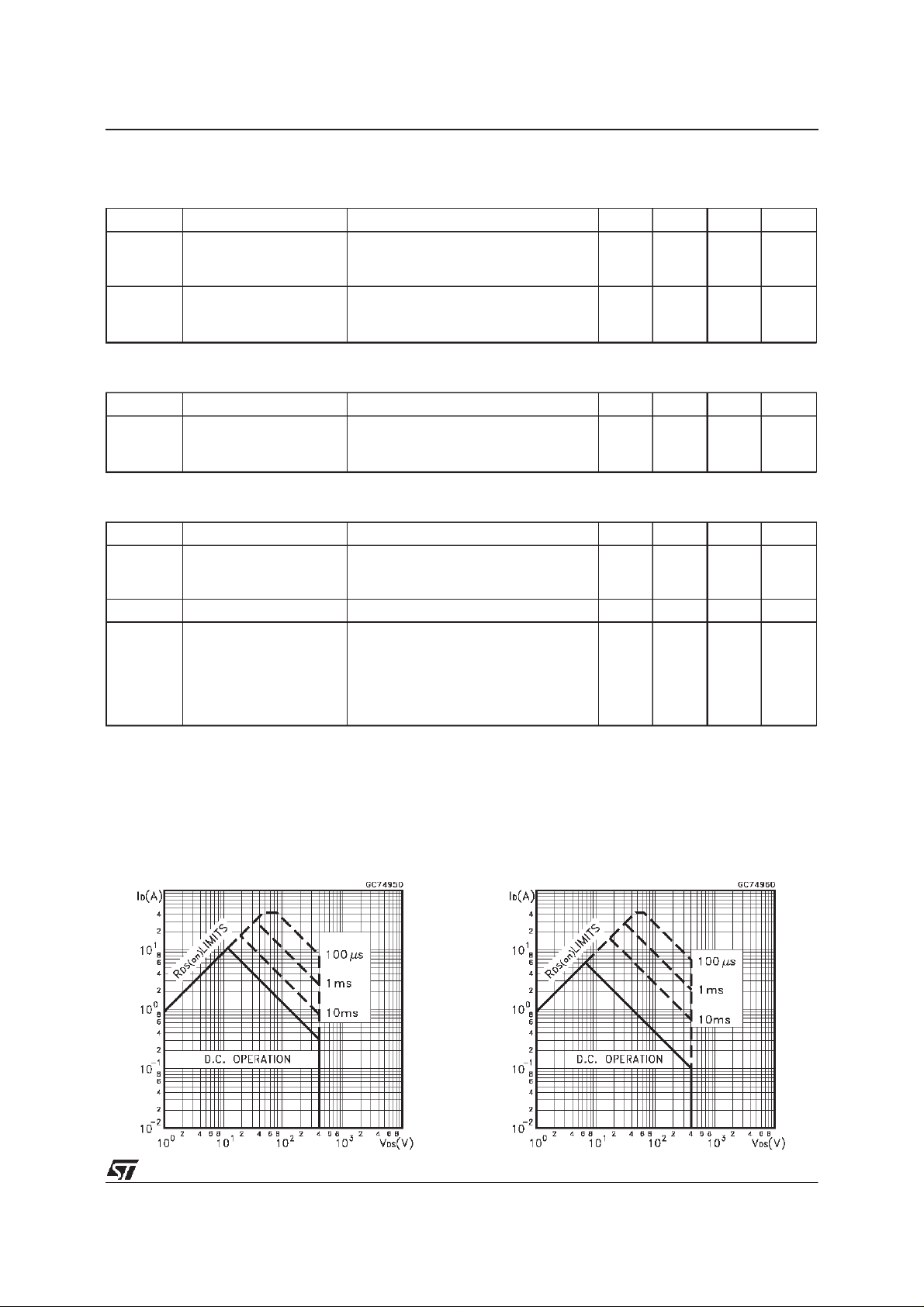
SafeOperating Area for TO-220 SafeOperating Area for TO-220FP
3/9
 Loading...