

查询STP10NB20供应商
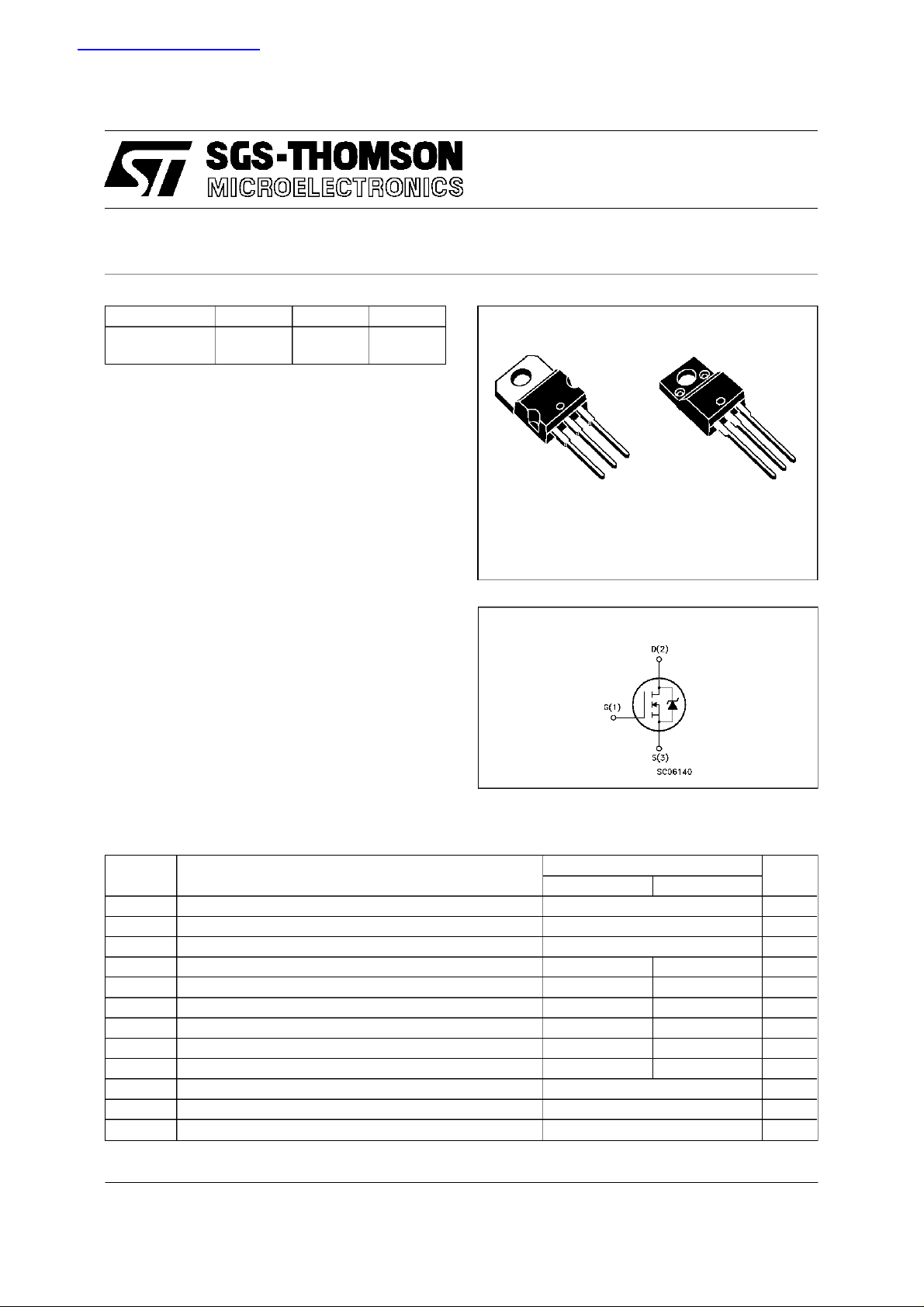
STP10NB20
STP10NB20FP
N - CHANNEL ENHANCEMENT MODE
PowerMESH MOSFET
TYPE V
STP10NB20
ST P10NB20FP
■ TYPICALR
■ EXTREMELY HIGH dv/dt CAPABILITY
■ 100% AVALANCHETESTED
■ VERYLOW INTRINSIC CAPACITANCES
■ GATECHARGEMINIMIZED
DS(on)
DSS
200 V
200 V
=0.3 Ω
R
DS(on)
<0.40Ω
<0.40Ω
I
D
10 A
6A
DESCRIPTION
Using the latest high voltage MESH OVERLAY
process, SGS-Thomson has designed an
advanced family of power MOSFETs with
outstanding performances. The new patent
pending strip layout coupled with the Company’s
proprietary edge termination structure, gives the
lowest RDS(on) per area, exceptional avalanche
and dv/dt capabilities and unrivalled gate charge
and switching characteristics.
APPLICATIONS
■ HIGH CURRENT, HIGHSPEEDSWITCHING
■ SWITCHMODEPOWER SUPPLIES(SMPS)
■ DC-ACCONVERTERS FOR WELDING
EQUIPMENTAND UNINTERRUPTIBLE
POWERSUPPLIESAND MOTORDRIVE
3
2
1
TO-220 TO-220FP
INTERNAL SCHEMATIC DIAGRAM
3
2
1
ABSOLUTE MAXIMUM RATINGS
Symbol Parameter Value Unit
ST P10 NB20 ST P1 0NB20FP
V
V
DGR
V
I
DM
P
dv/dt(
V
T
(•) Pulse width limited by safe operating area (1)ISD≤ 10A, di/dt ≤ 300 A/µs,VDD≤ V
November 1997
Drain-source Voltage (VGS=0) 200 V
DS
Drain- gate Voltage (RGS=20kΩ)
Gate-s ource Voltage ± 30 V
GS
Drain Curr ent ( con ti nuous) at Tc=25oC106A
I
D
Drain Curr ent ( con ti nuous) at Tc=100oC64A
I
D
200 V
(•) Dra in Curr ent (puls e d) 40 40 A
Total Dissipation at Tc=25oC8530W
tot
Derat ing F a c t or 0.68 0.24 W/
1) Peak Diode Rec overy volt ag e slope 5.5 5. 5 V/ ns
Ins ulation Withst and Voltage ( D C) 2000 V
ISO
Storage Temperature -65 to 150
stg
Max. Operating Junct ion Tempe r ature 150
T
j
(BR)DSS
,Tj≤T
JMAX
o
C
o
C
o
C
1/9
STP10NB20/FP
THERMAL DATA
TO-220 TO 220FP
R
thj-case
R
thj-amb
R
thc-sin k
T
AVALANCHE CHARACTERISTICS
Symbol Para met e r Max Value Uni t
I
AR
E
Ther mal Resist ance Junctio n-case M ax 1.47 4.17
Ther mal Resist ance Junctio n-ambient Max
Ther mal Resist ance Case-sink T yp
Maximum Lead Tem per a t ure For S oldering P urpose
l
Avalanche Cur rent, Repet it i v e or Not-Re petitive
(pulse width limited by T
Single Pulse Avalanche Energy
AS
(starting T
=25oC, ID=IAR,VDD=50V)
j
max, δ <1%)
j
62.5
0.5
300
10 A
150 mJ
o
C/W
o
C/W
o
C/W
o
C
ELECTRICAL CHARACTERISTICS (T
=25oC unlessotherwise specified)
case
OFF
Symbol Parameter Test Cond itions Min. Typ. Ma x. Unit
V
(BR)DSS
Drain-sourc e
=250µAVGS=0
I
D
200 V
Breakdown V oltage
I
I
DSS
GSS
Zer o Gat e V o lt age
Drain Current (V
GS
Gat e-body Leaka ge
Current (V
DS
=0)
=0)
=MaxRating
V
DS
V
=MaxRating Tc=125oC
DS
= ± 30 V
V
GS
1
10
± 100 nA
ON (∗)
Symbol Parameter Test Cond itions Min. Typ. Ma x. Unit
V
GS(th )
Gate Threshold
V
DS=VGSID
=250µA
345V
Voltage
R
DS(on)
Stati c D rain-source On
VGS=10V ID=5A 0.30 0.40 Ω
Resistance
I
D(on)
On State Drain Curre nt VDS>I
D(on)xRDS(on)max
10 A
VGS=10V
DYNAMIC
Symbol Parameter Test Cond itions Min. Typ. Ma x. Unit
g
(∗)Forward
fs
Tr ansconductanc e
C
C
C
Input Capac i t an c e
iss
Out put C apa c itance
oss
Reverse Transf er
rss
Capa cit an c e
VDS>I
D(on)xRDS(on)maxID
=5 A 3 4 S
VDS=25V f=1MHz VGS= 0 470
135
22
650
190
30
µA
µA
pF
pF
pF
2/9
STP10NB20/FP
ELECTRICAL CHARACTERISTICS (continued)
SWITCHINGON
Symbol Parameter Test Cond itions Min. Typ. Ma x. Unit
t
d(on)
t
r
Turn-on Time
Rise Tim e
VDD=100V ID=5A
=4.7 Ω VGS=10V
R
G
10
15
(see test circuit, figure 3)
Q
Q
Q
Total Gate Charge
g
Gat e-Sour ce Cha rge
gs
Gate-Drain Charge
gd
VDD=160V ID=10A VGS=10V 17
7.5
5.5
SWITCHINGOFF
Symbol Parameter Test Cond itions Min. Typ. Ma x. Unit
t
r(Voff)
t
t
Of f - voltage Rise Time
Fall Time
f
Cross-ov er Time
c
VDD=160V ID=10A
=4.7 Ω VGS=10V
R
G
(see test circuit, figure 5)
8
10
20
SOURCE DRAIN DIODE
Symbol Parameter Test Cond itions Min. Typ. Ma x. Unit
I
SD
I
SDM
V
SD
t
Q
I
RRM
(∗) Pulsed: Pulseduration = 300 µs, duty cycle 1.5 %
(•) Pulse width limited by safe operating area
Source-drain Curre nt
(•)
Source-drain Curre nt
(pulsed)
(∗) Forward On Voltage ISD=10 A VGS=0 1.5 V
Reverse Recov er y
rr
Time
Reverse Recov er y
rr
=10 A di/dt = 100 A /µs
I
SD
=50V Tj=150oC
V
DD
(see test circuit, figure 5)
170
980
Charge
Reverse Recov er y
11.5
Current
14
20
24 nC
11
14
28
10
40
ns
ns
nC
nC
ns
ns
ns
A
A
ns
nC
A
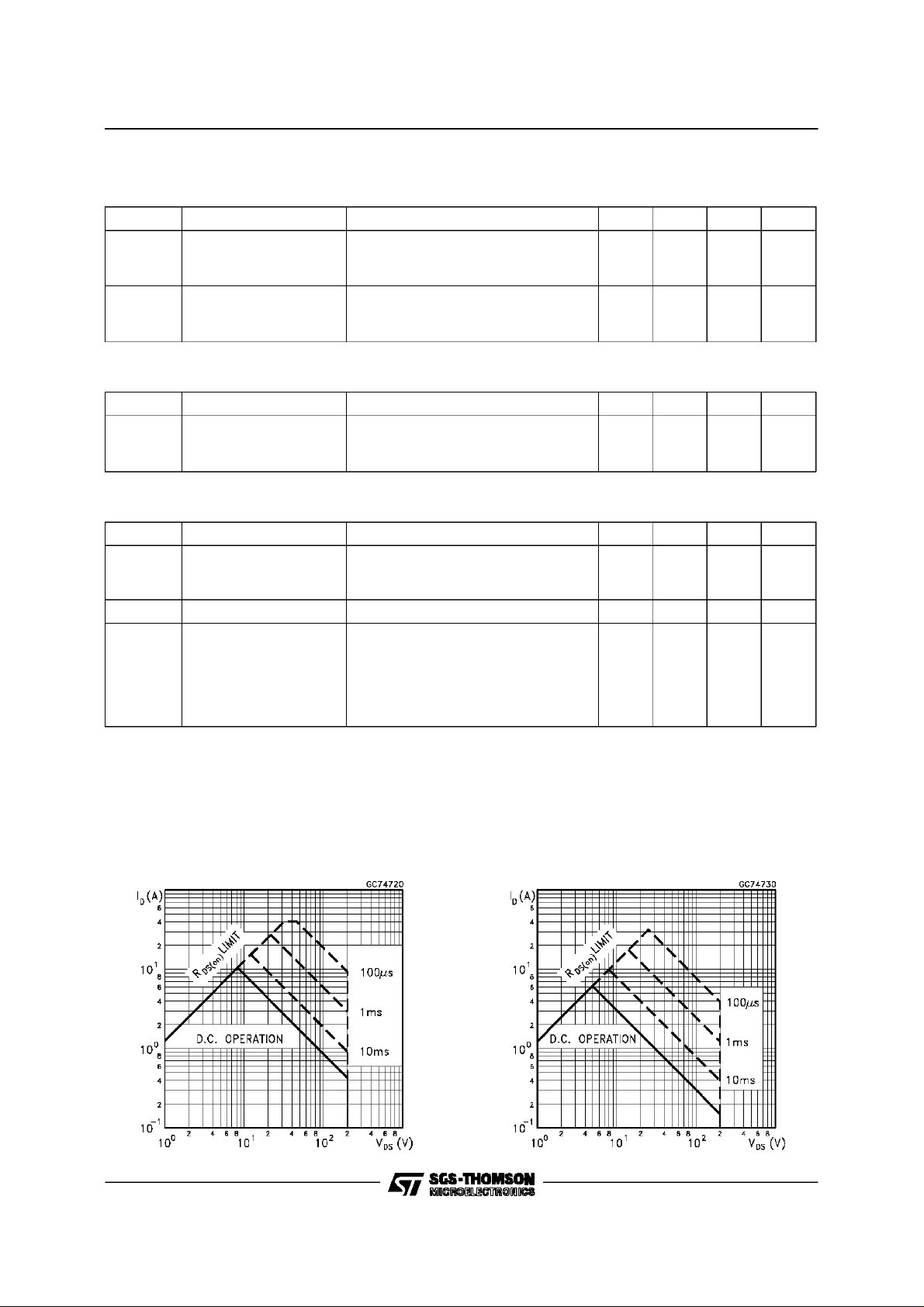
Safe Operating Area for TO-220 Safe Operating Area for TO-220FP
3/9
 Loading...