

4-bit constant current power-LED sink driver
Features
■ 4 constant current output channels
■ Adjustable output current through one external
resistor
■ Can be driven by a 3.3 V microcontroller
■ Serial data IN/parallel data OUT
■ Output current: 80-400 mA
■ 20 V of output driving capability
■ 30 MHz clock frequency
■ UVLO (under voltage lockout) and
POR (power ON reset)
■ TSD, thermal shutdown, output off when
junction temperature exceeds limit
■ Operating free-air temperature range -40° to
125 °C
■ ESD protection 2.5 kV HBM, 200 V MM
■ Available in high thermal TSSOP exposed pad.
STP04CM05
TSSOP16
(Exposed pad)
Description
The STP04CM05 is a high-power LED driver and
4-bit shift register designed for Power-LED
applications.
The STP04CM05 contains a 4-bit serial IN,
parallel OUT shift register that feeds a 4-bit
D-type storage register. In the output stage, four
regulated current sources were designed to
provide 80-400 mA constant current to drive high
power LEDs.
The STP04CM05 guarantees 20 V output driving
capability, allowing users to connect more LEDs in
series. The high clock frequency, 30 MHz, also
satisfies the system requirements which include
high volume data transmission.
SO-14
The STP04CM05 is well suited for very high
brightness displays and special lighting
applications.
The STP04CM05 is offered in SO-14 and
TSSOP16 exposed pad packages.
Table 1. Device summary
Order codes Package Packaging
STP04CM05MTR SO-14 (tape and reel) 2500 parts per reel
STP04CM05XTTR TSSOP16 exposed-pad (tape and reel) 2500 parts per reel
June 2010 Doc ID 14191 Rev 5 1/23
www.st.com
23

Contents STP04CM05
Contents
1 Internal schematic . . . . . . . . . . . . . . . . . . . . . . . . . . . . . . . . . . . . . . . . . . . 3
2 Pin settings . . . . . . . . . . . . . . . . . . . . . . . . . . . . . . . . . . . . . . . . . . . . . . . . 4
2.1 Pin connection . . . . . . . . . . . . . . . . . . . . . . . . . . . . . . . . . . . . . . . . . . . . . . 4
2.2 Pin description . . . . . . . . . . . . . . . . . . . . . . . . . . . . . . . . . . . . . . . . . . . . . . 4
3 Maximum rating . . . . . . . . . . . . . . . . . . . . . . . . . . . . . . . . . . . . . . . . . . . . . 5
3.1 Thermal data . . . . . . . . . . . . . . . . . . . . . . . . . . . . . . . . . . . . . . . . . . . . . . . 5
3.2 Recommended operating conditions . . . . . . . . . . . . . . . . . . . . . . . . . . . . . 6
4 Electrical characteristics . . . . . . . . . . . . . . . . . . . . . . . . . . . . . . . . . . . . . 7
5 Equivalent circuit of inputs and outputs . . . . . . . . . . . . . . . . . . . . . . . . . 9
6 Timing diagrams . . . . . . . . . . . . . . . . . . . . . . . . . . . . . . . . . . . . . . . . . . . 11
7 Test circuit . . . . . . . . . . . . . . . . . . . . . . . . . . . . . . . . . . . . . . . . . . . . . . . . 14
8 Typical characteristics . . . . . . . . . . . . . . . . . . . . . . . . . . . . . . . . . . . . . . 15
9 Package mechanical data . . . . . . . . . . . . . . . . . . . . . . . . . . . . . . . . . . . . 17
10 Revision history . . . . . . . . . . . . . . . . . . . . . . . . . . . . . . . . . . . . . . . . . . . 22
2/23 Doc ID 14191 Rev 5
STP04CM05 Internal schematic
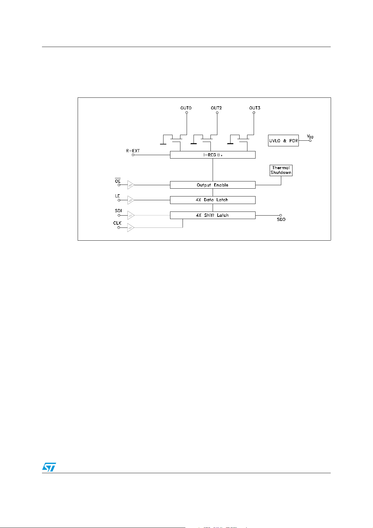
1 Internal schematic
Figure 1. Block diagram
Doc ID 14191 Rev 5 3/23
Pin settings STP04CM05
2 Pin settings
2.1 Pin connection
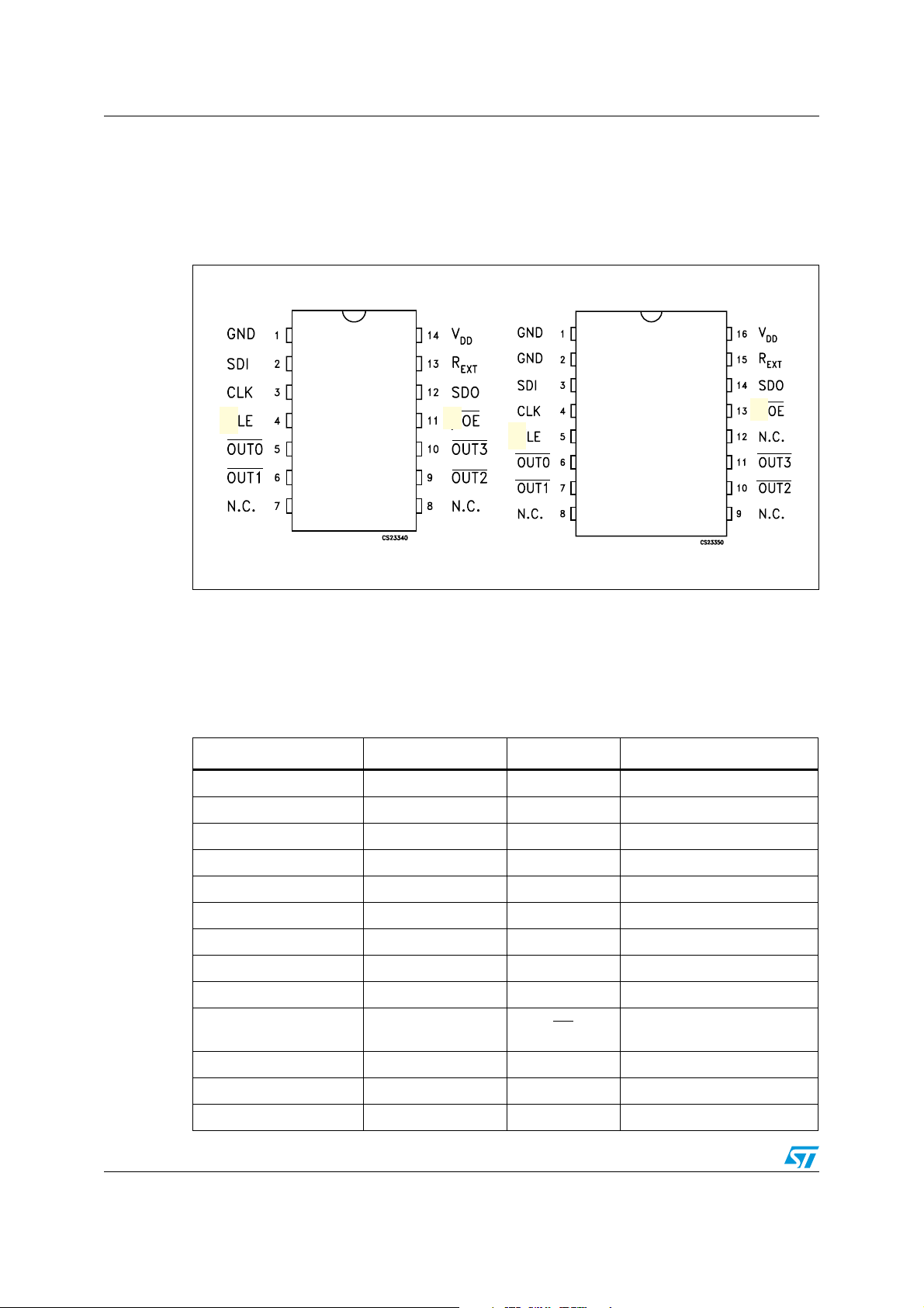
Figure 2. Pin connection
SO-14
TSSOP16 (exposed pad)
Note: The exposed pad should be electrically connected to a metal land electrically isolated or
connected to ground.
2.2 Pin description
Table 2. Pin description
SO-14 pin N° TSSOP16 pin N° Symbol Name and function
1 1, 2 GND Ground terminal
2 3 SDI Serial data input terminal
3 4 CLK Clock input terminal
4 5 LE Latch input terminal
5 6 OUT 0 Output terminal
6 7 OUT 1 Output terminal
7, 8 8, 9, 12 N.C. Not connected
9 10 OUT 2 Output terminal
10 11 OUT 3 Output terminal
11 13 OE
12 14 SDO Serial data out terminal
13 15 R-EXT Constant current programming
Output enable input terminal
(active low)
14 16 V
4/23 Doc ID 14191 Rev 5
DD
5 V supply voltage terminal
STP04CM05 Maximum rating
3 Maximum rating
Stressing the device above the rating listed in the “absolute maximum ratings” table may
cause permanent damage to the device. These are stress ratings only and operation of the
device at these or any other conditions above those indicated in the operating sections of
this specification is not implied. Exposure to absolute maximum rating conditions for
extended periods may affect device reliability.
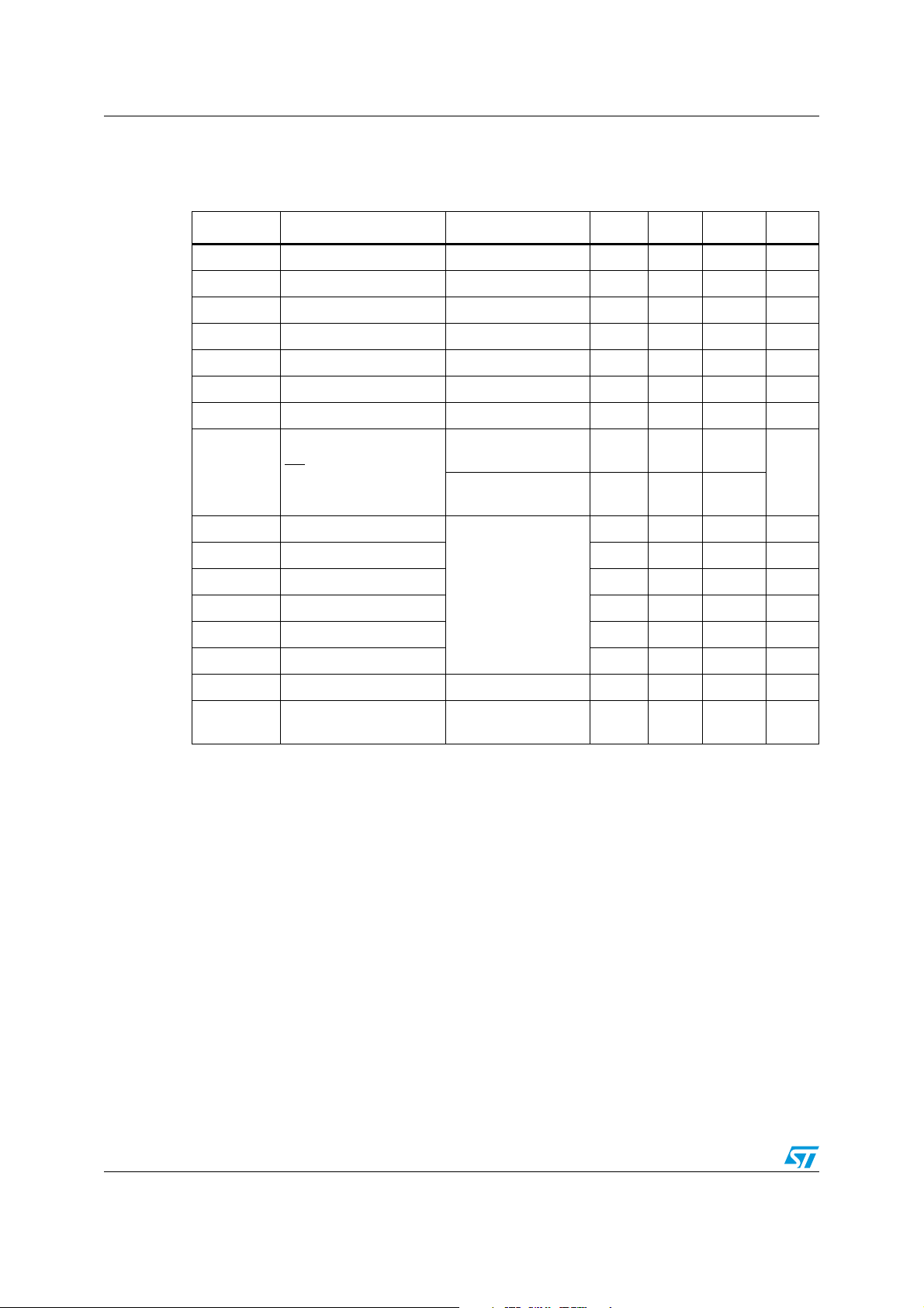
Table 3. Absolute maximum ratings
Symbol Parameter Value Unit
V
I
GND
f
T
T
V
CLK
OPR
Supply voltage 0 to 7 V
DD
Output voltage -0.5 to 20 V
O
I
Output current 500 mA
O
Input voltage -0.4 to VDD+0.4 V
V
I
GND terminal current 2000 mA
Clock frequency 50 MHz
Operating temperature range -40 to +125 °C
Storage temperature range -55 to +150 °C
STG
3.1 Thermal data
Table 4. Thermal data
Symbol Parameter SO-14 TSSOP16 Unit
R
thJA
1. 1 W of dissipated power, mounted on SM PCB1 SGS board
2. Using the PCB multi-layer JEDEC Standard test boards
Thermal resistance junction-ambient 105
(1)
37.5
(2)
°C/W
Doc ID 14191 Rev 5 5/23
Maximum rating STP04CM05
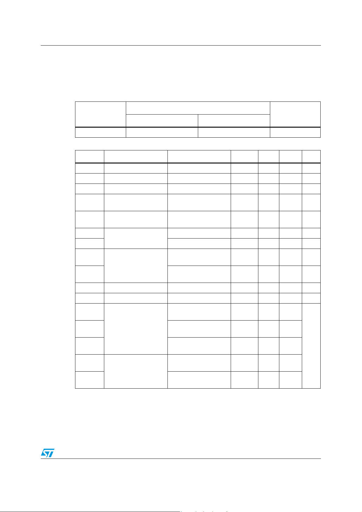
3.2 Recommended operating conditions
Table 5. Recommended operating conditions
Symbol Parameter Test conditions Min. Typ. Max. Unit
V
DD
V
O
I
O
I
OH
I
OL
V
IH
V
IL
t
wEN
t
wLAT
t
wCLK
t
SETUP(D)
t
HOLD(D)
t
SETUP(L)
t
HOLD(E)
f
CLK
T
OPR
1. If multiple devices are cascaded, it may not be possible achieve the maximum data transfer. Please
consider the timing conditions carefully.
Supply voltage 3.3 5.0 5.5 V
Output voltage 19 V
Output current OUTn V
= 5 V 80 400 mA
DD
Output current Serial-OUT +1 mA
Output current Serial-OUT -1 mA
Input voltage 0.7V
DD
Input voltage -0.3 0.3V
V
= 5 V,
DD
IO = 350 mA
80 50
VDD+0.3 V
DD
OE pulse width
= 3.3 V,
V
DD
IO = 350 mA
LE pulse width
250 150
84 ns
CLK pulse width 8.5 7.5 ns
Setup time for DATA 8.5 7.5 ns
= 3.0 to 3.6 V
V
Hold time for DATA 8.5 7.5 ns
DD
Setup time for LATCH 8.5 7.0 ns
Hold time for ENABLE 8.5 7.0 ns
Clock frequency Cascade operation
Operating temperature
range
(1)
-40 +125 °C
30 MHz
V
ns
6/23 Doc ID 14191 Rev 5
STP04CM05 Electrical characteristics
4 Electrical characteristics
TA = 25 °C, unless otherwise specified.
Table 6. Current accuracy
Current accuracy
Output voltage
Between bits Between ICs
≥ 1.4 V Typ. ± 1% ± 6% 80 to 400 mA
Table 7. Electrical characteristics (V
= 3.3 to 5 V)
DD
Symbol Parameter Test conditions Min. Typ. Max. Unit
Output current
V
IH
V
IL
I
OH
V
OL
V
OH
I
OL1
I
OL2
ΔI
OL1
ΔI
OL2
R
SIN(up)
R
SIN(down)
I
DD(OFF1)
I
DD(OFF2)
I
DD(OFF3)
Input voltage high level 0.7 V
DD
Input voltage low level GND 0.3 V
V
DD
DD
V
V
Output leakage current VOH = 19 V 10 μA
Output voltage
(Serial-OUT)
Output voltage
(Serial-OUT)
Output current
Output current error
= 1 mA 0.4 V
I
OL
= -1 mA VDD-0.4V V
I
OH
V
= 0.3 VR
O
VO = 1.2 VR
VO = 0.3 VR
IO = 80 mA
= 980 Ω 75.2 80 84.8 mA
EXT
= 190 Ω 376 400 424 mA
EXT
= 980 Ω
EXT
‘11.5%
between bit
(all output ON)
VO = 1.2 VR
= 400 mA
I
O
EXT
= 190 Ω
11.5%
Pull-up resistor 150 300 600 kΩ
Pull-down resistor 100 200 400 kΩ
= OPEN
R
Supply current (OFF)
EXT
OUT 0 to 3 = OFF
R
= 980 Ω
EXT
OUT 0 to 3 = OFF
R
= 190 Ω
EXT
OUT 0 to 3 = OFF
11.5
3.8 6
14 18.5
mA
I
DD(ON1)
I
DD(ON2)
Supply current (ON)
R
= 980 Ω
EXT
OUT 0 to 3 = ON
R
= 190 Ω
EXT
OUT 0 to 3 = ON
4.0 6.0
14.5 19
Doc ID 14191 Rev 5 7/23
 Loading...