

ST STOTG04ES User Manual
Feature summary
■ Meets the requirements of the universal serial
bus specification revision 2.0 And the on-thego supplement to the USB 2.0 specification
■ Analog car kit-compatible
■ Three operating modes: USB, UART and audio
■ Configurable using I
■ Capable of 12Mbit/s full-speed and 1.5Mbit/s
low-speed modes of operation
■ Standard digital interface compliant with the
OTG transceiver specification
■ Supports the session request protocol (SRP)
and host negotiation protocol (HNP)
■ 35mA Typical V
current for 3.3V supply voltage
■ Ability to control external charge pump for
higher V
■ Integrated pull-up/-down resistors
■ ±6kV ESD protection on all USB pins (contact
BUS
currents
discharge)
■ +1.6V to +3.6V Digital power supply and +2.7V
to +5.5V analog supply voltage range
■ Power-down mode with very low power
consumption for battery powered devices
■ Ideal for system ASICs with built-in USB OTG
dual role core
■ Available In QFN-24
■ –40°C to +85°C operating temperature range
2
C serial interface
Charge pump output
BUS
STOTG04ES
USB-OTG Full-speed Transceiver
QFN24 (4mmx4mm)
■ MP3 players
■ Digital cameras
■ Printers
Description
The STOTG04ES is a USB On-The-Go full-speed
transceiver. It provides complete physical layer
solution for any USB-OTG device. It contains
V
charge pump and comparators, ID line
BUS
detector and interrupt generator, and the USB
differential driver and receivers. The STOTG04
transceiver is suitable for mobile and battery
powered devices because of its low power
consumption and power down operating mode.
The transceiver is capable of operation in several
different modes. It can operate in basic USB-OTG
mode, as an UART transceiver or in audio mode.
Behavior of the transceiver is fully configurable
through the two-wire I
transceiver supports session request protocol and
host negotiation protocol.
2
C serial bus. The
Applications
■ Mobile phones
■ PDAs
Order code
Part number Package Packaging
STOTG04ESQTR QFN24 (4mm x 4mm) 4000 parts per reel
October 2006 Rev. 3 1/26
www.st.com
26

Contents STOTG04ES
Contents
1 Pin configuration . . . . . . . . . . . . . . . . . . . . . . . . . . . . . . . . . . . . . . . . . . . . . 3
2 Maximum ratings . . . . . . . . . . . . . . . . . . . . . . . . . . . . . . . . . . . . . . . . . . . . . . 5
3 Electrical characteristics . . . . . . . . . . . . . . . . . . . . . . . . . . . . . . . . . . . . . . . 6
4 Charge pump characteristics . . . . . . . . . . . . . . . . . . . . . . . . . . . . . . . . . . 10
5 Timing diagrams . . . . . . . . . . . . . . . . . . . . . . . . . . . . . . . . . . . . . . . . . . . . . 11
6 Block description . . . . . . . . . . . . . . . . . . . . . . . . . . . . . . . . . . . . . . . . . . . . 14
6.1 Charge pump . . . . . . . . . . . . . . . . . . . . . . . . . . . . . . . . . . . . . . . . . . . . . . . . 14
6.2 V
6.3 Voltage regulator . . . . . . . . . . . . . . . . . . . . . . . . . . . . . . . . . . . . . . . . . . . . . . 14
6.4 ID Line detector . . . . . . . . . . . . . . . . . . . . . . . . . . . . . . . . . . . . . . . . . . . . . . . 14
6.5 Driver and receivers . . . . . . . . . . . . . . . . . . . . . . . . . . . . . . . . . . . . . . . . . . . 14
6.6 Control logic . . . . . . . . . . . . . . . . . . . . . . . . . . . . . . . . . . . . . . . . . . . . . . . . . 15
6.7 Modes of operation . . . . . . . . . . . . . . . . . . . . . . . . . . . . . . . . . . . . . . . . . . . . 15
6.8 Registers . . . . . . . . . . . . . . . . . . . . . . . . . . . . . . . . . . . . . . . . . . . . . . . . . . . . 17
6.9 I
6.10 Device address . . . . . . . . . . . . . . . . . . . . . . . . . . . . . . . . . . . . . . . . . . . . . . . 19
6.11 Bus protocol . . . . . . . . . . . . . . . . . . . . . . . . . . . . . . . . . . . . . . . . . . . . . . . . . 19
6.12 External charge pump switch . . . . . . . . . . . . . . . . . . . . . . . . . . . . . . . . . . . . 21
Comparators . . . . . . . . . . . . . . . . . . . . . . . . . . . . . . . . . . . . . . . . . . . . 14
BUS
6.7.1 Power modes . . . . . . . . . . . . . . . . . . . . . . . . . . . . . . . . . . . . . . . . . . . . . . . . . 15
6.7.2 USB Modes . . . . . . . . . . . . . . . . . . . . . . . . . . . . . . . . . . . . . . . . . . . . . . . . . . 15
6.7.3 UART Mode . . . . . . . . . . . . . . . . . . . . . . . . . . . . . . . . . . . . . . . . . . . . . . . . . . 16
6.7.4 Audio mode . . . . . . . . . . . . . . . . . . . . . . . . . . . . . . . . . . . . . . . . . . . . . . . . . . 17
2
C Bus interface . . . . . . . . . . . . . . . . . . . . . . . . . . . . . . . . . . . . . . . . . . . . . . 19
7 Package mechanical data . . . . . . . . . . . . . . . . . . . . . . . . . . . . . . . . . . . . . . 22
8 Revision history . . . . . . . . . . . . . . . . . . . . . . . . . . . . . . . . . . . . . . . . . . . . . . 25
2/26
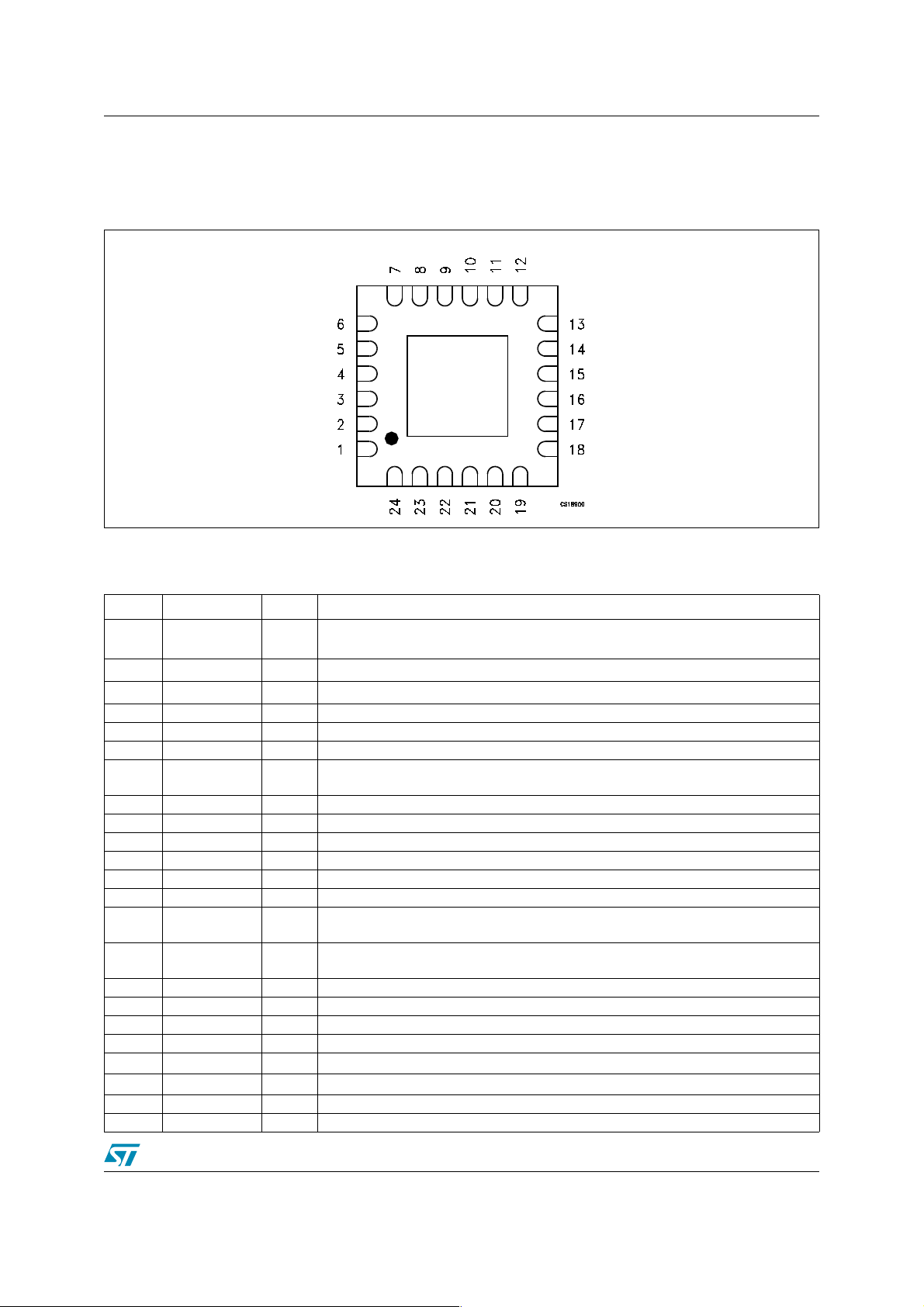
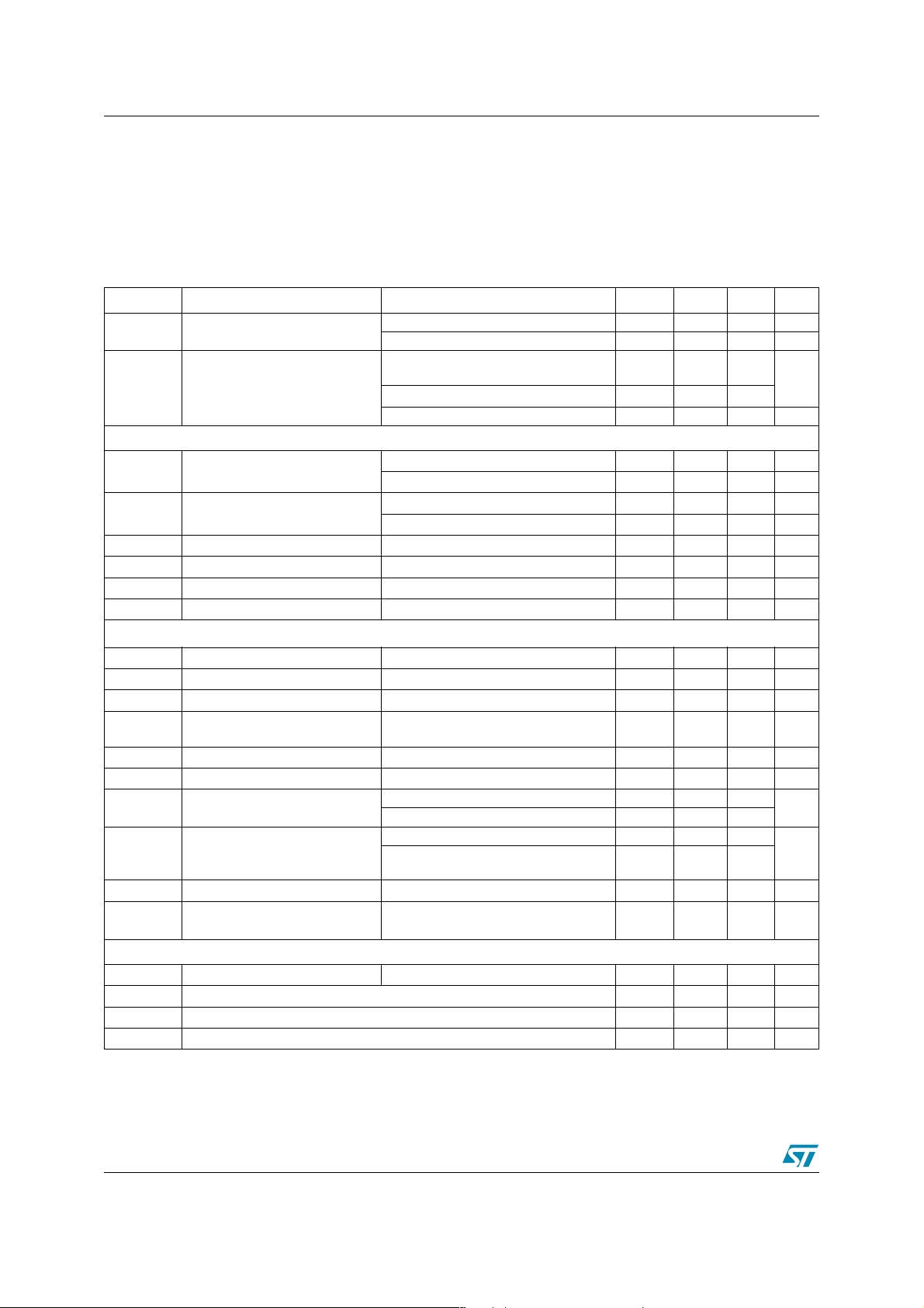
STOTG04ES Pin configuration
1 Pin configuration
Figure 1. Pin connections (bottom view )
Table 1. Pin description
PlN N° SYMBOL I/O NAME AND FUNCTION
2
1 ADR_PSW I/O
2 SDA I/O
3SCLI
4 RESET/ I Active low logic reset
5 INT/ O Active low interrupt signal (open-drain)
6 SPEED I Mode of the transceiver (0 = low-speed, 1 = full-speed) (2)
7
8 SUSPEND I Power down input (0 = active mode, 1 = power down) (See
9 OE_TP_INT/ I/O Output enable of the differential driver in the USB mode or interrupt output
10 VM O D– single-ended receiver output
11 VP O D+ single-ended receiver output
12 RCV O Differential receiver output
13 SE0_VM I/O
14 DAT_VP I/O
15 D- I/O Negative data line in the USB mode or serial data output in the UART mode
16 D+ I/O Positive data line in the USB mode or serial data input in the UART mode
17 GND Power Common analog and digital ground
18 ID I/O ID pin of the USB connector used for protocol identification
19
20
21 CAP1 I/O External capacitor pin for the charge pump
22 CAP2 I/O External capacitor pin for the charge pump
V
TRM
ExpPad - Not Connected
V
BUS
V
BAT
Power
Power Analog power supply voltage (+2.7V to +5.5V)
Least significant bit of the I
PSW output enabling or disabling an external charge pump
2
C serial data (1)
I
I2C clock
Internal voltage regulator output; an external decoupling capacitor should be
connected (3)
Single-ended zero input/output in the DAT_SE0 mode transmit mode, negative
data input/output in the single-ended transmit mode or TXD in the UART mode
Data input/output in the DAT_SE0 mode transmit mode, positive data input/
output in the single-ended transmit mode or RXD in the UART mode
line of the USB interface – it needs an external capacitor of 4.7µF
V
I/O
BUS
C address of the transceiver input latched on reset;
Ta bl e 8
)
3/26
Pin configuration STOTG04ES
PlN N° SYMBOL I/O NAME AND FUNCTION
23 CGND Power Ground for the charge pump
24
(1) Input and open-drain output
(2) Input with internal pull-up resistor
(3) Internal regulator can be bypassed by connecting V
V
IF
Power Logic power supply (+1.6V to 3.6V)
to this pin when the V
BAT
is in range of 2.7V to 3.6V
BAT
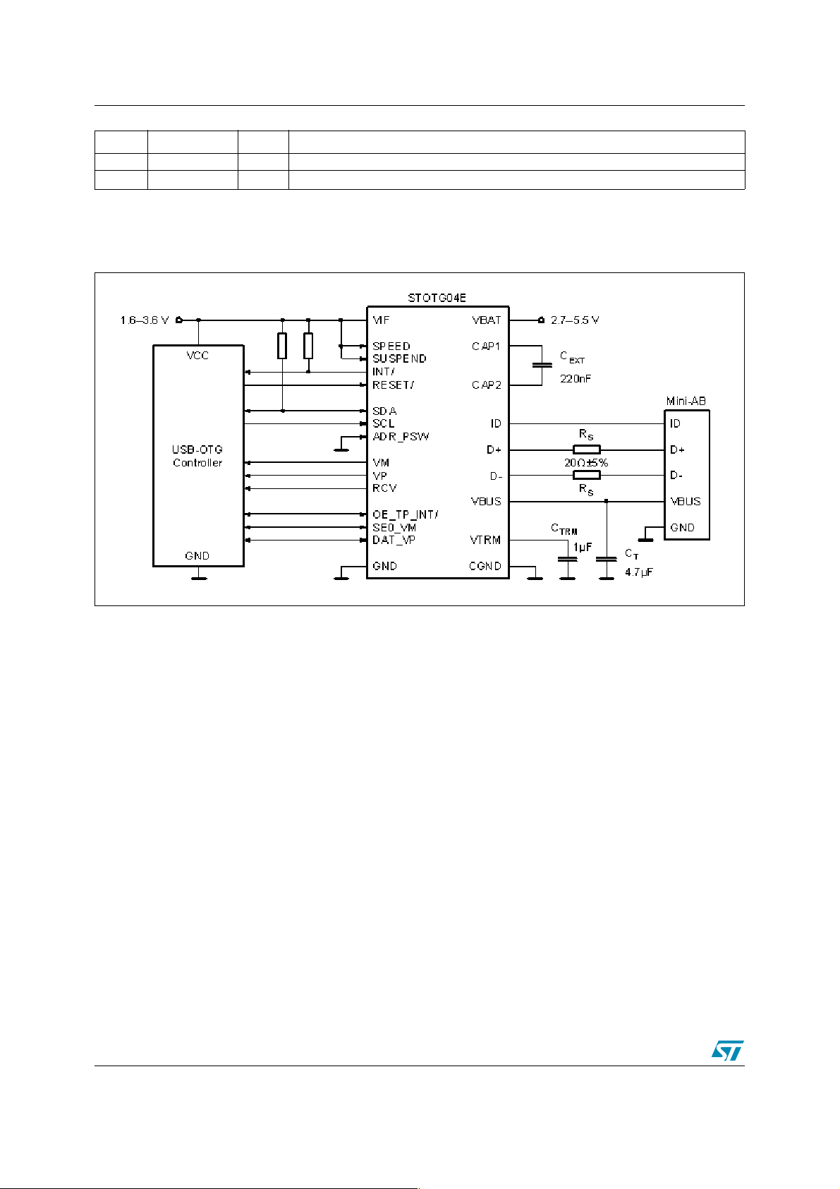
Figure 2. Functional diagram
4/26
STOTG04ES Maximum ratings
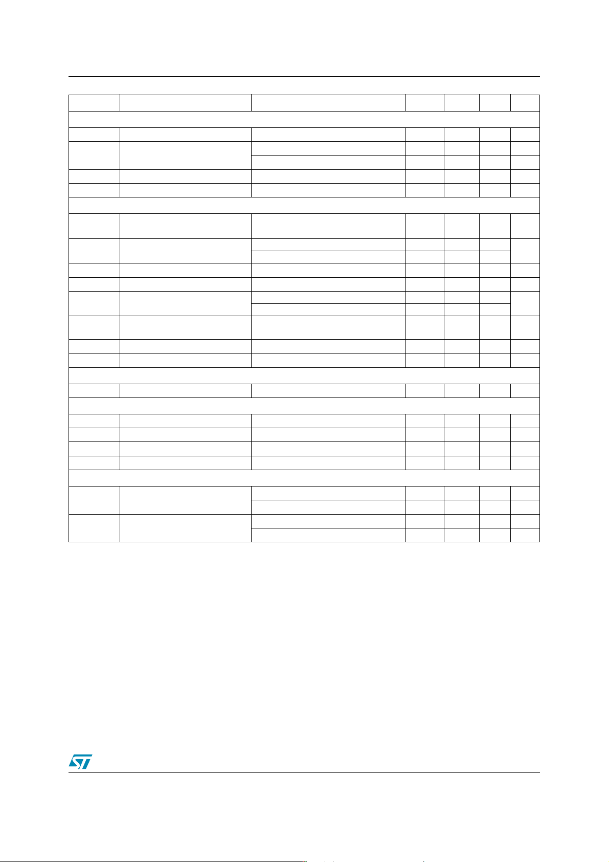
2 Maximum ratings
Table 2. Absolute maximum ratings
Symbol Parameter Value Unit
V
V
BAT
V
DCDIG
T
STG
V
ESD
(*) In accordance to IEC61000-4-2, level 3.
Absolute Maximum Ratings are those values beyond which damage to the device may occur. Functional Operation under these con-
ditions is not implied.
Table 3. Thermal data
Symbol Parameter Value Unit
R
thJA
Table 4. Recommended operating condition
Symbol Parameter Min. Typ. Max. Unit
V
V
BAT
T
C
EXT
C
C
TRM
R
Logic Supply Voltage -0.5 to + 4.5 V
IF
Analog Supply Voltage -0.5 to + 6.5 V
DC Input Voltage on any logic interface pin -0.5 to + 4.5 V
Storage Temperature Range -65 to + 150 °C
Electrostatic discharge voltage
on USB pins
Human Body Model ± 8
Contact Discharge (*) ± 6
Thermal Resistance Junction-Ambient 59 °C/W
Logic Supply Voltage 1.6 1.8 3.6 V
IF
Analog Supply Voltage 2.7 3.3 5.5 V
Operating Temperature Range -40 +85 °C
A
Charge pump external capacitor 100 220 470 nF
Charge pump tank capacitor 1 4.7 6.5 µF
T
Voltage regulator external capacitor 1 µF
Data lines impedance matching resistor 20 Ω
S
kV
Table 5. ESD Performance
Symbol Parameter Value Unit
IEC-61000-4-2 (D+, D-, VBUS, ID)
ESD
IEC-61000-4-2 (other pins)
Air discharge (10 pulses) ± 8
Contact discharge (10 pulses) ± 6
Air discharge (10 pulses) ± 2
Contact discharge (10 pulses) ± 2
kV
5/26
Electrical characteristics STOTG04ES
3 Electrical characteristics
Table 6. Electrical characteristics
Characteristics measured over recommended operating conditions unless otherwise is
noted. All typical values are referred to T
C
= 220nF, CT = 4.7µF and C
EXT
Symbol Parameter Test Conditions Min. Typ. Max. Unit
I
BAT
I
Digital Part Supply Current
IF
Operating Supply Current
LOGIC INPUTS AND OUTPUTS
V
V
V
V
I
LKG
I
OZ
V
BUS
V
BUS
V
BUS_LKGVBUS
V
BUS_RIPVBUS
f
CP
R
VBUSVBUS
I
VBUS
V
BUS_VLD
HIGH level output voltage
OH
LOW level output voltage
OL
HIGH level input voltage
IH
LOW level input voltage
IL
Input leakage current -1 1 µA
Off-state output current -5 5 µA
V
output voltage I
BUS
leakage voltage
output ripple I
Charge-pump switching
frequency (2)
input impedance
Maximum V
V
valid comparator
BUS
source current C
BUS
threshold
Session valid comparator
V
SES_VLD
threshold for both A and B
devices
R
VBUS_PUVBUS
R
VBUS_PD
charge pull-up resistance
V
discharge pull-down
BUS
resistance
ID
V
ID_BIAS
R
ID_PU
R
ID_GND
R
ID_FLOAT
ID pin bias voltage
ID pin pull-up resistance 70 105 130 kΩ
ID line short resistance to detect id_gnd state 10 Ω
ID line short resistance to detect id_float state 800 kΩ
TRM
Active mode (1,2) 0.6 1.6 mA
Power down mode 1 µA
Transceiver current while
transmitting and receiving (1,2)
Charge pump current, I
Power down mode (3) 1 µA
= -100µA VIF-0.15
I
OH
I
= -2mA VIF-0.40
OH
= 100µA
I
OL
I
= 2mA
OL
= 8mA
LOAD
No Load 3 200 mV
= 8mA, CT = 4.7µF
LOAD
= 220 nF, V
EXT
Low to high transition 4.40
High to low transition 4.40
Low to high transition 0.8 2.0
High to low transition 0.8 2.0
= 140kΩ, V
R
CP_ID
= 25°C, VIF = 1.8V, V
A
= 1µF
LOAD
> 4.4V
BUS
≤ 5V
BAT
= 8mA
= 3.3V, RS = 20Ω,
BAT
4.5 7
17 25
0.15 V
0.40 V
0.7V
IF
0.3V
IF
4.4 4.9 5.25 V
30 60 mV
0.5 0.8 1.5 MHz
40 76 100 kΩ
20 35 mA
281 640 Ω
656 1260 Ω
1.3 1.9 3.0 V
mA
V
V
V
V
V
V
6/26
STOTG04ES Electrical characteristics
Symbol Parameter Test Conditions Min. Typ. Max. Unit
DIFFERENTIAL DRIVER
Z
DRV
V
OH_DRV
V
OL_DRV
V
CRS
Output Impedance
HIGH level output voltage
LOW level output voltage
Driver crossover voltage
DIFFERENTIAL AND SINGLE-ENDED RECEIVERS
V
V
SE-TH
R
C
R
PU_D+
R
PU_D-
R
V
DT_LKG
Differential receiver input
DI
sensitivity (V
D+
- VD-)
SE receivers switching
threshold
Input resistance PU/PD resistor deactivated 1.5 MΩ
IN
Input capacitance 10 30 pF
IN
Data line pull-up resistance on
pin D+
Data line pull-up resistance on
pin D-
Data line pull-down resistance 14.25 17.0 24.8 kΩ
PD
Data line leakage voltage
CAR KIT INTERRUPT DETECTOR
V
CR_INT_TH
Car kit Interrupt threshold 0.4 0.6 V
UART MODE – D+ AND D- PINS
V
V
V
V
HIGH level output voltage
OH
LOW level output voltage
OL
HIGH level input voltage 2.0 V
IH
LOW level input voltage 0.8 V
IL
VOLTAGE REGULATOR
V
TRM
I
TRM
(1) Transmitting and receiving at 12Mbit/s, loads of 50pF on D+ and D- pins, no capacitive loads on VP and VM pins
(2) Not tested in production; characterization only
(3) See paragraph 6.7.1
Internal power supply voltage
Voltage regulator output
current
Excluding external R
= 14.25kΩ, V
R
LH
RLH = 14.25kΩ, V
= 1.425kΩ
R
LL
= 50 to 600pF
C
LOAD
= 0.8 to 2.5V
V
CM
TRM
TRM
S
= 3.3V
= 2.7V
81624Ω
2.8 3.6 V
2.6 3.0 V
00.3V
1.3 1.67 2.0 V
-200 200 mV
Low to high transition 0.8 1.6 2.0
High to low transition 0.8 1.1 2.0
Bus Idle 900 1300 1575
Receiving mode 1425 2200 3090
900 1300 1575 Ω
R
I
I
V
V
V
V
OH
OL
= 300kΩ
PU_EXT
= -2mA
= 2mA
= 3.3 to 5V, no load; uart_en=0
BAT
= 2.8 to 5V, no load; uart_en=1
BAT
= 3.6V, V
BAT
= 3.0V, V
BAT
> 3V; uart_en=0
TRM
>2.6V; uart_en=1
TRM
200 342 mV
2.4 3.6 V
00.4V
3.0 3.3 3.6 V
2.6 2.75 2.9 V
20 mA
10 mA
V
Ω
7/26
Electrical characteristics STOTG04ES
Table 7. Switching characteristics
Over recommended operating conditions unless otherwise is noted. All the typical values are
referred to T
= 1µF
C
TRM
Symbol Parameter Test Conditions Min. Typ. Max. Unit
T
VBUS_RISEVBUS
DIFFERENTIAL DRIVER
t
R
t
F
t
P_DRV_R
t
P_DRV_F
t
RFM
SINGLE-ENDED RECEIVERS
t
P_SE_R
t
P_SE_F
DIFFERENTIAL RECEIVER
t
P_DIF_R
t
P_DIF_F
DIGITAL INTERFACE
t
SET_OE
t
TA _ OI
t
TA _ IO
I2C BUS (3)
f
SCL
t
LOW
t
HIGH
t
IICR
rise time I
Data signal rise time
Data signal rise time
Propagation delay of the driver,
rising edge; DAT_SE0 mode
Propagation delay of the driver,
rising edge; VP_VM mode
Propagation delay of the driver,
falling edge; DAT_SE0 mode
Propagation delay of the driver,
rising edge; VP_VM mode
Rise and fall time matching (tR/
tF) excluding the first transition
from the idle state
Propagation delay of the SE
receiver, rising edge
Propagation delay of the SE
receiver, falling edge
Propagation delay of the SE
receiver, rising edge
Propagation delay of the SE
receiver, falling edge
Output enable setup time 50 ns
Output to input bus turnaround
time (1, 2)
Output to input bus turnaround
time (1, 2)
SCL clock frequency 100 kHz
Low period of the SCL clock 4.7 µs
High period of the SCL clock 4.0 µs
Rise time of both SDA and SCL
signals
= 25°C, VIF = 1.8V, V
A
LOAD
Full-speed mode, C
Low-speed mode, C
Full-speed mode, C
Low-speed mode, C
Full-speed mode, C
Low-speed mode, C
Full-speed mode, C
Low-speed mode, C
Full-speed mode, C
Low-speed mode, C
Full-speed mode, C
Low-speed mode, C
Full-speed mode 90 111.11
Low-speed mode 80 125
Full-speed mode, input slope 15ns 18
Low-speed mode, input slope
150ns
Full-speed mode, input slope 15ns 18
Low-speed mode, input slope
150ns
Full-speed mode, input slope 15ns 24
Low-speed mode, input slope
150ns
Full-speed mode, input slope 15ns 24
Low-speed mode, input slope
150ns
= 3.3V, RS = 20Ω, C
BAT
= 8mA, CT = 10µF
LOAD
LOAD
LOAD
LOAD
LOAD
LOAD
LOAD
LOAD
LOAD
LOAD
LOAD
LOAD
= 50pF
= 600pF
= 50pF
= 600pF
= 50pF
= 600pF
= 50pF
= 600pF
= 50pF
= 600pF
= 50pF
= 600pF
= 220nF, CT = 4.7µF, and
EXT
1100ms
48.520
75 110 300
48.520
75 110 300
38
280
55
300
38
280
55
300
ns
ns
ns
ns
ns
ns
%
18
18
24
24
ns
ns
ns
ns
05ns
05ns
1000 ns
8/26
 Loading...