

Smart push-button on/off controller with Smart Reset™ and
Features
■ Operating voltage 1.6 V to 5.5 V
■ Low standby current of 0.6 µA
■ Adjustable Smart Reset
driven by external C
■ Power-up duration determined primarily by
push-button press (STM6600) or by fixed time
period, t
■ Debounced PB and SR inputs
■ PB and SR ESD inputs withstand voltage up to
ON_BLANK
±15 kV (air discharge) ±8 kV (contact
discharge)
■ Active high or active low enable output option
(EN
or EN) provides control of MOSFET,
DC-DC converter, regulator, etc.
■ Secure startup, interrupt, Smart Reset
power-down driven by push-button
■ Precise 1.5 V voltage reference with 1%
accuracy
■ Industrial operating temperature –40 to +85 °C
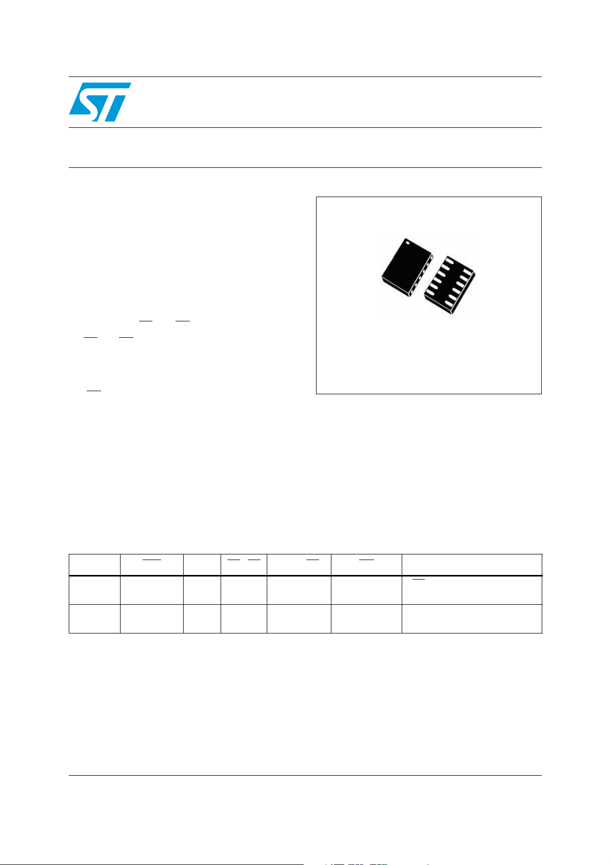
■ Available in TDFN12 2 x 3 mm package
™
assertion delay time
SRD
(STM6601)
™
or
STM6600, STM6601
power-on lockout
Datasheet − production data
TDFN12
Applications
■ Portable devices
■ Termin
■
A
■ Cell phones and smart phones
■ PDAs, palmtops, organizers
als
udio and video players
Table 1. Device summary
Device RST C
STM6600 open drain
STM6601 open drain
1. External pull-up resistor needs to be connected to open drain outputs.
2. For a successful startup, the PS
(1)
(1)
June 2012 Doc ID 15453 Rev 11 1/52
This is information on a product in full production.
PB / SR EN or EN INT Startup process
SRD
PB must be held low until the
✓✓push-pull open drain
✓✓push-pull open drain
(Power Supply Hold) needs to be pulled high within specific time, t
HOLD
(1)
(1)
PS
HOLD
PB can be released before the
PS
HOLD
(2)
confirmation
(2)
confirmation
ON_BLANK
.
www.st.com
1

Contents STM6600, STM6601
Contents
1 Description . . . . . . . . . . . . . . . . . . . . . . . . . . . . . . . . . . . . . . . . . . . . . . . . . 5
2 Pin descriptions . . . . . . . . . . . . . . . . . . . . . . . . . . . . . . . . . . . . . . . . . . . . 9
3 Operation . . . . . . . . . . . . . . . . . . . . . . . . . . . . . . . . . . . . . . . . . . . . . . . . . 12
4 Waveforms . . . . . . . . . . . . . . . . . . . . . . . . . . . . . . . . . . . . . . . . . . . . . . . . 14
5 Typical operating characteristics . . . . . . . . . . . . . . . . . . . . . . . . . . . . . 28
6 Maximum ratings . . . . . . . . . . . . . . . . . . . . . . . . . . . . . . . . . . . . . . . . . . . 38
7 DC and AC characteristics . . . . . . . . . . . . . . . . . . . . . . . . . . . . . . . . . . . 39
8 Package mechanical data . . . . . . . . . . . . . . . . . . . . . . . . . . . . . . . . . . . . 42
9 Part numbering . . . . . . . . . . . . . . . . . . . . . . . . . . . . . . . . . . . . . . . . . . . . 46
10 Product selector . . . . . . . . . . . . . . . . . . . . . . . . . . . . . . . . . . . . . . . . . . . 49
11 Revision history . . . . . . . . . . . . . . . . . . . . . . . . . . . . . . . . . . . . . . . . . . . 51
2/52 Doc ID 15453 Rev 11

STM6600, STM6601 List of tables
List of tables
Table 1. Device summary. . . . . . . . . . . . . . . . . . . . . . . . . . . . . . . . . . . . . . . . . . . . . . . . . . . . . . . . . . 1
Table 2. Pin descriptions . . . . . . . . . . . . . . . . . . . . . . . . . . . . . . . . . . . . . . . . . . . . . . . . . . . . . . . . . . 7
Table 3. Absolute maximum ratings . . . . . . . . . . . . . . . . . . . . . . . . . . . . . . . . . . . . . . . . . . . . . . . . . 38
Table 4. Operating and AC measurement conditions . . . . . . . . . . . . . . . . . . . . . . . . . . . . . . . . . . . . 39
Table 5. DC and AC characteristics . . . . . . . . . . . . . . . . . . . . . . . . . . . . . . . . . . . . . . . . . . . . . . . . . 39
Table 6. TDFN12 (2 x 3 mm) package mechanical data . . . . . . . . . . . . . . . . . . . . . . . . . . . . . . . . . 43
Table 7. Carrier tape dimensions for TDFN12 (2 x 3 mm) package . . . . . . . . . . . . . . . . . . . . . . . . . 45
Table 8. STM6600 ordering information scheme . . . . . . . . . . . . . . . . . . . . . . . . . . . . . . . . . . . . . . . 46
Table 9. STM6601 ordering information scheme . . . . . . . . . . . . . . . . . . . . . . . . . . . . . . . . . . . . . . . 48
Table 10. STM6600 product selector . . . . . . . . . . . . . . . . . . . . . . . . . . . . . . . . . . . . . . . . . . . . . . . . . 49
Table 11. STM6601 product selector . . . . . . . . . . . . . . . . . . . . . . . . . . . . . . . . . . . . . . . . . . . . . . . . . 50
Table 12. Document revision history . . . . . . . . . . . . . . . . . . . . . . . . . . . . . . . . . . . . . . . . . . . . . . . . . 51
Doc ID 15453 Rev 11 3/52

List of figures STM6600, STM6601
List of figures
Figure 1. Application hookup . . . . . . . . . . . . . . . . . . . . . . . . . . . . . . . . . . . . . . . . . . . . . . . . . . . . . . . 5
Figure 2. Basic functionality (option with enable deassertion after long push) . . . . . . . . . . . . . . . . . . 6
Figure 3. Basic functionality (option with RST
Figure 4. Logic diagram . . . . . . . . . . . . . . . . . . . . . . . . . . . . . . . . . . . . . . . . . . . . . . . . . . . . . . . . . . . . 6
Figure 5. TDFN12 pin connections . . . . . . . . . . . . . . . . . . . . . . . . . . . . . . . . . . . . . . . . . . . . . . . . . . . 7
Figure 6. Block diagram . . . . . . . . . . . . . . . . . . . . . . . . . . . . . . . . . . . . . . . . . . . . . . . . . . . . . . . . . . . . 8
Figure 7. Successful power-up on STM6600 (PB
Figure 8. Successful power-up on STM6600 (t
Figure 9. Unsuccessful power-up on STM6600 (PB
Figure 10. Unsuccessful power-up on STM6600 (t
Figure 11. Successful power-up on STM6601. . . . . . . . . . . . . . . . . . . . . . . . . . . . . . . . . . . . . . . . . . . 18
Figure 12. Unsuccessful power-up on STM6601
Figure 13. Power-up on STM660x with voltage dropout . . . . . . . . . . . . . . . . . . . . . . . . . . . . . . . . . . . 20
Figure 14. PB
Figure 15. Long push, PB
Figure 16. Long push, SR
interrupt. . . . . . . . . . . . . . . . . . . . . . . . . . . . . . . . . . . . . . . . . . . . . . . . . . . . . . . . . . . . . 21
pressed first . . . . . . . . . . . . . . . . . . . . . . . . . . . . . . . . . . . . . . . . . . . . . . . . 22
pressed first . . . . . . . . . . . . . . . . . . . . . . . . . . . . . . . . . . . . . . . . . . . . . . . . 22
Figure 17. Invalid long push . . . . . . . . . . . . . . . . . . . . . . . . . . . . . . . . . . . . . . . . . . . . . . . . . . . . . . . . 23
Figure 18. Long push (option with RST
assertion). . . . . . . . . . . . . . . . . . . . . . . . . . . . . . . . . . . . . . . . 24
Figure 19. Long push (option with enable deassertion) . . . . . . . . . . . . . . . . . . . . . . . . . . . . . . . . . . . 25
Figure 20. Undervoltage detected for <t
Figure 21. Undervoltage detected for >t
Figure 22. PB
output waveform . . . . . . . . . . . . . . . . . . . . . . . . . . . . . . . . . . . . . . . . . . . . . . . . . . . 27
OUT
SRD
SRD
Figure 23. Supply current vs. temperature, normal state. . . . . . . . . . . . . . . . . . . . . . . . . . . . . . . . . . . 28
Figure 24. Supply current vs. temperature, standby state . . . . . . . . . . . . . . . . . . . . . . . . . . . . . . . . . . 28
Figure 25. Supply current vs. supply voltage, normal state . . . . . . . . . . . . . . . . . . . . . . . . . . . . . . . . . 29
Figure 26. Supply current vs. supply voltage, standby state . . . . . . . . . . . . . . . . . . . . . . . . . . . . . . . . 29
Figure 27. Threshold vs. temperature, V
Figure 28. Threshold hysteresis vs. temperature, V
Figure 29. Debounce period vs. supply voltage . . . . . . . . . . . . . . . . . . . . . . . . . . . . . . . . . . . . . . . . . . 31
Figure 30. C
charging current vs. temperature, VCC = 3.6 V . . . . . . . . . . . . . . . . . . . . . . . . . . . . . 31
SRD
Figure 31. Output low voltage vs. output low current, T
Figure 32. Output high voltage vs. output high current, T
Figure 33. Output voltage vs. supply voltage, I
Figure 34. Input voltage vs. temperature . . . . . . . . . . . . . . . . . . . . . . . . . . . . . . . . . . . . . . . . . . . . . . . 33
Figure 35. Reference output voltage vs. temperature, V
Figure 36. Reference output voltage vs. load current, V
Figure 37. Reference output voltage vs. supply voltage, T
Figure 38. Reference startup, I
= 15 µF, TA = 25 °C . . . . . . . . . . . . . . . . . . . . . . . . . . . . . . . . . . . 35
REF
Figure 39. Reference response to steps on supply voltage, I
Figure 40. Reference response to steps in load current, V
Figure 41. TDFN12 (2 x 3 mm) package outline . . . . . . . . . . . . . . . . . . . . . . . . . . . . . . . . . . . . . . . . . 43
Figure 42. TDFN12 (2 x 3 mm) recommended footprint . . . . . . . . . . . . . . . . . . . . . . . . . . . . . . . . . . . 44
Figure 43. Carrier tape for TDFN12 (2 x 3 mm) package . . . . . . . . . . . . . . . . . . . . . . . . . . . . . . . . . . 45
assertion after long push) . . . . . . . . . . . . . . . . . . . . . . 6
released prior to t
ON_BLANK
expires prior to PB release) . . . . . . . . . . . 15
released prior to t
ON_BLANK
. . . . . . . . . . . . . . . . . . . . . . . . . . . . . . . . . . . . . . . . . . . . . . . . . . . . 19
expires prior to PB release) . . . . . . . . . 17
ON_BLANK
ON_BLANK
expiration) . . . . . . . . 14
) . . . . . . . . . . . . . . 16
. . . . . . . . . . . . . . . . . . . . . . . . . . . . . . . . . . . . . . . . . . . . 26
. . . . . . . . . . . . . . . . . . . . . . . . . . . . . . . . . . . . . . . . . . . . 26
= 3.4 V (typ.) . . . . . . . . . . . . . . . . . . . . . . . . . . . . . . . . . 30
TH+
OUT
= 200 mV (typ.) . . . . . . . . . . . . . . . . . . . . . . 30
HYST
= 25 °C . . . . . . . . . . . . . . . . . . . . . . . . . . . . 32
A
= 25 °C. . . . . . . . . . . . . . . . . . . . . . . . . . . 32
A
= 1 mA, TA = 25 °C . . . . . . . . . . . . . . . . . . . . . . . 33
= 2.0 V. . . . . . . . . . . . . . . . . . . . . . . . . . . 34
CC
= 2.0 V, TA = 25 °C . . . . . . . . . . . . . . . . . 34
CC
= 25 °C. . . . . . . . . . . . . . . . . . . . . . . . . . 35
A
= 15 µA, TA = 25 °C . . . . . . . . . . . . 36
REF
= 3.6 V, TA = 25 °C . . . . . . . . . . . . . . . 37
CC
4/52 Doc ID 15453 Rev 11
STM6600, STM6601 Description
1 Description
The STM6600-01 devices monitor the state of connected push-button(s) as well as sufficient
supply voltage. An enable output controls power for the application through the MOSFET
transistor, DC-DC converter, regulator, etc. If the supply voltage is above a precise voltage
threshold, the enable output can be asserted by a simple press of the button. Factoryselectable supply voltage thresholds are determined by highly accurate and temperaturecompensated references. An interrupt is asserted by pressing the push-button during
normal operation and can be used to request a system power-down. The interrupt is also
asserted if undervoltage is detected. By a long push of one button (PB
and SR
) either a reset is asserted or power for the application is disabled depending on the
option used.
The device also offers additional features such as precise 1.5 V voltage reference with very
tight accuracy of 1%, separate output indicating undervoltage detection and separate output
for distinguishing between interrupt by push-button or undervoltage.
The device consumes very low current of 6 µA during normal operation and only 0.6 µA
current during standby.
The STM6600-01 is available in the TDFN12 package and is offered in several options
among features such as selectable threshold, hysteresis, timeouts, output types, etc.
) or two buttons (PB
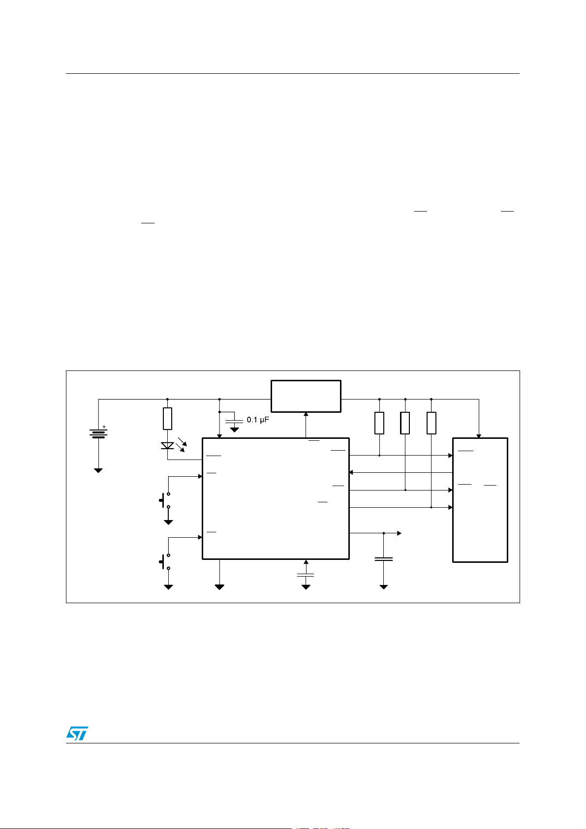
Figure 1. Application hookup
$#$#CONVERTER
$#$#CONVERTER
POWER-/3&%4
POWER-/3&%4
REGULATORETC
REGULATORETC
2
2
#
#
2
2
2%&
2%&
2
2
6
,%$
,%$
1. A resistor is required for open drain output type only. A 10 kΩ pull-up is sufficient in most applications.
2. Capacitor C
3. For the STM6601 the processor has to confirm the proper power-on during the fixed time period, t
feature prevents the user from turning on the system when there is a faulty power switch or an unresponsive
microprocessor.
is mandatory on V
REF
6
##
##
6##
6##
,/
,/
0"
0"
32
32
'.$
'.$
output (even if V
REF
34-
34-
34-
34-
%.%.
%.%.
#
#
is not used). Capacitor value of 1 µF is recommended.
REF
03
03
32$
32$
(/,$
(/,$
0"
0"
6
6
#
#
32$
32$
234
234
).4
).4
/54
/54
2%&
2%&
2
2
ON_BLANK
6
6
$$
$$
234
234
)/
)/
.-)OR).4
.-)OR).4
)/
)/
-#5
-#5
#05
#05
"!3%"!.$
"!3%"!.$
!-V
!-V
. This failsafe
Doc ID 15453 Rev 11 5/52
Description STM6600, STM6601
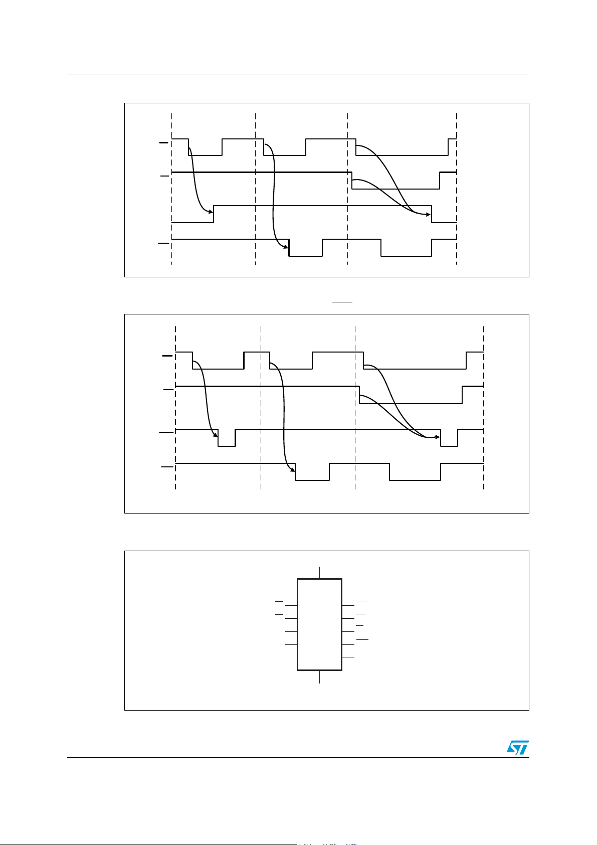
Figure 2. Basic functionality (option with enable deassertion after long push)
POWER-UP
(1)
INTERRUPT
(short push)
POWER-DOWN
(long push)
PB
SR
EN
INT interrupt interrupt
1. For power-up the battery voltage has to be above V
threshold.
TH+
Figure 3. Basic functionality (option with RST assertion after long push)
PB
SR
POWER-UP
(1)
INTERRUPT
(short push)
POWER-DOWN
(long push)
AM00243v1
RST
INT interrupt interrupt
1. For power-up the battery voltage has to be above V
Figure 4. Logic diagram
V
PB
SR
PS
HOLD
C
SRD
STM6600
STM6601
GND
TH+
CC
threshold.
EN (EN)
RST
INT
PB
VCC
V
REF
AM00243bv1
OUT
LO
AM00236v1
6/52 Doc ID 15453 Rev 11
STM6600, STM6601 Description
Table 2. Pin descriptions
Pin number Symbol Function
1V
CC
2SR
3V
4PS
5C
REF
HOLD
SRD
6PB
7VCC
8PB
LO
OUT
9EN or EN
10 RST
11 INT
Power supply input
Smart Reset™ button input
Precise 1.5 V voltage reference
PS
HOLD
input
Adjustable Smart Reset™ delay time input
Push-button input
Output for high threshold comparator output (V
Status of PB push-button input
Enable output
Reset output
Interrupt output
12 GND Ground
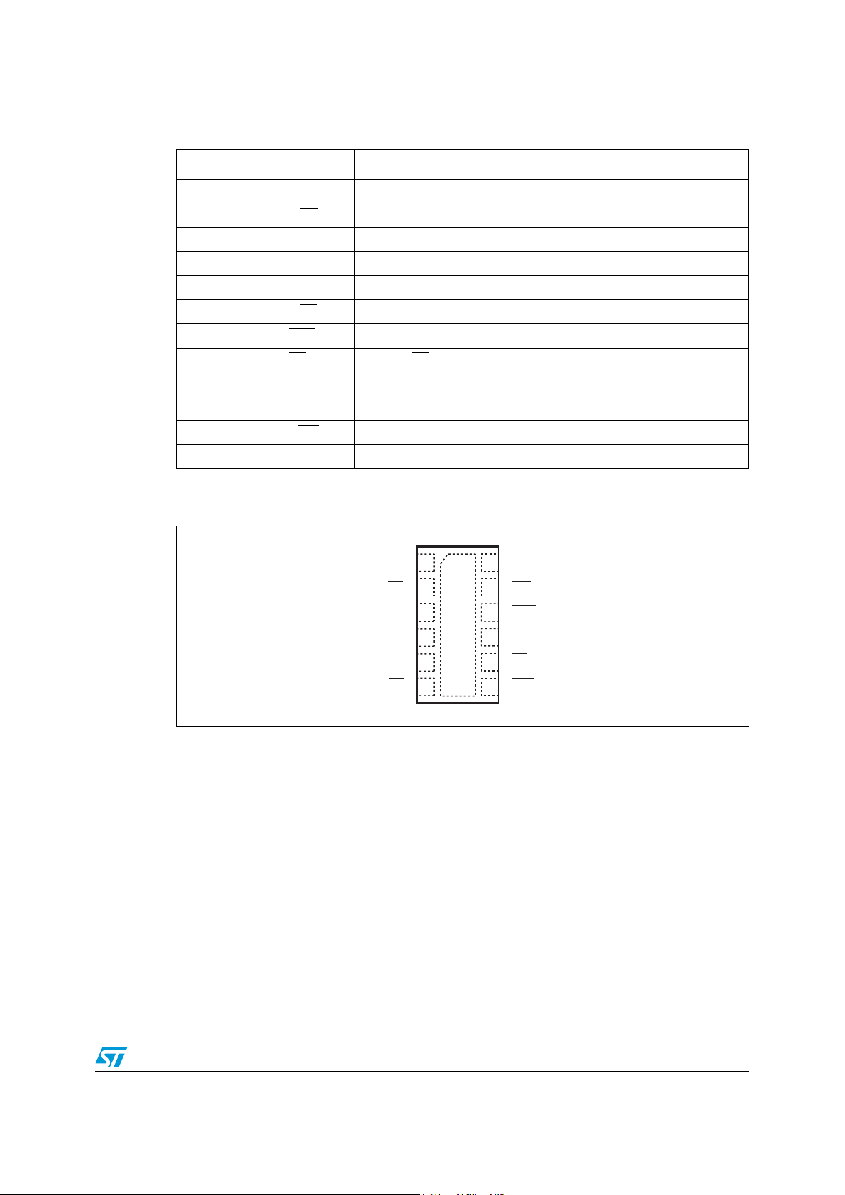
Figure 5. TDFN12 pin connections
V
CC
SR
V
REF
PS
HOLD
C
SRD
PB
1
2
3
4
5
67
12
11
10
9
8
GND
INT
RST
EN (EN)
PB
OUT
VCC
LO
TH+
)
AM00245v1
Doc ID 15453 Rev 11 7/52
Description STM6600, STM6601
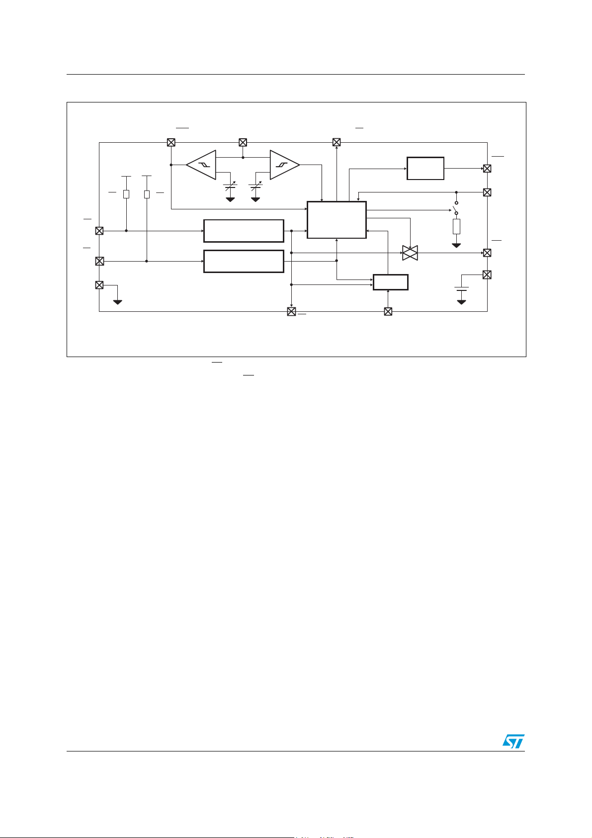
Figure 6. Block diagram
VCC
LO
+
V
V
CC
CC
(1)
R
PB
(2)
R
SR
V
–
TH+
V
CC
+
–
V
TH–
EN (EN)
Smart
PB
SR
GND
Glitch immunity
Edge detector debounce
Glitch immunity
Edge detector debounce
PB
logic
OUT
1. Internal pull-up resistor connected to PB input (see Table 5 for precise specifications).
2. Optional internal pull-up resistor connected to SR
device options).
3. Internal pull-down resistor is connected to PS
input (see Table 5 for precise specifications and Table 10 for detailed
input only during startup (see Figure 7, 8, 9, 10, 11, 12, 13, and 18).
HOLD
SRD logic
C
SRD
t
REC
generator
R
PSHOLD
RST
PS
HOLD
(3)
INT
V
REF
1.5 V
AM00237v3
8/52 Doc ID 15453 Rev 11

STM6600, STM6601 Pin descriptions
2 Pin descriptions
VCC - power supply input
is monitored during startup and normal operation for sufficient voltage level. Decouple
V
CC
the V
SR
This input is equipped with voltage detector with a factory-trimmed threshold and has ±8 kV
HBM ESD protection.
pin from ground by placing a 0.1 µF capacitor as close to the device as possible.
CC
- Smart Reset™ button input
Both PB
and SR buttons have to be pressed and held for t
period so the long push is
SRD
recognized and the reset is asserted (or the enable output is deasserted depending on the
option) - see Figure 15, 16, and 17.
Active low SR
input is usually connected to GND through the momentary push-button (see
Figure 1) and it has an optional 100 kΩ pull-up resistor. It is also possible to drive this input
using an external device with either open drain (recommended) or push-pull output. Open
drain output can be connected in parallel with push-button or other open drain outputs,
which is not possible with push-pull output. S
R input is monitored for falling edge after
power-up and must not be grounded permanently.
- external precise 1.5 V voltage reference
V
REF
This 1.5 V voltage reference is specified with very tight accuracy of 1% (see Table 5). It has
proper output voltage as soon as the reset output is deasserted (i.e. after t
expires) and
REC
it is disabled when the device enters standby mode. A mandatory capacitor needs to be
connected to V
output (even if V
REF
is not used). Capacitor value of 1 µF is
REF
recommended.
HOLD
input
PS
This input is equipped with a voltage detector with a factory-trimmed threshold. It is used to
confirm correct power-up of the device (if EN or EN
(if EN or EN
Forcing PS
is asserted).
high during power-up confirms the proper start of the application and keeps
HOLD
is not asserted) or to initiate a shutdown
enable output asserted. Because most processors have outputs in high-Z state before
initialization, an internal pull-down resistor is connected to PS
input during startup (see
HOLD
Figure 7, 8, 9, 10, 11, 12, 13, and 18).
Forcing the PS
signal low during normal operation deasserts the enable output (see
HOLD
Figure 14). Input voltage on this pin is compared to an accurate voltage reference.
- Smart Reset™ delay time input
C
SRD
A capacitor to ground determines the additional time (t
pressed and held before a long push is recognized. The connected C
charged with I
the C
capacitor reaches the V
SRD
current. Additional Smart Reset™ delay time t
SRD
voltage threshold. It is recommended to use a low
SRD
ESR capacitor (e.g. ceramic). If the capacitor is not used, leave the C
capacitor is connected, there is no t
and a long push is recognized right after t
SRD
) that PB with SR must be
SRD
SRD
capacitor is
SRD
ends when voltage on
pin open. If no
SRD
expires (see Figure 18 and 19).
Doc ID 15453 Rev 11 9/52
INT_Min

Pin descriptions STM6600, STM6601
PB - power ON switch
This input is equipped with a voltage detector with a factory-trimmed threshold and has
± 8 kV HBM ESD protection.
When the PB
asserted if the battery voltage is above the threshold V
button is pressed and held, the battery voltage is detected and EN (or EN) is
during the whole t
TH+
DEBOUNCE
period (see Figure 13).
A short push of the push-button during normal operation can initiate an interrupt through
debounced INT
either assert reset output RST
output (see Figure 14) and a long push of PB and SR simultaneously can
(see Figure 18) or deassert the EN or EN output (see
Figure 19) based on the option used.
Note: A switch to GND must be connected to this input (e.g. mechanical push-button, open drain
output of external circuitry, etc.), see Figure 1. This ensures a proper startup signal on PB
(i.e. a transition from full V
below specified VIL). PB input has an internal 100 kΩ pull-up
CC
resistor connected.
VCC
During power-up, VCC
successful power-up (i.e. during normal operation) VCC
- high threshold detection output
LO
is low when VCC supply voltage is below the V
LO
threshold. After
is low anytime undervoltage is
LO
TH+
detected (see Figure 13).
Output type is active low and open drain by default. Open drain output type requires a pullup resistor. A 10 kΩ is sufficient in most applications.
VCC
PB
If the push-button PB
If PB
t
deasserted (see Figure 22). PB
At startup on the STM6601 PB
assertion will be ignored until t
is floating when STM660x is in standby mode.
LO
- PB input state
OUT
is pressed, the pin stays low during the t
is asserted for the entire t
. If PB is asserted after t
INT_Min
DEBOUNCE
INT_Min
OUT
OUT
ON_BLANK
expire s, PB
ignores PB assertion during an undervoltage condition.
will respond only to the first PB assertion and any other
time period.
period, PB
OUT
DEBOUNCE
will then stay low for at least
OUT
will return high as soon as PB is
expires. This output is active low and open drain by
default. Open drain output type requires a pull-up resistor. A 10 kΩ is sufficient in most
applications.
10/52 Doc ID 15453 Rev 11

STM6600, STM6601 Pin descriptions
EN or EN - enable output
This output is intended to enable system power (see Figure 1). EN is asserted high after
a valid turn-on event has been detected and confirmed (i.e. push-button has been pressed
and held for t
DEBOUNCE
or more and V
CC
> V
voltage level has been detected - see
TH+
Figure 13). EN is released low if any of the conditions below occur:
a) the push-button is released before PS
Figure 9) or t
ON_BLANK
expires before PS
is driven high (valid for STM6600, see
HOLD
is driven high during startup (valid
HOLD
for both STM6600 and STM6601, see Figure 10 and 12).
b) PS
c) an undervoltage condition is detected for more than t
is driven low during normal operation (see Figure 14).
HOLD
SRD
+ t
INT_Min
+ t
DEBOUNCE
(see Figure 21).
d) a long push of the buttons is detected (only for the device with option “EN
deasserted by long push” - see Figure 19) or PS
t
ON_BLANK
after a long push of the buttons (only for the device with option “RST
is not driven high during
HOLD
asserted by long push” - see Figure 18).
Described logic levels are inverted in case of EN
- reset output
RST
This output pulls low for t
a) during startup. PB
for at least t
DEBOUNCE
:
REC
has been pressed (falling edge on the PB detected) and held
and VCC > V
output. Output type is push-pull by default.
(see Figure 7, 8, 9, 10, 11, 12 and 13 for
TH+
more details).
b) after long push detection (valid only for the device with option “RST
long push”). PB
more than t
by the external capacitor C
has been pressed (falling edge on the PB detected) and held for
DEBOUNCE
+ t
(additional Smart Reset™ delay time can be adjusted
SRD
) - see Figure 18.
SRD
asserted by
Output type is active low and open drain by default. Open drain output type requires a pullup resistor. A 10 kΩ is sufficient in most applications.
- interrupt output
INT
While the system is under normal operation (PS
asserted), the INT
a) V
CC
is driven low if:
falls below V
threshold (i.e. undervoltage is detected - see Figure 20 and
TH-
is driven high, power for application is
HOLD
21).
b) the falling edge on the PB
more. INT
INT
The state of the PB
either the assertion of the PB
on V
INT
.
CC
output is asserted low for at least t
is driven low after t
signal is held high during power-up.
output can be used to determine if the interrupt was caused by
OUT
input, or was due to the detection of an undervoltage condition
is detected and the push-button is held for t
DEBOUNCE
INT_Min
and stays low as long as PB is held. The
.
DEBOUNCE
or
Output type is active low and open drain by default. Open drain output type requires a pullup resistor. A 10 kΩ is sufficient in most applications.
GND - ground
Doc ID 15453 Rev 11 11/52

Operation STM6600, STM6601
3 Operation
The STM6600-STM6601 simplified smart push-button on/off controller with Smart Reset™
and power-on lockout enables and disables power for the application depending on pushbutton states, signals from the processor, and battery voltage.
Power-on
Because most of the processors have outputs in high-Z state before initialization, an internal
pull-down resistor is connected to PS
12, 13, and 18).
To power up the device the push-button PB
V
has to be above V
CC
below V
V
TH+
during the t
TH+
(see Figure 13). After t
goes low), reset output RST
for the whole t
TH+
DEBOUNCE
DEBOUNCE
is asserted for t
, the counter is reset and starts to count again when V
by the processor. During initialization, the processor sets the PS
On the STM6600 the PS
t
ON_BLANK
expiration, otherwise the enable signal is deasserted (EN goes low, EN goes
signal has to be set high prior to push-button release and
HOLD
high) - see Figure 7, 8, 9, and 10. The time up to push-button release represents the
maximum time allowed for the system to power up and initialize the circuits driving the
PS
input. If the PS
HOLD
signal is low at push-button release, the enable output is
HOLD
deasserted immediately, thus turning off the system power. If t
push-button release, the PS
state is checked at its expiration. This safety feature
HOLD
disables the power and prevents discharging the battery if the push-button is stuck or it is
held for an unreasonable period of time and the application is not responding (see Figure 8
and 10). PB
status, INT status and VCC undervoltage detection are not monitored until
power-up is completed.
input during startup (see Figure 7, 8, 9, 10, 11,
HOLD
has to be pressed for at least t
DEBOUNCE
period. If the battery voltage drops
DEBOUNCE
the enable signal is asserted (EN goes high, EN
and then the startup routine is performed
REC
ON_BLANK
signal high.
HOLD
expires prior to
and
CC
>
On the STM6601 the PS
signal has to be set high before t
HOLD
ON_BLANK
the enable signal is deasserted - see Figure 11 and 12. In this case the t
expires, otherwise
ON_BLANK
period is
the maximum time allowed for the power switch and processor to perform the proper poweron. If the PS
released immediately, thus turning off the system power. PB
undervoltage detection are not monitored during the entire t
signal is low at the end of the blanking period, the enable output is
HOLD
status, INT status and VCC
ON_BLANK
period. This failsafe
feature prevents the user from turning on the system when there is a faulty power switch or
an unresponsive microprocessor.
Push-button interrupt
If the device works under normal operation (i.e. PS
pressed for more than t
generated on the INT
NMI
) a safeguard routine can be performed and the power can be shut down by setting
PS
low - see Figure 14.
HOLD
DEBOUNCE
output. By connecting INT to the processor interrupt input (INT or
, a negative pulse with minimum t
is high) and the push-button PB is
HOLD
INT_Min
width is
Forced power-down mode
The PS
output can be forced low anytime during normal operation by the processor
HOLD
and can deassert the enable signal - see Figure 14.
Undervoltage detection
voltage drops below V
If V
CC
voltage threshold during normal operation, the INT output is
TH-
driven low (see Figure 20 and Figure 21).
12/52 Doc ID 15453 Rev 11

STM6600, STM6601 Operation
If an undervoltage condition is detected for t
DEBOUNCE
+ t
INT_Min
+ t
, the enable output is
SRD
deasserted (see Figure 21).
Hardware reset or power-down while system not responding
If the system is not responding and the system hangs, the PB
pressed simultaneously longer than t
a) either the reset output RST
only for the device with option “RST
b) or the power is disabled by EN or EN
DEBOUNCE
is asserted for t
+ t
INT_Min
REC
asserted by long push”) – see Figure 18
signal (valid only for the device with option
and SR push-buttons can be
+ t
, and then
SRD
and the processor is reset (valid
“EN deasserted by long push”) – see Figure 19
The t
is set by the external capacitor connected to the C
SRD
pin. SR input is monitored
SRD
for falling edge after power-up and must not be grounded permanently.
Standby
If the enable output is deasserted (i.e. EN is low or EN
standby mode with low current consumption (see Ta bl e 5). In standby mode PB
is high), the STM660x device enters
input is only
monitored for the falling edge. The external 1.5 V voltage reference is also disabled in
standby mode.
Doc ID 15453 Rev 11 13/52
Waveforms STM6600, STM6601
4 Waveforms
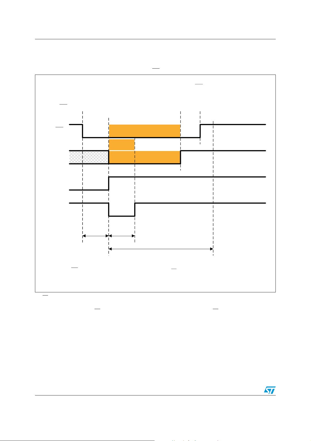
Figure 7. Successful power-up on STM6600 (PB released prior to t
PB released prior to t
expiration
Push-button pressed and
PB connected to GND
(1)
PB
sets PS
undervoltage detection
V
CC
ignored
HOLD
PS
processor
HOLD
PS
EN remains asserted
ignored
PS
HOLD
EN
(2)
(3)
internal pull-down resistor
connected to PS
HOLD
input
RST
ON_BLANK
HOLD
expiration)
state detected as high
ON_BLANK
t
DEBOUNCE
Note:
INT signal is held high during power-up (i.e. until PB release in this case).
V
is considered VCC > V
CC
1. PB detection on falling and rising edges.
2. Internal pull-down resistor 300 kΩ is connected to PS
3. EN signal is high even after PB
release, because processor sets PS
t
REC
TH+
.
t
ON_BLANK
input during power-up.
HOLD
HOLD
AM00247v3
signal high before PB is released.
14/52 Doc ID 15453 Rev 11
STM6600, STM6601 Waveforms
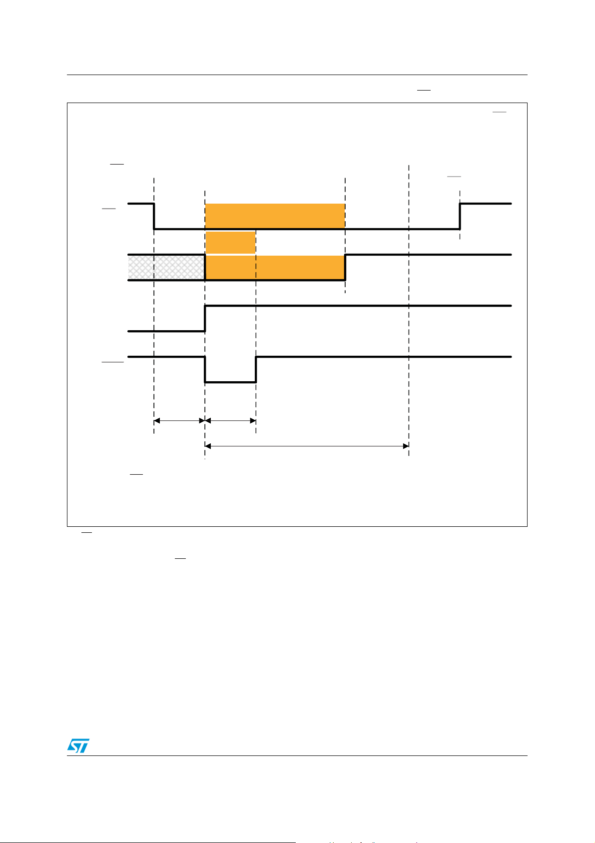
Figure 8. Successful power-up on STM6600 (t
Push-button pressed and
PB connected to GND
undervoltage detection
PB
(1)
V
PS
CC
HOLD
ignored
ignored
PS
HOLD
EN
(2)
(3)
internal pull-down resistor
connected to PS
RST
ON_BLANK
processor
sets PS
input
HOLD
expires prior to PB release)
t
ON_BLANK
expired prior to PB
release
PS
state detected as high
HOLD
EN remains asserted
HOLD
PB released
t
DEBOUNCE
Note:
INT signal is held high during power-up (i.e. until t
V
is considered VCC > V
CC
1. PB detection on falling and rising edges.
2. Internal pull-down resistor 300 kΩ is connected to PS
3. t
ON_BLANK
expires prior to PB release so PS
t
REC
.
TH+
is checked at its expiration.
HOLD
t
ON_BLANK
input during power-up.
HOLD
ON_BLANK
expires in this case).
AM00247bv2
Doc ID 15453 Rev 11 15/52
Waveforms STM6600, STM6601
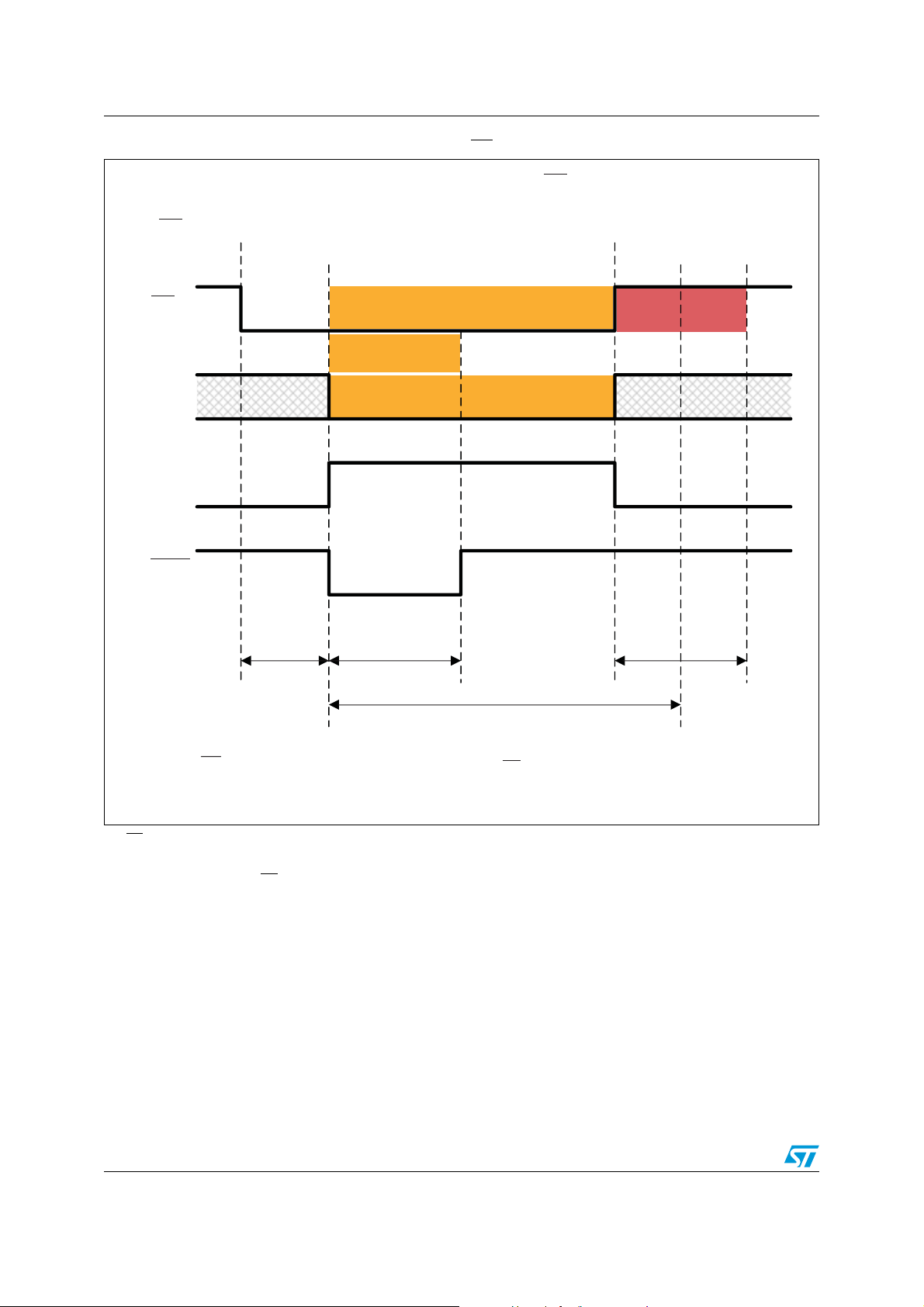
Figure 9. Unsuccessful power-up on STM6600 (PB released prior to t
PB released
Push-button pressed and
PB connected to GND
(1)
PB
undervoltage detection
V
CC
ignored
HOLD
PS
PS
EN deasserted
state detected as low
HOLD
ignored
PS
HOLD
EN
(2)
(3)
internal pull-down resistor
connected to PS
HOLD
input
RST
ON_BLANK
PB status
ignored
)
t
DEBOUNCE
Note:
INT signal is held high during power-up (i.e. until PB release in this case).
V
is considered VCC > V
CC
1. PB detection on falling and rising edges.
2. Internal pull-down resistor 300 kΩ is connected to PS
3. EN signal goes low with PB
release, because processor did not force PS
TH+
t
REC
.
t
ON_BLANK
input during power-up.
HOLD
signal high.
HOLD
t
EN_OFF
AM00248v3
16/52 Doc ID 15453 Rev 11

STM6600, STM6601 Waveforms
Figure 10. Unsuccessful power-up on STM6600 (t
t
ON_BLANK
PS
Push-button pressed and
PB connected to GND
PB
(1)
undervoltage detection ignored
V
CC
HOLD
PS
ignored
PS
HOLD
EN
(2)
(3)
internal pull-down resistor connected to
PS
HOLD
RST
ON_BLANK
expires prior to PB release)
expired prior to PB release
state detected as low
HOLD
EN is deasserted
input
PB released
PB status
ignored
t
DEBOUNCE
Note:
INT signal is held high during power-up (i.e. until t
V
is considered VCC > V
CC
1. PB detection on falling and rising edges.
2. Internal pull-down resistor 300 kΩ is connected to PS
3. t
ON_BLANK
expires prior to PB release so PS
t
REC
.
TH+
is checked at its expiration.
HOLD
t
ON_BLANK
input during power-up.
HOLD
ON_BLANK
t
EN_OFF
expires in this case).
AM00248bv2
Doc ID 15453 Rev 11 17/52

Waveforms STM6600, STM6601
Figure 11. Successful power-up on STM6601
Push-button pressed and
PB connected to GND
(1)
PB
(2)
PS
HOLD
(3)
EN
RST
t
DEBOUNCE
processor
sets PS
PB status and VCC undervoltage
HOLD
ignored
ignored
detection
PS
internal pull-down resistor
connected to PS
t
REC
t
ON_BLANK
HOLD
input
t
ON_BLANK
PS
HOLD
EN remains asserted
HOLD
expires
state detected as high
Note:
INT signal is held high during power-up (i.e. until t
V
is considered VCC > V
CC
1. PB detection on falling edge.
2. Internal pull-down resistor 300 kΩ is connected to PS
3. PS
signal is ignored during t
HOLD
EN signal remains asserted.
ON_BLANK
.
TH+
. When t
input during power-up.
HOLD
ON_BLANK
expires, the level of the PS
ON_BLANK
expires in the case of the STM6601).
AM00250v2
signal is high therefore the
HOLD
18/52 Doc ID 15453 Rev 11

STM6600, STM6601 Waveforms
Figure 12. Unsuccessful power-up on STM6601
Push-button pressed and
PB connected to GND
(1)
PB
HOLD
EN
(2)
(3)
PS
RST
t
DEBOUNCE
Note:
INT signal is held high during power-up (i.e. until t
V
is considered VCC > V
CC
PS
HOLD
intenal pull-down resistor
connected to PS
t
REC
TH+
t
ON_BLANK
PS
HOLD
EN deasserted
ignored
input
HOLD
.
expires
state detected as low
ON_BLANK
expires in the case of the STM6601).
Push-button pressed and
PB connected to GND
AM00238v2
1. PB detection on falling edge.
2. Internal pull-down resistor 300 kΩ is connected to PS
3. PS
signal is ignored during t
HOLD
the
EN signal goes low. Even releasing the PB button after the t
ON_BLANK
. When t
Doc ID 15453 Rev 11 19/52
input during power-up.
HOLD
ON_BLANK
expires, the level of the PS
ON_BLANK
signal is not high therefore
will not prevent this.
HOLD

Waveforms STM6600, STM6601
Figure 13. Power-up on STM660x with voltage dropout
Push-button pressed and
PB connected to GND
V
TH+
V
CC
VCC
LO
(1)
PB
HOLD
INT
(2)
(3)
PS
VCC goes above V
t
DEBOUNCE
V
CC
is counted again
drop
and
TH+
V
CC
under-
voltage
detected
internal pull-down resistor
connected to PS
HOLD
input
INT signal is held high during power-up
V
TH–
V
CC–Min
EN
RST
< t
DEBOUNCE
1. PB detection on falling and rising edges.
2. Internal pull-down resistor 300 kΩ is connected to PS
signal is held high during power-up.
3. INT
t
DEBOUNCE
t
REC
< t
ON_BLANK
input during power-up.
HOLD
AM00249v2
20/52 Doc ID 15453 Rev 11

STM6600, STM6601 Waveforms
Figure 14. PB interrupt
processor interrupt starts power-down sequence
PB
PS
HOLD
Note: V
Push-button pressed and
PB connected to GND
(1)
t
DEBOUNCE
is considered VCC > V
CC
PB status
ignored
VCC undervoltage
detection ignored
t
INT_Min
.
TH+
processor sets PS
and EN is deasserted
accordingly
PB status
ignored
t
EN_OFF
HOLD
low
AM00251v2
1. PB detection on falling edge.
Doc ID 15453 Rev 11 21/52

Waveforms STM6600, STM6601
Figure 15. Long push, PB pressed first
t
Push-button
PB is pressed
Push-button
SR is pressed
starts to
SRD
be counted
t
PB
SR
INT
DEBOUNCE
t
PB status
ignored
t
INT_Min
Figure 16. Long push, SR pressed first
Push-button
SR is pressed
Push-button
PB is pressed
DEBOUNCE
t
starts to
SRD
be counted
t
SRD
set by C
SRD
AM00257v1
PB
SR
INT
t
DEBOUNCE
PB status
ignored
t
INT_Min
t
SRD
set by C
SRD
AM00258v1
22/52 Doc ID 15453 Rev 11

STM6600, STM6601 Waveforms
Figure 17. Invalid long push
Push-button
PB is pressed
Any rising edge will stop
t
to count regardless
SRD
of glitch immunity
PB
SR
Push-button
SR is pressed
t
DEBOUNCE
t
starts to
SRD
be counted
< t
SRD
set by C
SRD
INT
PB status
ignored
t
INT_Min
AM00259v1
Doc ID 15453 Rev 11 23/52

Waveforms STM6600, STM6601
Figure 18. Long push (option with RST assertion)
expires
Push-button pressed
and PB connected to
GND
Push-button held even
SRD
expires
after t
therefore RST is asserted
t
BLANK
ON_
state detected as high
PS
HOLD
therefore EN remains high
After t
ON_BLANK
PB is monitored
for falling edge
t
PB
SRD
set by C
SR
INT can go high, if PB goes high,
but system freezes and processor
ignored
if system freezes, processor won’t
respond to any INT status change
t
INT_Min
won’t respond
PS
INT
HOLD
RST
(3, 4)
(2)
t
DEBOUNCE
PB status
undervoltage detection status ignored
V
CC
Note: EN is high.
1. t
period is set by external capacitor C
SRD
ignored during t
2. PB
3. PS
signal is ignored during t
HOLD
remains asserted, otherwise EN goes low.
INT_Min
.
ON_BLANK
4. Internal pull-down resistor 300 kΩ is connected to PS
.
SRD
. Its level is checked after t
(1)
SRD
(valid for STM6600 and STM6601)
internal pull-down resistor
input during startup when device is reset.
HOLD
t
ON_BLANK
PS
ignored
HOLD
connected to PS
t
REC
ON_BLANK
expires and if it is high the EN signal
HOLD
input
t
DEBOUNCE
AM00252v2
24/52 Doc ID 15453 Rev 11

STM6600, STM6601 Waveforms
Figure 19. Long push (option with enable deassertion)
Push-button
pressed and PB
connected to GND
PB
SR
(2)
INT
(3)
EN
PS
HOLD
t
DEBOUNCE
1. t
period is set by external capacitor C
SRD
ignored during t
2. PB
3. After t
expires EN is forced low.
SRD
INT_Min
PB status
ignored
undervoltage detection status ignored
V
CC
if system freezes, processor won’t
respond to any INT status change
INT can go high, if PB goes high,
but system freezes and processor
t
INT_Min
.
SRD
.
Push-button held even
after t
expires and
SRD
EN is deasserted
(1)
t
SRD
set by C
SRD
won’t respond
PB status
ignored
t
EN_OFF
EN_OFF
expires
After t
PB is monitored for
falling edge
t
DEBOUNCE
AM00253v2
Doc ID 15453 Rev 11 25/52

Waveforms STM6600, STM6601
Figure 20. Undervoltage detected for <t
V
undervoltage
CC
detected
V
CC
VCC
PS
(1)
LO
HOLD
INT
V
CC-Min
V
TH+
V
–
TH
V
CC
under-
voltage
detection
ignored
PB status ignored
EN
SRD
t
INT_Min
.
t
DEBOUNCE
1. V
goes above V
CC
period is set by external capacitor C
2. t
SRD
TH+
within t
thus power is not disabled after t
SRD
Figure 21. Undervoltage detected for >t
V
CC
undervoltage
detected
SRD
processor interrupt starts power-down sequence
processor sets PS
and EN is deasserted
accordingly
SRD
SRD
t
SRD
set by C
(2)
SRD
SRD
VCC is below V
thus power is disabled (EN goes low) and
expires.
PB status
ignored
t
EN_OFF
TH+
even after t
PB is monitored for regular startup
HOLD
expires
low
AM00254v1
(1)
V
VCC
PS
CC
LO
HOLD
V
CC-Min
INT
EN
t
DEBOUNCE
1. After t
2. t
SRD
expires VCC is still insufficient (below V
SRD
period is set by external capacitor C
V
TH+
V
–
TH
V
CC
under-
t
SRD
set by C
(2)
SRD
voltage
detection
ignored
PB status ignored
PB status
ignored
SRD
t
INT_Min
) thus power is disabled (EN goes low or EN goes high).
TH+
.
t
EN_OFF
AM00255v1
26/52 Doc ID 15453 Rev 11

STM6600, STM6601 Waveforms
Figure 22. PB
output waveform
OUT
<glitch immunity
(1,2,3,4)
PB
PB
OUT
t
DEBOUNCE
1. Pulses on PB shorter than glitch immunity are ignored.
2. Pulses on PB
3. Minimum pulse width on PB
shorter than t
DEBOUNCE
OUT
4. If push-button is held longer than t
are not recognized by PB
is t
INT_Min
DEBOUNCE
.
+ t
INT_Min
t
INT_min
.
OUT
, PB
goes high when the push-button is released.
OUT
AM00256v1
Doc ID 15453 Rev 11 27/52

Typical operating characteristics STM6600, STM6601
5 Typical operating characteristics
Figure 23. Supply current vs. temperature, normal state
7.0
6.5
6.0
(µA)
5.5
CC
5.0
4.5
Supply current, I
4.0
3.5
3.0
-40 -20 0 20 40 60 80
VCC = 5.5 V
VCC = 3.6 V
VCC = 2.0 V
Temperature, T
(°C)
A
Figure 24. Supply current vs. temperature, standby state
2.0
1.5
(µA)
CC
1.0
Supply current , I
0.5
0.0
-40 -20 0 20 40 60 80
Temper ature, T
A
(°C)
AM04701v1
VCC = 5.5 V
VCC = 3.6 V
VCC = 2.0 V
AM04702v1
28/52 Doc ID 15453 Rev 11

STM6600, STM6601 Typical operating characteristics
Figure 25. Supply current vs. supply voltage, normal state
7
6
5
(µA)
CC
4
3
2
Supply curr ent, I
1
0
2.0 2.5 3.0 3.5 4.0 4.5 5 .0 5.5
TA = 85 °C
TA = 25 °C
TA = 0 °C
TA = –40 °C
Supply voltage , V
CC
(V)
Figure 26. Supply current vs. supply voltage, standby state
1.5
TA = 85 °C
TA = 25 °C
1.0
(µA)
CC
0.5
Supply current, I
0.0
2.0 2.5 3.0 3.54.04.55.05.5
TA = 0 °C
TA = –40 °C
Supply voltage , V
CC
(V)
AM04703v1
AM04704v1
Doc ID 15453 Rev 11 29/52

Typical operating characteristics STM6600, STM6601
Figure 27. Threshold vs. temperature, V
3.50
3.45
3.40
(V)
TH+
3.35
3.30
Threshold, V
3.25
3.20
-40 -20 0 20 40 60 80
Tem perature, TA (°C)
= 3.4 V (typ.)
TH+
Figure 28. Threshold hysteresis vs. temperature, V
230
= 200 mV (typ.)
HYST
AM04705v1
220
(mV)
210
HTYST
200
190
180
Threshold hysteresis, V
170
-40 -20 0 20 40 60 80
Tem perature , TA (°C)
AM04706v1
30/52 Doc ID 15453 Rev 11

STM6600, STM6601 Typical operating characteristics
Figure 29. Debounce period vs. supply voltage
45
40
(ms)
35
DEBOUNCE
30
25
20
Debounce per iod, t
15
Figure 30. C
200
190
180
(nA)
170
SRD
160
150
140
130
charging current, I
120
SRD
C
110
100
TA = 85 °C
TA = 25 °C
TA = 0 °C
TA = –40 °C
3.544.555.5
Supply voltage, V
charging current vs. temperature, VCC = 3.6 V
SRD
CC
(V)
AM04707v1
VCC = 5.5 V
VCC = 3.6 V
VCC = 2 V
-40 -20 0 20 40 60 80
Temperature, T
(°C)
A
AM04708v1
Doc ID 15453 Rev 11 31/52

Typical operating characteristics STM6600, STM6601
Figure 31. Output low voltage vs. output low current, TA = 25 °C
0.30
0.25
(V)
OL
0.20
VCC=1.6V
VCC=3.6V
VCC=5.5V
0.15
0.10
Output low voltage, V
0.05
0.00
0123 45
Output low current, IOL (mA)
Note: Characteristics valid for all the outputs (EN, EN
Figure 32. Output high voltage vs. output high current, T
0.8
VCC=1.6V
(V)
- V
0.6
OH
CC
0.4
VCC=3.6V
VCC=5.5V
, RST, INT, PB
and VCCLO).
OUT
= 25 °C
A
AM04709v1
0.2
Output high voltage, V
0
00.511.52
Output high current, I
Note: Characteristics valid for EN and EN
outputs.
32/52 Doc ID 15453 Rev 11
OH
(mA)
AM04710v1

STM6600, STM6601 Typical operating characteristics
Figure 33. Output voltage vs. supply voltage, I
1
0.8
(V)
0.6
OUT
0.4
Output voltage, V
0.2
0
0123 45
Supply voltage, V
Note: Characteristics valid for all the outputs (EN, EN
Figure 34. Input voltage vs. temperature
1.05
= 1 mA, TA = 25 °C
OUT
(V)
CC
, RST, INT, PB
and VCCLO).
OUT
AM04711v1
1.04
1.03
(V)
IN
1.02
1.01
Input voltage, V
1.00
0.99
-40 -20 0 20 40 60 8 0
Note: Characteristics valid for PB
, SR and PS
Tem per ature, T
inputs.
HOLD
A
(°C)
VCC = 3.6 V
V
= 5.5 V
CC
AM04712v1
Doc ID 15453 Rev 11 33/52

Typical operating characteristics STM6600, STM6601
Figure 35. Reference output voltage vs. temperature, VCC = 2.0 V
1.520
1.515
I
I
REF
REF
= 0 mA
= 15 µA
(V)
Reference output voltage, V
1.510
REF
1.505
1.500
1.495
1.490
1.485
1.480
-40 -20 0 20 40 60 80
Note: 1 µF capacitor is connected to the V
Figure 36. Reference output voltage vs. load current, V
1.6
1.5
(V)
REF
1.4
1.3
1.2
1.1
Reference output voltage, V
1
050100150200250300
Note: 1 µF capacitor is connected to the V
Temperature, T
pin.
REF
Load current, I
pin.
REF
REF
A
(°C)
(µA)
= 2.0 V, TA = 25 °C
CC
AM04713v1
AM04714v1
34/52 Doc ID 15453 Rev 11

STM6600, STM6601 Typical operating characteristics
Figure 37. Reference output voltage vs. supply voltage, TA = 25 °C
1.520
1.515
(V)
1.510
REF
1.505
1.500
1.495
1.490
Reference output voltage, V
1.485
1.480
22.533.5 4 4.5 5 5.5
Note: 1 µF capacitor is connected to the V
Figure 38. Reference startup, I
REF
Supply voltage, V
pin.
REF
CC
(V)
= 15 µF, TA = 25 °C
I
REF
I
REF
= 0 µA
= 15 µA
AM04715v1
Note: 1 µF capacitor is connected to the V
Doc ID 15453 Rev 11 35/52
REF
pin.

Typical operating characteristics STM6600, STM6601
Figure 39. Reference response to steps on supply voltage, I
= 15 µA, TA = 25 °C
REF
Note: 1 Supply voltage goes from 3.6 V to 5.5 V and back to 3.6 V, ramp 1 V / 100 ns.
2 1 µF capacitor is connected to the V
REF
pin.
36/52 Doc ID 15453 Rev 11

STM6600, STM6601 Typical operating characteristics
Figure 40. Reference response to steps in load current, VCC = 3.6 V, TA = 25 °C
Note: 1 Supply voltage goes from 0 µA to 15 µA and back to 0 µA, ramp 1 µA / 100 ns.
2 1 µF capacitor is connected to the V
REF
pin.
Doc ID 15453 Rev 11 37/52

Maximum ratings STM6600, STM6601
6 Maximum ratings
Stressing the device above the rating listed inTable 3 may cause permanent damage to the
device. These are stress ratings only and operation of the device at these or any other
conditions above those indicated in Table 4 of this specification is not implied. Exposure to
absolute maximum rating conditions for extended periods may affect device reliability.
Table 3. Absolute maximum ratings
Symbol Parameter Min. Max. Unit Remarks
V
Input supply voltage –0.3 +7.0 V
CC
Input voltages on PB
C
SRD
Output voltages on EN (EN
INT
, SR, PS
), RST and
HOLD
and
–0.3 VCC + 0.3 V
–0.3 VCC + 0.3 V
–2 +2 kV Human body model (all pins)
V
V
V
V
V
T
T
SLD
θ
1. Reflow at peak temperature of 260 °C. The time above 255 °C must not exceed 30 seconds.
Electrostatic protection
ESD
Electrostatic protection –1000 +1000 V Charged device model
ESD
Electrostatic protection –200 +200 V Machine model
ESD
Point discharge on PB and SR inputs –8 +8 kV IEC61000-4-2
ESD
Air discharge on PB and SR inputs –15 +15 kV IEC61000-4-2
ESD
T
Operating ambient temperature –40 +85 °C
A
Storage temperature –45 +150 °C
STG
(1)
Lead solder temperature for 10 seconds +260 °C
Thermal resistance (junction to ambient) +132.4 °C/W
JA
–8 +8 kV Human body model (PB
and SR)
38/52 Doc ID 15453 Rev 11

STM6600, STM6601 DC and AC characteristics
7 DC and AC characteristics
This section summarizes the operating measurement conditions and the DC and AC
characteristics of the device. The parameters inTab le 5 that follow are derived from tests
performed under the measurement conditions summarized in Table 4. Designers should
check that the operating conditions in their circuit match the operating conditions when
relying on the quoted parameters.
Table 4. Operating and AC measurement conditions
Parameter Condition Unit
V
supply voltage 1.6 to 5.5 V
CC
Ambient operating temperature (T
Input rise and fall times ≤
) –40 to 85 °C
A
_
5ns
Table 5. DC and AC characteristics
Symbol Parameter Test condition
V
I
Supply voltage 1.6 5.5 V
CC
V
= 3.6 V, no load 6.0 8.0 µA
CC
Supply current
CC
Standby mode, enable
deasserted, V
CC
Power-on lockout voltage
V
(see Ta bl e 1 0 for detailed
TH+
listing)
V
HYST
Threshold hysteresis (see
Ta ble 1 0 for detailed listing)
Forced power-off voltage
V
(see Ta bl e 1 0 for detailed
TH–
listing)
t
TH–
Undervoltage detection to
INT
delay
≥ 2.0 V203244ms
V
CC
(1)
= 3.6 V
Min. Typ.
(2)
Max. Unit
0.6 1.0 µA
2.40 2.50 2.60
3.00 3.10 3.20
3.20 3.30 3.40
3.29 3.40 3.51
3.39 3.50 3.61
200
500
V
– V
TH+
HYST
V
mV
V
t
ON_BLANK
Blanking period (see
Ta ble 1 0 for detailed
(3)
listing)
RST
assertion to EN (EN)
assertion delay during
power-up
1.4 2.2 3.0
11.2 17.6 24.0
V
= 3.6 V 100 ns
CC
Doc ID 15453 Rev 11 39/52
s5.6 8.8 12.0

DC and AC characteristics STM6600, STM6601
Table 5. DC and AC characteristics (continued)
Symbol Parameter Test condition
PB
(1)
Min. Typ.
(2)
Max. Unit
V
IL
V
IH
t
DEBOUNCE
R
PB
SR
V
IL
V
IH
t
DEBOUNCE
(4)
R
SR
PB
OUT
V
OL
VCC
LO
V
OL
Input low voltage VCC ≥ 2.0 V, enable asserted 0.99 V
Input high voltage VCC ≥ 2.0 V, enable asserted 1.05 V
Debounce period VCC ≥ 2.0 V203244ms
Internal pull-up resistor VCC = 5.5 V, input asserted 65 100 135 kΩ
Input low voltage 0.99 V
Input high voltage 1.05 V
Debounce period 20 32 44 ms
Internal pull-up resistor V
Output low voltage
leakage current
PB
OUT
Output low voltage
VCC
leakage current
LO
= 5.5 V, input asserted 65 100 135 kΩ
CC
V
CC
PB
V
PBOUT
drain
V
CC
VCC
V
VCCLO
drain
= 2 V, I
asserted
OUT
= 3 V, PB
= 2 V, I
asserted
LO
= 3 V, VCC
SINK
SINK
= 1 mA,
open
OUT
= 1 mA,
open
LO
–0.1 +0.1 µA
–0.1 +0.1 µA
0.3 V
0.3 V
PS
HOLD
V
V
Input low voltage VCC ≥ 2.0 V0.99V
IL
Input high voltage VCC ≥ 2.0 V1.05 V
IH
Glitch immunity 1 80 µs
PS
PS
leakage current V
HOLD
to enable
HOLD
PSHOLD
= 0.6 V –0.1 0.1 µA
propagation delay
Pull-down resistor
R
PSHOLD
connected internally during
V
PSHOLD
= 5.5 V 195 300 405 kΩ
power-up
40/52 Doc ID 15453 Rev 11
30 µs

STM6600, STM6601 DC and AC characteristics
Table 5. DC and AC characteristics (continued)
Symbol Parameter Test condition
C
SRD
I
V
t
SRD
SRD
SRD
C
charging current 100 150 200 nA
SRD
= 3.6 V, load on V
V
CC
C
voltage threshold
SRD
Additional Smart Reset™
delay time
100 kΩ and mandatory 1 µF
capacitor, T
External C
= 25 °C
A
connected 10 s/µF
SRD
EN, EN
V
V
OL
V
OH
t
EN_OFF
= 2 V, I
Output low voltage
(5)
Output high voltage
(6)
enable off to enable on VCC ≥ 2.0 V406488ms
EN, EN
leakage current VEN = 2 V, enable open drain –0.1 +0.1 µA
CC
enable asserted
V
= 2 V, I
CC
enable asserted
= 1 mA,
SINK
SOURCE
(1)
pin
REF
= 1 mA,
Min. Typ.
– 0.3 V
V
CC
(2)
Max. Unit
1.5 V
0.3 V
RST
V
t
REC
= 2 V, I
V
Output low voltage
OL
CC
RST
asserted
RST pulse width VCC ≥ 2.0 V 240 360 480 ms
RST
leakage current V
= 3V –0.1 +0.1 µA
RST
SINK
= 1 mA,
0.3 V
INT
= 2 V, I
V
CC
INT
asserted
= 3 V –0.1 +0.1 µA
INT
= 3.6 V, load on V
V
CC
100 kΩ and mandatory 1 µF
t
V
REF
V
OL
INT_Min
V
REF
Output low voltage
Minimum INT pulse width VCC ≥ 2.0 V203244ms
INT
leakage current V
1.5 V voltage reference
capacitor, T
1. Valid for ambient operating temperature: TA = –40 to 85 °C; VCC = 1.6 V to 5.5 V (except where noted).
2. Typical values are at T
3. This blanking time allows the processor to start up correctly (see Figure 7, 8, 9, 10, 11, 12).
4. The internal pull-up resistor connected to the SR
5. Valid for push-pull only.
6. Minimum delay time between enable deassertion and enable reassertion, allowing the application to complete the power-down
properly. PB
is ignored during this period.
= +25 °C.
A
input is optional (see Table 10 for detailed device options).
SINK
= 25 °C
A
= 1 mA,
REF
pin
1.485
–1%
1.5
0.3 V
1.515
+1%
V
Doc ID 15453 Rev 11 41/52

Package mechanical data STM6600, STM6601
8 Package mechanical data
In order to meet environmental requirements, ST offers these devices in different grades of
ECOPACK
specifications, grade definitions and product status are available at: www.st.com.
ECOPACK
®
packages, depending on their level of environmental compliance. ECOPACK®
®
is an ST trademark.
42/52 Doc ID 15453 Rev 11

STM6600, STM6601 Package mechanical data
Figure 41. TDFN12 (2 x 3 mm) package outline
INDEX AREA
(D/2xE/2)
0.10
C
A
0.08
C
D
2x
0.10 C
0.10 C
TOP VIEW
SIDE VIEW
e
b
1
6
A
B
E
A1
SEATING
PLANE
0.10 C A B
C
PIN#1 ID
INDEX AREA
(D/2xE/2)
L
12
BOTTOM VIEW
Table 6. TDFN12 (2 x 3 mm) package mechanical data
7
8070542_A
mm inches
Symbol
Min. Typ. Max. Min. Typ. Max.
A 0.70 0.75 0.80 0.028 0.030 0.031
A1 0.00 0.02 0.05 0.000 0.001 0.002
b 0.15 0.20 0.25 0.006 0.008 0.010
D 3.00 BSC 0.118
E 2.00 BSC 0.079
e 0.50 0.020
L 0.45 0.55 0.65 0.018 0.022 0.026
Doc ID 15453 Rev 11 43/52

Package mechanical data STM6600, STM6601
Figure 42. TDFN12 (2 x 3 mm) recommended footprint
X
X
X
X
X
X
Note: Drawing not to scale.
X
X
$IMENSIONS
MM
INCHES
!-
44/52 Doc ID 15453 Rev 11

STM6600, STM6601 Package mechanical data
Figure 43. Carrier tape for TDFN12 (2 x 3 mm) package
P
D
T
A
TOP COVER
TAPE
K
0
0
CENTER LINES
OF CAVITY
P
2
B
0
USER DIRECTION OF FEED
0
P
1
E
F
W
AM03073v1
Table 7. Carrier tape dimensions for TDFN12 (2 x 3 mm) package
Package W D E P
TDFN12
12.00
±0.30
1.50
+0.10/
–0.00
1.75
±0.10
4.00
±0.10
P
0
2.00
±0.10
FA0B
2
5.50
±0.05
2.30
±0.10
0
3.20
±0.10
K
0
1.10
±0.01
P
1
4.00
±0.10
TUnit
0.30
±0.05
Bulk
qty.
mm 3000
Doc ID 15453 Rev 11 45/52

Part numbering STM6600, STM6601
9 Part numbering
Table 8. STM6600 ordering information scheme
Example: STM660 0 F Q 2 4 DM 6 F
Device type
STM660
Startup process
0: PB
must be held low until the PS
Input and output types
(1)
confirmation
HOLD
A: active high EN output, long push asserts RST, pull-up on SR
B: active low EN output, long push asserts RST, pull-up on SR
C: active high EN output, long push deasserts EN, pull-up on SR
D: active low EN output, long push deasserts EN, pull-up on SR
E: active high EN output, long push asserts RST, no resistor on SR
F: active low EN output, long push asserts RST, no resistor on SR
G: active high EN output, long push deasserts EN, no resistor on SR
H: active low EN output, long push deasserts EN, no resistor on SR
V
threshold voltage
TH+
A: 2.50 V
Q: 3.30 V
S: 3.40 V
U: 3.50 V
V
voltage hysteresis
HYST
2: 200 mV
5: 500 mV
t
ON_BLANK
blanking period
2: 1.4 s (min.)
4: 5.6 s (min.)
5: 11.2 s (min.)
(1)
(1)
(1)
46/52 Doc ID 15453 Rev 11

STM6600, STM6601 Part numbering
Table 8. STM6600 ordering information scheme (continued)
Example: STM660 0 F Q 2 4 DM 6 F
Package
DM: TDFN12
Temperature range
6: –40 °C to +85 °C
Shipping method
F: ECOPACK
1. Other options are offered. Minimum order quantities may apply. Please contact local ST sales office for availability.
®
package, tape and reel
Doc ID 15453 Rev 11 47/52

Part numbering STM6600, STM6601
Table 9. STM6601 ordering information scheme
Example: STM660 1 G U 2 B DM 6 F
Device type
STM660
Startup process
1: PB
can be released before the PS
Input and output types
(1)
confirmation
HOLD
A: active high EN output, long push asserts RST, pull-up on SR
B: active low EN output, long push asserts RST, pull-up on SR
C: active high EN output, long push deasserts EN, pull-up on SR
D: active low EN output, long push deasserts EN, pull-up on SR
G: active high EN output, long push deasserts EN, no resistor on SR
V
threshold voltage
TH+
(1)
M: 3.10 V
Q: 3.30 V
S: 3.40 V
U: 3.50 V
voltage hysteresis
V
HYST
(1)
2: 200 mV
t
ON_BLANK
blanking period
(1)
B: 1.4 s (min.)
D: 5.6 s (min.)
Package
DM: TDFN12
Temperature range
6: –40 °C to +85 °C
Shipping method
®
F: ECOPACK
1. Other options are offered. Minimum order quantities may apply. Please contact local ST sales office for availability.
package, tape and reel
48/52 Doc ID 15453 Rev 11

STM6600, STM6601 Product selector
10 Product selector
Table 10. STM6600 product selector
t
ON_BLANK
(s)
at reset
(min.)
Top
marking
(3)
Full part number
EN or
(1)
EN
After
long
push
(2)
Internal
resistor
on SR
input
Power-on
lockout
voltage
V
TH+
(V)
Forced
power-off
voltage
V
(V)
TH-
t
ON_BLANK
(s)
at startup
(min.)
STM6600AS24DM6F EN RST pull-up 3.40 3.20 5.6 5.6
STM6600BQ24DM6F EN
RST pull-up 3.30 3.10 5.6 5.6
STM6600CS25DM6F EN EN pull-up 3.40 3.20 11.2 —
STM6600DA55DM6F EN
STM6600DQ25DM6F EN
STM6600DU25DM6F EN
STM6600ES24DM6F
STM6600FQ24DM6F
STM6600GS22DM6F
STM6600GS25DM6F
STM6600GU22DM6F
STM6600HA55DM6F
STM6600HQ25DM6F
STM6600HU25DM6F
(4)
(4)
(4)
(4)
(4)
(4)
(4)
(4)
EN pull-up 2.50 2.00 11.2 —
EN pull-up 3.30 3.10 11.2 —
EN pull-up 3.50 3.30 11.2 —
EN RST — 3.40 3.20 5.6 5.6
EN RST — 3.30 3.10 5.6 5.6
EN EN — 3.40 3.20 1.4 —
EN EN — 3.40 3.20 11.2 —
EN EN — 3.50 3.30 1.4 —
EN EN — 2.50 2.00 11.2 —
EN EN — 3.30 3.10 11.2 —
EN EN — 3.50 3.30 11.2 —
pyww
AS24
pyww
BQ24
pyww
CS25
pyww
DA55
pyww
DQ25
pyww
DU25
pyww
ES24
pyww
FQ24
pyww
GS22
pyww
GS25
pyww
GU22
pyww
HA55
pyww
HQ25
pyww
HU25
1. EN (or EN) output is push-pull. RST, INT, PB
2. After t
will be deasserted. The additional Smart Reset™ delay time, t
connecting the external capacitor to the C
3. Where “p” = assembly plant, “y” = assembly year (0 to 9) and “ww” = assembly work week (01 to 52).
4. Please contact local ST sales office for availability.
expires through long push, either device reset (RST) will be activated for t
SRD
SRD
and VCC
OUT
pin.
outputs are open drain.
LO
(240 ms min.) or the EN (or EN) pin
, can be adjusted by the user at 10 s/µF (typ.) by
SRD
REC
Doc ID 15453 Rev 11 49/52

Product selector STM6600, STM6601
Table 11. STM6601 product selector
t
ON_BLANK
(s)
at reset
(min.)
Top
marking
(3)
Full part number
EN or
(1)
EN
After
long
push
(2)
Internal
resistor
on SR
input
Power-on
lockout
voltage
V
TH+
(V)
Forced
power-off
voltag e
V
(V)
TH-
t
ON_BLANK
(s)
at startup
(min.)
STM6601AQ2BDM6F EN RST pull-up 3.30 3.10 1.4 1.4
STM6601AU2DDM6F EN RST
STM6601BM2DDM6F EN
STM6601BS2BDM6F EN
RST pull-up 3.10 2.90 5.6 5.6
RST pull-up 3.40 3.20 1.4 1.4
pull-up 3.50 3.30 5.6 5.6
STM6601CM2DDM6F EN EN pull-up 3.10 2.90 5.6 —
STM6601CQ2BDM6F EN EN pull-up 3.30 3.10 1.4 —
STM6601CU2BDM6F EN EN pull-up 3.50 3.30 1.4 —
STM6601DS2BDM6F EN
STM6601GU2BDM6F
1. EN (or EN) output is push-pull. RST, INT, PB
2. After t
will be deasserted. The additional Smart Reset
connecting the external capacitor to the C
3. Where “p” = assembly plant, “y” = assembly year (0 to 9) and “ww” = assembly work week (01 to 52).
4. Please contact local ST sales office for availability.
expires through long push, either device reset (RST) will be activated for t
SRD
(4)
EN pull-up 3.40 3.20 1.4 —
EN EN — 3.50 3.30 1.4 —
OUT
SRD
and VCC
™
delay time, t
pin.
outputs are open drain.
LO
(240 ms min.) or the EN (or EN) pin
, can be adjusted by the user at 10 s/µF (typ.) by
SRD
REC
pyww
AQ2B
pyww
AU2D
pyww
BM2D
pyww
BS2B
pyww
CM2D
pyww
CQ2B
pyww
CU2B
pyww
DS2B
pyww
GU2B
50/52 Doc ID 15453 Rev 11

STM6600, STM6601 Revision history
11 Revision history
Table 12. Document revision history
Date Revision Changes
04-Mar-2009 1 Initial release.
Updated text in Section 2, Section 3, Figure 11, 12; updated Figure 1, 7,
05-Jun-2009 2
23-Jul-2009 3 Updated text in Features, Table 1, 8, 9, and 10; reformatted document.
22-Oct-2009 4
25-Jan-2010 5 Updated Figure 6, Section 2, Tab le 5 ; textual update to “Smart Reset
9, 14, 18, 19, 43, Ta bl e 3 , 5, 8, 9, 10; added Figure 8, 10, Ta b le 7 ;
reformatted document.
Updated Section 2, Table 5, Ta b l e 1 0 , Figure 1, 7, 8, 9, 10, 11, 12, 14, 18,
title of Section 10; added Section 5: Typical operating characteristics
(Figure 23 through 40); document status upgraded to full datasheet.
™
”.
13-Apr-2010 6
07-Jun-2010 7
10-Sep-2010 8
24-Feb-2011 9 Updated Ta b l e 1 1 - removed footnote 4.
12-May-2011 10
26-Jun-2012 11
Updated Figure 1, 6, 7, 8, 9, 10, 11, 12, 13, Section 2, Section 3, Ta b l e 3 ,
5, 8, 9, 10.
Reformatted Figure 1 and Figure 42, corrected typo in Section 3, added
option A to Ta bl e 8 , updated Table 10 and separated Tab l e 1 0 to Tab le 1 0
and Ta bl e 1 1 .
Updated standby current to 0.6 µA throughout datasheet; removed
footnote 2 of Figure 14; updated Tab le 8 , 9, 11; minor textual updates.
Updated Ta bl e 8 , Ta bl e 1 0 and Tab le 11, minor text and typo
modifications throughout document.
Updated Section 1: Description, “SR
Section 2: Pin descriptions and “Hardware reset or power-down while
system not responding” in Section 3: Operation, added cross-references
in Section 6: Maximum ratings and Section 7: DC and AC characteristics.
- Smart Reset™ button input” in
Doc ID 15453 Rev 11 51/52

STM6600, STM6601
y
Please Read Carefully:
Informatio n in this document is provided solely in connection with ST products. STMicroelectronics NV and its subsidiaries (“ST”) reserve the
right to make changes, corrections, modifications or improvements, to this document, and the products and services described herein at an
time, without notice.
All ST products are sold pursuant to ST’s terms and conditions of sale.
Purchasers are solely responsible for the choice, selection and use of the ST products and services described herein, and ST assumes no
liability whatsoever relating to the choice, selection or use of the ST products and services described herein.
No license, express or imp lied, by estoppel or otherwise, to any intellectual property rights is granted under this do cument. If any part of this
document refers to any third party products or services it shall not be deemed a license grant by ST for the use of such third party products
or services, or any intellectual property contained therein or considered as a warranty covering the use in any manner whatsoever of such
third party products or services or any intellectual property contained therein.
UNLESS OTHERWISE SET FORTH IN ST’S TERMS AND CONDITIONS OF SALE ST DISCLAIMS ANY EXPRESS OR IMPLIED
WARRANTY WITH RESPECT TO THE USE AND/OR SALE OF ST PRODUCTS INCLUDING WITHOUT LIMITATION IMPLIED
WARRANTIES OF MERCHANTABILITY, FITNESS FOR A PARTICULAR PURPOSE (AND THEIR EQUIVALENTS UNDER THE LAWS
OF ANY JURISDICTION), OR INFRINGEMENT OF ANY PATENT, COPYRIGHT OR OTHER INTELLECTUAL PROPERTY RIGHT.
UNLESS EXPRESSLY APPROVED IN WRITING BY TWO AUTHORIZED ST REPRESENTATIVES, ST PRODUCTS ARE NOT
RECOMMENDED, AUTHORIZED OR WARRANTED FOR USE IN MILITARY, AIR CRAFT, SPACE, LIFE SAVING, OR LIFE SUSTAINING
APPLICATIONS, NOR IN PRODUCTS OR SYSTEMS WHERE FAILURE OR MALFUNCTION MAY RESULT IN PERSONAL INJURY,
DEATH, OR SEVERE PROPERTY OR ENVIRONMENTAL DAMAGE. ST PRODUCTS WHICH ARE NOT SPECIFIED AS "AUTOMOTIVE
GRADE" MAY ONLY BE USED IN AUTOMOTIVE APPLICATIONS AT USER’S OWN RISK.
Resale of ST products with provisions different from the statements and/or technical features set forth in this document shall immediately void
any warranty granted by ST for the ST product or service described herein and shall not create or extend in any manner whatsoever, any
liability of ST.
ST and the ST logo a re trademarks or registered trademarks of ST in various countries.
Information in this document supersedes and replaces all information previously supplied.
The ST logo is a registered trademark of STMicroelectronics. All other names are the property of their respective owners.
© 2012 STMicroelectronics - All rights reserved
STMicroelectronics group of companies
Australia - Belgium - Brazil - Canada - China - Czech Republic - Finland - France - Germany - Hong Kong - India - Israel - Italy - Japan -
Malaysia - Malta - Morocco - Philippines - Singapore - Spain - Sweden - Switzerland - United Kingdom - United States of America
www.st.com
52/52 Doc ID 15453 Rev 11
 Loading...