

Page 1
Smart Reset
™
with push-button controlled output delay
Features
■ Dual Smart Reset™ push-button inputs, with
user-selectable extended reset setup delay
(by two-state input logic): t
■ Push-button controlled reset pulse duration
(no fixed nor minimum pulse width guaranteed)
■ No power-on reset
■ Dual reset outputs
–RST1
- active-low, open-drain
– RST2 - active-high, push-pull
■ Fixed Smart Reset™ input logic voltage levels
■ Broad operating voltage range 1.65 V to 5.5 V,
inactive reset output levels valid down to 1.0 V
■ Low supply current 1.5 µA
■ Operating temperature: –30 °C to +85 °C
■ TDFN8 package: 2 mm x 2 mm x 0.75 mm
■ RoHS compliant
= 6, 10 s (min.)
SRC
STM6520
Dual push-button
TDFN8 (DG)
2 mm x 2 mm
Applications
■ Mobile phones, smartphones
■ e-books
■ MP3 players
■ Games
■ Portable navigation devices
■ Any application that requires delayed reset
push-button(s) response for improved system
stability
January 2011 Doc ID15953 Rev 6 1/23
www.st.com
1
Page 2

Contents STM6520
Contents
1 Description . . . . . . . . . . . . . . . . . . . . . . . . . . . . . . . . . . . . . . . . . . . . . . . . . 5
2 Device overview . . . . . . . . . . . . . . . . . . . . . . . . . . . . . . . . . . . . . . . . . . . . 6
3 Pin descriptions . . . . . . . . . . . . . . . . . . . . . . . . . . . . . . . . . . . . . . . . . . . . 7
3.1 Power supply (VCC) . . . . . . . . . . . . . . . . . . . . . . . . . . . . . . . . . . . . . . . . . . 7
3.2 Ground (V
3.3 Smart Reset™ inputs (SR0
3.4 User-selectable Smart Reset™ delay (DSR) . . . . . . . . . . . . . . . . . . . . . . . 7
3.5 Reset outputs (RST1
) . . . . . . . . . . . . . . . . . . . . . . . . . . . . . . . . . . . . . . . . . . . . . . . 7
SS
, SR1) . . . . . . . . . . . . . . . . . . . . . . . . . . . . . . . 7
, RST2) . . . . . . . . . . . . . . . . . . . . . . . . . . . . . . . . . . . 7
4 Typical application diagram . . . . . . . . . . . . . . . . . . . . . . . . . . . . . . . . . . . 8
5 Typical operating characteristics . . . . . . . . . . . . . . . . . . . . . . . . . . . . . 10
6 Maximum rating . . . . . . . . . . . . . . . . . . . . . . . . . . . . . . . . . . . . . . . . . . . . 11
7 DC and AC parameters . . . . . . . . . . . . . . . . . . . . . . . . . . . . . . . . . . . . . . 12
8 Package mechanical data . . . . . . . . . . . . . . . . . . . . . . . . . . . . . . . . . . . . 14
9 Package footprint . . . . . . . . . . . . . . . . . . . . . . . . . . . . . . . . . . . . . . . . . . 16
10 Tape and reel information . . . . . . . . . . . . . . . . . . . . . . . . . . . . . . . . . . . . 17
11 Ordering information . . . . . . . . . . . . . . . . . . . . . . . . . . . . . . . . . . . . . . . 20
12 Package marking information . . . . . . . . . . . . . . . . . . . . . . . . . . . . . . . . 21
13 Revision history . . . . . . . . . . . . . . . . . . . . . . . . . . . . . . . . . . . . . . . . . . . 22
2/23 Doc ID 15953 Rev 6
Page 3

STM6520 List of tables
List of tables
Table 1. Signal names . . . . . . . . . . . . . . . . . . . . . . . . . . . . . . . . . . . . . . . . . . . . . . . . . . . . . . . . . . . . 6
Table 2. Absolute maximum ratings . . . . . . . . . . . . . . . . . . . . . . . . . . . . . . . . . . . . . . . . . . . . . . . . . 11
Table 3. Operating and measurement conditions . . . . . . . . . . . . . . . . . . . . . . . . . . . . . . . . . . . . . . . 12
Table 4. DC and AC characteristics . . . . . . . . . . . . . . . . . . . . . . . . . . . . . . . . . . . . . . . . . . . . . . . . . 13
Table 5. TDFN – 8-lead 2 x 2 x 0.75 mm, 0.5 mm package mechanical data . . . . . . . . . . . . . . . . . 15
Table 6. Parameter for landing pattern - TDFN – 8-lead 2 x 2 mm package . . . . . . . . . . . . . . . . . . 16
Table 7. Carrier tape dimensions . . . . . . . . . . . . . . . . . . . . . . . . . . . . . . . . . . . . . . . . . . . . . . . . . . . 17
Table 8. Reel dimensions . . . . . . . . . . . . . . . . . . . . . . . . . . . . . . . . . . . . . . . . . . . . . . . . . . . . . . . . . 18
Table 9. Ordering information scheme . . . . . . . . . . . . . . . . . . . . . . . . . . . . . . . . . . . . . . . . . . . . . . . 20
Table 10. Package marking . . . . . . . . . . . . . . . . . . . . . . . . . . . . . . . . . . . . . . . . . . . . . . . . . . . . . . . . 21
Table 11. Document revision history . . . . . . . . . . . . . . . . . . . . . . . . . . . . . . . . . . . . . . . . . . . . . . . . . 22
Doc ID 15953 Rev 6 3/23
Page 4

List of figures STM6520
List of figures
Figure 1. Logic diagram . . . . . . . . . . . . . . . . . . . . . . . . . . . . . . . . . . . . . . . . . . . . . . . . . . . . . . . . . . . . 5
Figure 2. Pin connections . . . . . . . . . . . . . . . . . . . . . . . . . . . . . . . . . . . . . . . . . . . . . . . . . . . . . . . . . . 5
Figure 3. Block diagram . . . . . . . . . . . . . . . . . . . . . . . . . . . . . . . . . . . . . . . . . . . . . . . . . . . . . . . . . . . . 7
Figure 4. RST1
Figure 5. RST2 used for interrupting system power . . . . . . . . . . . . . . . . . . . . . . . . . . . . . . . . . . . . . . 8
Figure 6. Timing waveforms. . . . . . . . . . . . . . . . . . . . . . . . . . . . . . . . . . . . . . . . . . . . . . . . . . . . . . . . . 9
Figure 7. Undervoltage condition . . . . . . . . . . . . . . . . . . . . . . . . . . . . . . . . . . . . . . . . . . . . . . . . . . . . . 9
Figure 8. Supply current (I
Figure 9. Smart Reset™ delay (t
Figure 10. AC testing input/output waveforms . . . . . . . . . . . . . . . . . . . . . . . . . . . . . . . . . . . . . . . . . . . 12
Figure 11. TDFN - 8-lead, 2 x 2 mm package outline . . . . . . . . . . . . . . . . . . . . . . . . . . . . . . . . . . . . . 14
Figure 12. Landing pattern - TDFN – 8-lead 2 x 2 mm without thermal pad . . . . . . . . . . . . . . . . . . . . 16
Figure 13. Carrier tape . . . . . . . . . . . . . . . . . . . . . . . . . . . . . . . . . . . . . . . . . . . . . . . . . . . . . . . . . . . . 17
Figure 14. Reel dimensions . . . . . . . . . . . . . . . . . . . . . . . . . . . . . . . . . . . . . . . . . . . . . . . . . . . . . . . . . 18
Figure 15. Tape trailer/leader. . . . . . . . . . . . . . . . . . . . . . . . . . . . . . . . . . . . . . . . . . . . . . . . . . . . . . . . 19
Figure 16. Pin 1 orientation . . . . . . . . . . . . . . . . . . . . . . . . . . . . . . . . . . . . . . . . . . . . . . . . . . . . . . . . . 19
Figure 17. Package marking area, top view. . . . . . . . . . . . . . . . . . . . . . . . . . . . . . . . . . . . . . . . . . . . . 21
output used for microcontroller reset . . . . . . . . . . . . . . . . . . . . . . . . . . . . . . . . . . . . . 8
) vs. temperature . . . . . . . . . . . . . . . . . . . . . . . . . . . . . . . . . . . . . . . . . 10
CC
) vs. temperature, DSR = VSS . . . . . . . . . . . . . . . . . . . . . . . . . 10
SRC
4/23 Doc ID 15953 Rev 6
Page 5
STM6520 Description
1 Description
The Smart Reset™ devices provide a useful feature that ensures inadvertent short reset
push-button closures do not cause system resets. This is done by implementing extended
Smart Reset™ input delay time (t
ensures a safe reset and eliminates the need for a specific dedicated reset button.
This reset configuration provides versatility and allows the application to discriminate
between a software generated interrupt and a hard system reset. When the input pushbuttons are connected to microcontroller interrupt inputs, and are closed for a short time, the
processor can only be interrupted. If the system still does not respond properly, continuing
to keep the push-buttons closed for the extended setup time t
processor through the reset outputs.
) and combined push-button inputs, which together
SRC
causes a hard reset of the
SRC
The STM6520 has two combined delayed Smart Reset™ inputs (SR0
selectable delayed Smart Reset™ setup time (t
) options of 7.5 s and 12.5 s typ.,
SRC
, SR1) with two user-
selected by a dual-state Smart Reset™ DSR input pin. When DSR is connected to ground,
t
= 7.5 s, when connected to VCC, t
SRC
= 12.5 s (typ.). There are two reset outputs, both
SRC
going active simultaneously after both of the Smart Reset™ inputs were held active for the
selected t
delay time. The outputs remain asserted until either or both inputs go to
SRC
inactive logic level (for this device the output reset pulse duration is fully push-button
controlled, meaning neither fixed nor minimum reset pulse width, nor power-on reset pulse
is implemented). The first reset output, RST1
output, RST2, is active-high, push-pull. The device fully operates over a broad V
, is active-low, open-drain; the second reset
range
CC
1.65 to 5.5 V. Below 1.575 V typ. the inputs are ignored and outputs are deasserted; the
deasserted reset output levels are then valid down to 1.0 V.
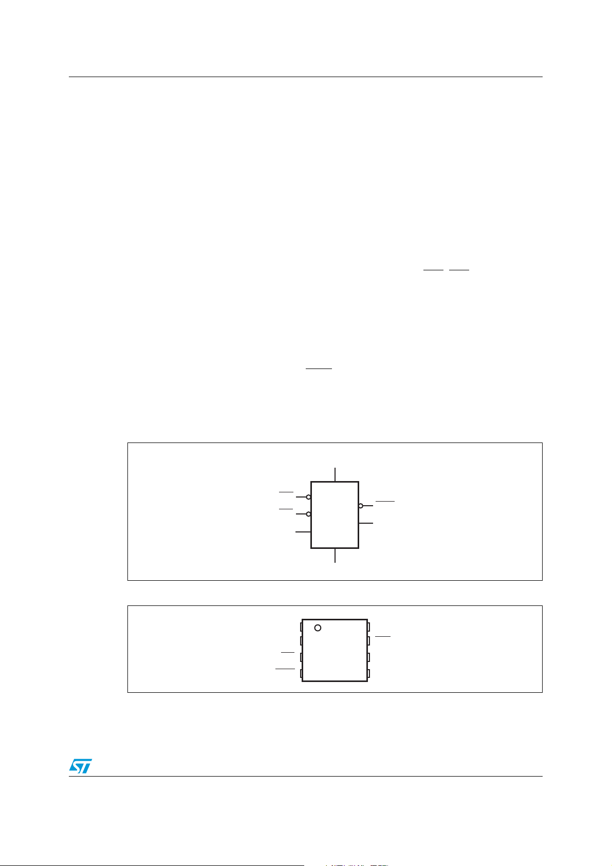
Figure 1. Logic diagram
V
CC
SR0
SR1
DSR
STM6520
V
SS
RST1
RST2
AM00434
Figure 2. Pin connections
RST2
V
SS
SR1
RST1
1
2
STM6520
3
4
8
V
CC
SR0
7
NC
6
5
DSR
AM00435
Doc ID 15953 Rev 6 5/23
Page 6
Device overview STM6520
2 Device overview
Table 1. Signal names
Symbol Input/output Description
RST1
Output First reset output, active-low, open-drain.
RST2 Output Second reset output, active-high, push-pull.
SR0
SR1
Input Primary push-button Smart Reset™ input. Active-low.
Input Secondary push-button Smart Reset™ input. Active-low.
A dual-state Smart Reset™ input delay selection pin. When
DSR Input
connected to ground, t
t
= 12.5 s (typ.). DSR is a DC-type input, intended to be either
SRC
= 7.5 s; when connected to VCC,
SRC
permanently grounded or permanently connected to V
Positive supply voltage for the device. A 0.1 µF decoupling ceramic
V
CC
Supply voltage
capacitor is recommended to be connected between VCC and VSS
pins.
V
SS
Supply ground Ground
NC No connect (not bonded; should be connected to V
SS
.
CC
).
6/23 Doc ID 15953 Rev 6
Page 7
STM6520 Pin descriptions
3 Pin descriptions
3.1 Power supply (VCC)
This pin is used to provide power to the Smart Reset™ device. A 0.1 µF ceramic decoupling
capacitor is recommended to be connected between the V
STM6520 device as possible.
3.2 Ground (VSS)
This is the ground pin for the device.
3.3 Smart Reset™ inputs (SR0, SR1)
Push-button Smart Reset™ inputs, active-low. Both inputs need to be asserted
simultaneously for at least t
to activate the reset outputs.
SRC
3.4 User-selectable Smart Reset™ delay (DSR)
and VSS pins, as close to the
CC
An input that allows the user to program the setup time (t
buttons need to be pressed to activate the reset outputs. Controlled by different voltage
levels on the DSR pin: when connected to ground, t
t
= 12.5 s (typ.). DSR is a DC-type input, intended to be either permanently grounded or
SRC
permanently connected to V
CC
.
3.5 Reset outputs (RST1, RST2)
RST1 is active-low, open-drain, RST2 active-high, push-pull. Neither fixed nor minimum
output reset pulse duration, nor power-on reset is implemented. Releasing any of the pushbuttons while reset outputs are active, causes both outputs to deassert.
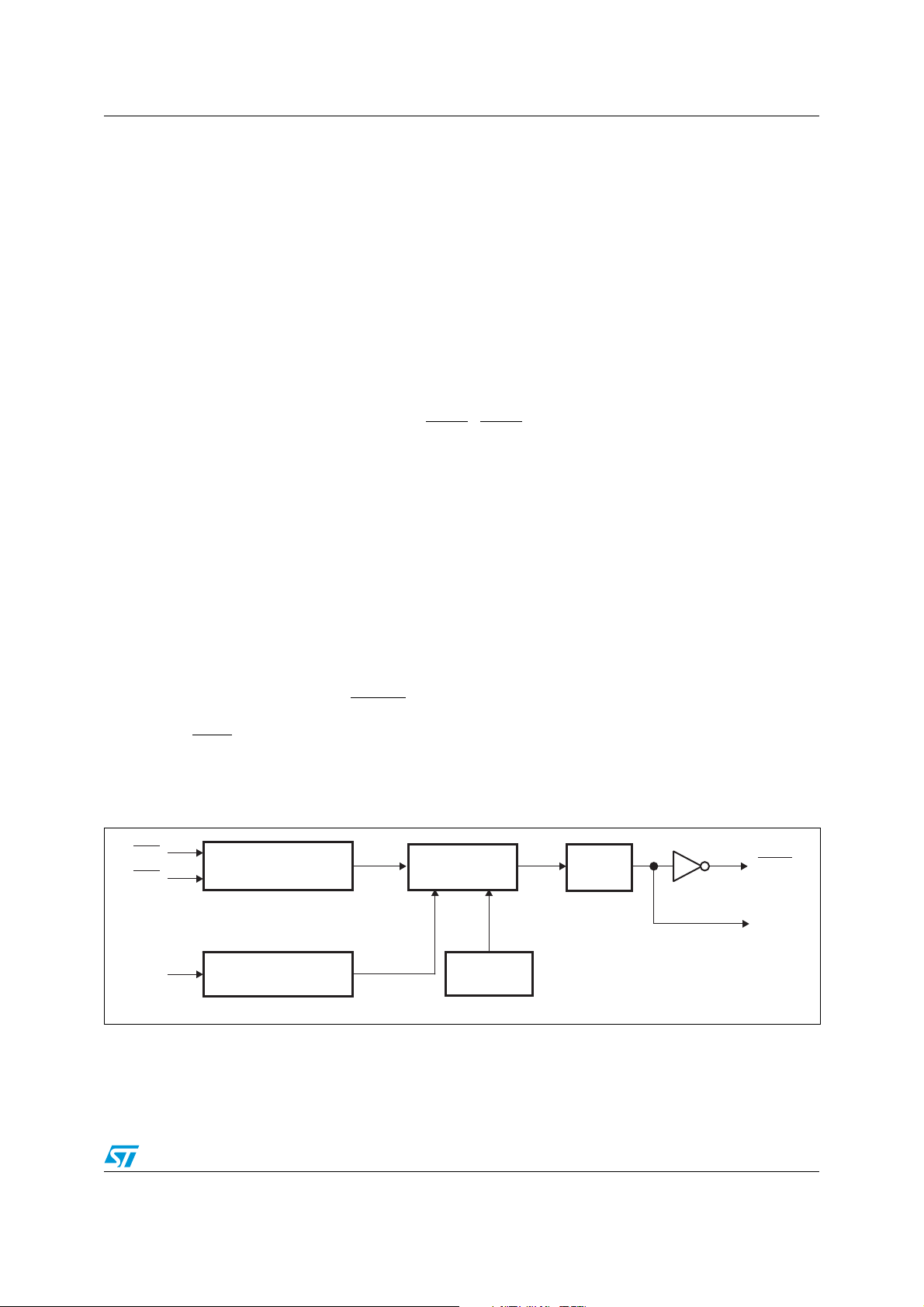
Figure 3. Block diagram
SR0
SR0
SR1
SR1
DSR
DSR
Smart ResetTM
Smart ResetTM
reset logic
reset logic
t
selector
t
selector
SRC
SRC
two-state logic
two-state logic
t
t
SRC
SRC
Oscillator
Oscillator
) for which both the push-
SRC
= 7.5 s, when connected to VCC,
SRC
Output
Output
logic
logic
RST1
RST1
RST2
RST2
AM00436V2
AM00436V2
Doc ID 15953 Rev 6 7/23
Page 8

Typical application diagram STM6520
4 Typical application diagram
Figure 4. RST1 output used for microcontroller reset
V
BAT
C1
0.1 µF
STM6520
(1)
DSR
SR0
SR1 RST1
(2)
RST2
Sys_Reset
Reset
Power_on
Powerkey
System ASIC MCU
1. DSR pin (pin 5) must be tied to VCC or VSS.
2. When only one Smart Reset™ input is used, connect the unused one permanently to V
Figure 5. RST2 used for interrupting system power
System power
output
V
SYS
C1
0.1 µF
V
BAT
Regulator
EN
STM6520
(1)
DSR
SR0
SR1 RST1
(2)
RST2
Sys_Reset
Power_on
Powerkey
System ASIC MCU
SS
AM00440c
.
V
SYS
AM00439c
1. DSR pin (pin 5) must be tied to VCC or VSS.
2. When only one Smart Reset™ input is used, connect the unused one permanently to V
8/23 Doc ID 15953 Rev 6
SS
.
Page 9
STM6520 Typical application diagram
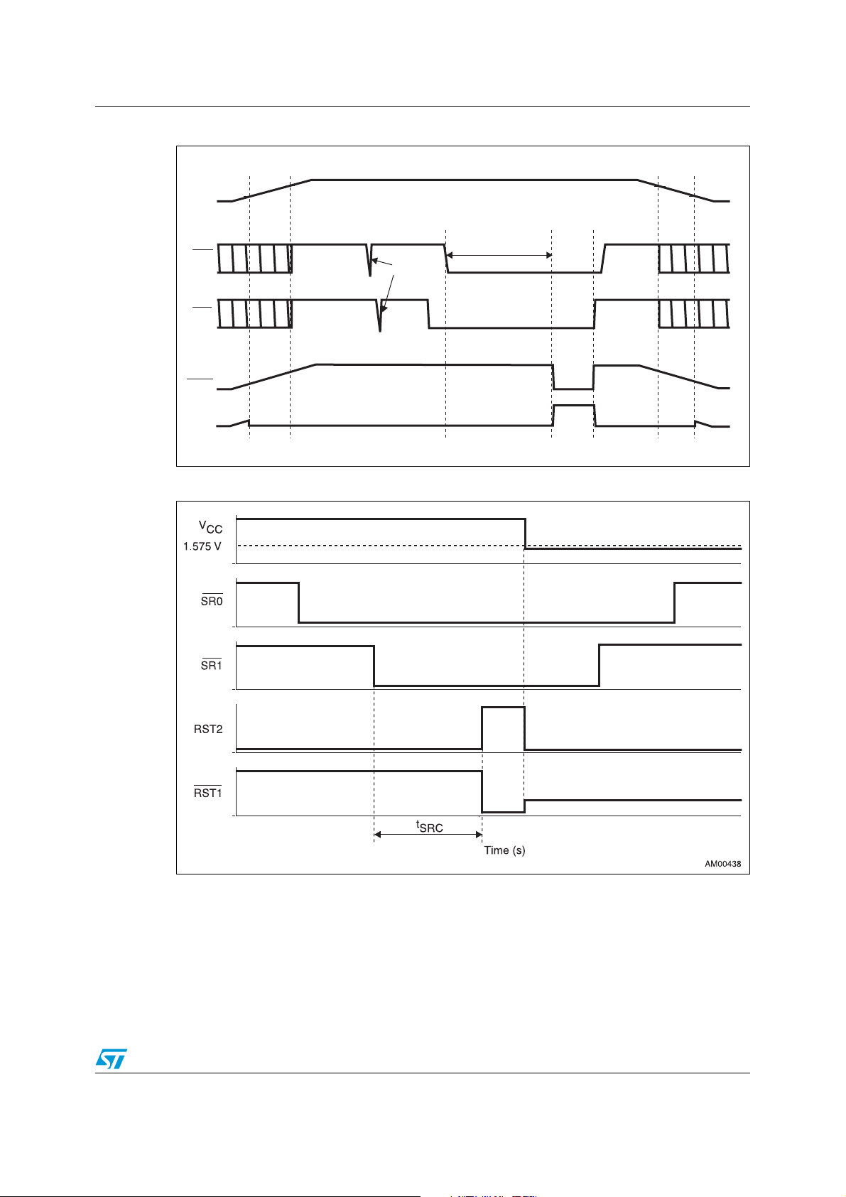
Figure 6. Timing waveforms
1.65 V
1.0 V
V
BAT
SR0
immunity
SR1
RST1
RST2
Figure 7. Undervoltage condition
5 V
0 V
5 V
Glitch
Start
timer
N seconds
t
SRC
End
timer
controlled output
1.65 V
1.0 V
Push-button
AM00437
0 V
5 V
0 V
5 V
0 V
5 V
0 V
Note: If undervoltage occurs (V
outputs are released and go inactive.
drops below 1.575 V typ.) while reset outputs are active, both
CC
Doc ID 15953 Rev 6 9/23
Page 10

Typical operating characteristics STM6520
5 Typical operating characteristics
Figure 8. Supply current (ICC) vs. temperature
3
2.5
2
ICC [µA]
1.5
1
0.5
0
–40 –20 0 20 40 60 80 100 120 140
Figure 9. Smart Reset™ delay (t
9
8.5
8
Temperature [˚C]
5.5 V 3.3 V 2 V
) vs. temperature, DSR = VSS
SRC
AM00624
t
[s]
SRC
–40 –20 0 20 40 60 80 100 120 140
7.5
7
6.5
6
Temperature [˚C]
5.5 V 3.3 V 2 V
10/23 Doc ID 15953 Rev 6
AM00625
Page 11
STM6520 Maximum rating
6 Maximum rating
Stressing the device above the rating listed in the “Absolute maximum ratings” table may
cause permanent damage to the device. These are stress ratings only and operation of the
device at these or any other conditions above those indicated in the operating sections of
this specification is not implied. Exposure to absolute maximum rating conditions for
extended periods may affect device reliability. Refer also to the STMicroelectronics SURE
Program and other relevant quality documents.
Table 2. Absolute maximum ratings
Symbol Parameter Value Unit
T
T
SLD
θ
V
V
STG
Storage temperature (VCC off) –55 to +150 °C
(1)
Lead solder temperature for 10 seconds 260 °C
Thermal resistance (junction to ambient) TDFN8 149.0 °C/W
JA
Input or output voltage –0.3 to 5.5
IO
Supply voltage –0.3 to 7 V
CC
ESD
V
HBM
V
RCDM
V
MM
1. Reflow at peak temperature of 260 °C. The time above 255 °C must not exceed 30 seconds.
2. For RST2 –0.3 to V
Electrostatic discharge protection, human body model,
all pins (JESD22-A114-B level 2)
Electrostatic discharge protection, charged device model,
all pins
Electrostatic discharge protection, machine model, all pins
(JESD22-A115-A level A)
Latch-up (V
pin, reset input pins) EIA/JESD78
CC
+0.3 V only.
CC
2kV
1kV
200 V
(2)
V
Doc ID 15953 Rev 6 11/23
Page 12
DC and AC parameters STM6520
7 DC and AC parameters
This section summarizes the operating measurement conditions, and the DC and AC
characteristics of the device. The parameters in the DC and AC characteristics table that
follow, are derived from tests performed under the Measurement Conditions summarized in
Table 3: Operating and measurement conditions. Designers should check that the operating
conditions in their circuit match the operating conditions when relying on the quoted
parameters.
Table 3. Operating and measurement conditions
Parameter Value Unit
V
supply voltage 1.65 to 5.5 V
CC
Ambient operating temperature (T
Input rise and fall times ≤
Input pulse voltages 0.2 to 0.8 V
Input and output timing ref. voltages 0.3 to 0.7 V
) –30 to +85 °C
A
5ns
CC
CC
V
V
Figure 10. AC testing input/output waveforms
0.8 V
CC
0.2 V
CC
0.7 V
0.3 V
CC
CC
AM00478
12/23 Doc ID 15953 Rev 6
Page 13
STM6520 DC and AC parameters
Table 4. DC and AC characteristics
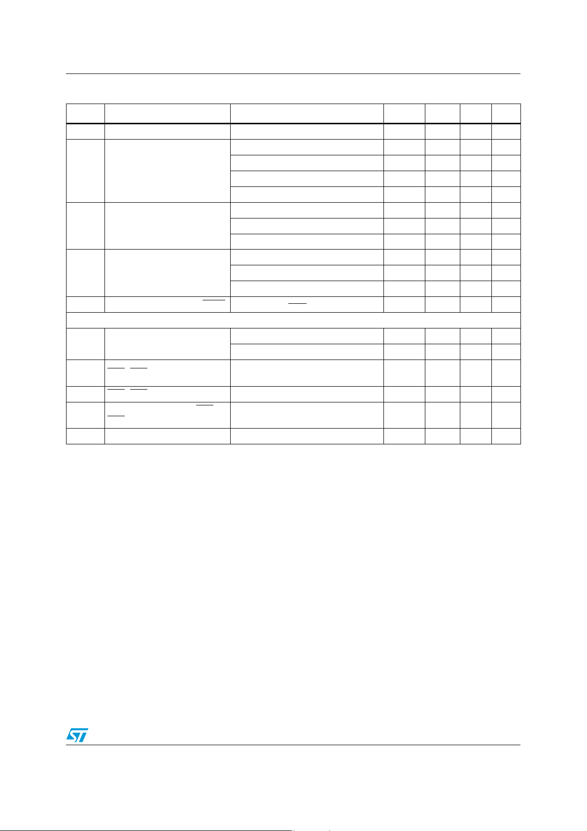
Symbol Parameter Test conditions
V
CC
I
CC
V
OL
V
OH
I
LO
Smart Reset
t
SRC
V
IL
V
IH
I
LI
1. Valid for ambient operating temperature: TA = –30 to +85 °C; VCC = 1.65 to 5.5 V (except where noted).
2. Typical value is at 25 °C and V
3. Reset outputs are deasserted below 1.575 V typ. and remain deasserted down to V
4. Input glitch immunity is equal to t
Supply voltage range Operating voltage
= 3.0 V, t
V
CC
V
= 5.0 V, t
Supply voltage
Reset output voltage low
Reset output voltage high,
RST2
CC
V
CC
V
CC
V
CC
V
CC
V
CC
V
CC
V
CC
V
CC
= 3.0 V, t
= 5.0 V, t
≥
≥
≥
≥
≥
≥
Output leakage current, RST1 Open-drain, V
™
Smart Reset™ delay
DSR = V
DSR = V
SRC
SRC
SRC
SRC
4.5 V, sinking 3.2 mA 0.3 V
3.3 V, sinking 2.5 mA 0.3 V
1.65 V, sinking 1 mA 0.3 V
4.5 V, I
SOURCE
2.7 V, I
SOURCE
1.65 V, I
RST1
SS
CC
SR0, SR1 input voltage low
(1)
(3)
counter is inactive 1.5 2.5 µA
counter is inactive 2.0 3.0 µA
counter is active 3.5 µA
counter is active 4.7 µA
= 0.8 mA 0.8 V
= 0.5 mA 0.8 V
SOURCE
= 0.25 mA 0.8 V
= 5.5 V –0.1 0.1 µA
Min. Typ.
1.65 5.5 V
CC
CC
CC
67.59s
10 12.5 15 s
V
SS
– 0.3
SR0, SR1 input voltage high 0.85 5.5 V
Input leakage current (SR0,
SR1
, DSR pins)
Input glitch immunity
(4)
= 3.3 V unless otherwise noted.
CC
(when both SR inputs are low), otherwise infinite.
SRC
Corresponds to the actual t
SRC
–1 1 µA
= 1 V.
CC
t
SRC
(2)
Max. Units
0.3 V
V
V
V
s
Doc ID 15953 Rev 6 13/23
Page 14

Package mechanical data STM6520
8 Package mechanical data
In order to meet environmental requirements, ST offers these devices in different grades of
ECOPACK
specifications, grade definitions and product status are available at: www.st.com.
ECOPACK
®
packages, depending on their level of environmental compliance. ECOPACK®
®
is an ST trademark.
Figure 11. TDFN - 8-lead, 2 x 2 mm package outline
PIN 1 INDEX AREA
0.10 C
0.10
C
A
0.08 C
PIN 1 INDEX AREA
D
2x
0.10 C
2x
TOP VIEW
SIDE VIEW
e
1
A
B
E
C
A1
SEATING
PLANE
b
4
0.10 C A B
Pin#1 ID
8
BOTTOM VIEW
14/23 Doc ID 15953 Rev 6
L
5
8070540_A
Page 15
STM6520 Package mechanical data
Table 5. TDFN – 8-lead 2 x 2 x 0.75 mm, 0.5 mm package mechanical data
Dimension (mm) Dimension (inches)
Symbol
Min. Nom. Max. Min. Nom. Max.
A 0.70 0.75 0.80 0.028 0.030 0.031
A1 0.00 0.02 0.05 0.000 0.001 0.002
b 0.15 0.20 0.25 0.006 0.008 0.010
D
BSC
E
BSC
1.9 2.00 2.1 0.075 0.079 0.083
1.9 2.00 2.1 0.075 0.079 0.083
e 0.50 0.020
L 0.45 0.55 0.65 0.018 0.022 0.026
Doc ID 15953 Rev 6 15/23
Page 16

Package footprint STM6520
9 Package footprint
Figure 12. Landing pattern - TDFN – 8-lead 2 x 2 mm without thermal pad
D
P
E1E
L
b
Table 6. Parameter for landing pattern - TDFN – 8-lead 2 x 2 mm package
Dimension (mm)
Parameter Description
Min. Nom. Max.
L Contact length 1.05
b Contact width 0.25
E Max. land pattern Y-direction
— 2.85 —
—
— 0.30
E1 Contact gap spacing — 0.65 —
D Max. land pattern X-direction — 1.75 —
P Contact pitch — 0.5 —
AM00441
1.15
16/23 Doc ID 15953 Rev 6
Page 17

STM6520 Tape and reel information
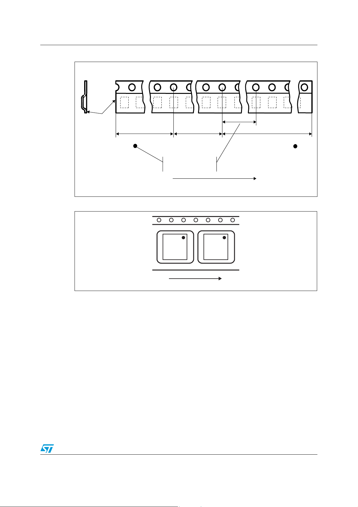
10 Tape and reel information
Figure 13. Carrier tape
P
0
D
T
Top cover
tape
K
0
Center lines
of cavity
Table 7. Carrier tape dimensions
Package W D E P
1.50
+0.10/
–0.00
1.75
±0.10
TDFN8
8.00
+0.30
–0.10
0
4.00
±0.10
P
2
User direction of feed
P
2.00
±0.10
FA0B
2
3.50
±0.05
±0.05
2.30
E
A
0
B
0
P
1
K
0
2.30
±0.05
1.00
±0.05
F
W
AM03073v2
P
0
4.00
±0.10
1
TUnit
0.250
±0.05
Bulk
qty.
mm 3000
Doc ID 15953 Rev 6 17/23
Page 18

Tape and reel information STM6520
Figure 14. Reel dimensions
T
40 mm min.
acces hole
at slot location
B
D
A
Full radius
C
N
Tape slot
in core for
tape start
25 mm min width
G measured
at hub
AM00443
Table 8. Reel dimensions
Tape sizes A max. B min. C D min. N min. G T max.
8 mm 180 (7 inches) 1.50 13.0 +/– 0.20 20.20 60 8.4 +2/–0 14.40
18/23 Doc ID 15953 Rev 6
Page 19
STM6520 Tape and reel information
Figure 15. Tape trailer/leader
End
To p
cover
tape
No components No componentsComponents
TRAILER
160 mm min.
Figure 16. Pin 1 orientation
Sealed with cover tape
User direction of feed
10 0 mm min.
LEADE
400 mm min.
Start
R
AM00444
Note: 1 Drawings are not to scale.
2 All dimensions are in mm, unless otherwise noted.
User direction of feed
AM00442
Doc ID 15953 Rev 6 19/23
Page 20

Ordering information STM6520
11 Ordering information
Table 9. Ordering information scheme
Example: STM6520 A Q R R DG 9 F
Device type
STM6520
Reset (V
monitoring threshold) voltage V
CC
A = no VCC monitoring feature
Smart Reset™ setup delay (t
SRC
)
Q = 7.5 or 12.5 s typ., user-selected (two-state);
input comparator on SR0
, SR1, no input pull-ups
Outputs type
R = RST1
Reset pulse timeout period (t
R = push-button controlled (no defined t
active-low, open-drain, no pull-up; RST2 active-high, push-pull
)
REC
, no power-on reset)
REC
Package
DG = TDFN8 2 x 2 x 0.75 mm, 0.5 mm pitch
Temperature range
9 = –30 °C to +85 °C
RST
Shipping method
F = ECOPACK
®
package, tape and reel
For other options, voltage threshold values etc. or for more information on any aspect of this
device, please contact the ST sales office nearest you.
20/23 Doc ID 15953 Rev 6
Page 21

STM6520 Package marking information
12 Package marking information
Table 10. Package marking
Part number Package Topmark
STM6520AQRRDG9F TDFN8 2 x 2 x 0.75 mm, 0.5 mm pitch DRM
STM6520AQRRDG9F TDFN8 2 x 2 x 0.75 mm, 0.5 mm pitch ERM
Figure 17. Package marking area, top view
A
BC
E
D
Topmark
A = dot (pin 1 reference)
B = assembly plant (P)
C = assembly year (Y, 0-9): 9 = 2009 etc.
D = assembly work week (WW, 01 to 52): 20 = WW20 etc.
E = marking area (topmark)
AM00479
Doc ID 15953 Rev 6 21/23
Page 22

Revision history STM6520
13 Revision history
Table 11. Document revision history
Date Revision Changes
08-Jul-2009 1 Initial release.
Document reformatted, updated Section 1: Description,
20-Oct-2009 2
20-Jan-2010 3 Updated Section 1: Description, Ta b l e 1 .
06-May-2010 4 Updated title, Features, Applications, Ta b l e 5 .
31-May-2010 5
Ta ble 1 , Figure 4, Figure 5, Tab le 4 , renamed Section 2:
Device overview, added Section 5: Typical operating
characteristics, updated supply voltage range in Ta bl e 4 .
Replaced “smart reset” by “Smart Reset™”, updated
Applications, Section 1, Section 3.1, Section 3.5, Figure 4,
Figure 5, Ta b le 2 , Ta bl e 4 , Ta b l e 6 and Tab le 1 0.
06-Jan-2011 6 Updated I
- supply voltage in Ta b l e 4 .
CC
22/23 Doc ID 15953 Rev 6
Page 23

STM6520
y
Please Read Carefully:
Informatio n in this document is provided solely in connection with ST products. STMicroelectronics NV and its subsidiaries (“ST”) reserve the
right to make changes, corrections, modifications or improvements, to this document, and the products and services described herein at an
time, without notice.
All ST products are sold pursuant to ST’s terms and conditions of sale.
Purchasers are solely responsible for the choice, selection and use of the ST products and services described herein, and ST assumes no
liability whatsoever relating to the choice, selection or use of the ST products and services described herein.
No license, express or implied, by estoppel or otherwise, to any intellectual property rights is granted under this document. If any part of this
document refers to any third party products or services it shall not be deemed a license grant by ST for the use of such third party products
or services, or any intellectual property contained therein or considered as a warranty covering the use in any manner whatsoever of such
third party products or services or any intellectual property contained therein.
UNLESS OTHERWISE SET FORTH IN ST’S TERMS AND CONDITIONS OF SALE ST DISCLAIMS ANY EXPRESS OR IMPLIED
WARRANTY WITH RESPECT TO THE USE AND/OR SALE OF ST PRODUCTS INCLUDING WITHOUT LIMITATION IMPLIED
WARRANTIES OF MERCHANTABILITY, FITNESS FOR A PARTICULAR PURPOSE (AND THEIR EQUIVALENTS UNDER THE LAWS
OF ANY JURISDICTION), OR INFRINGEMENT OF ANY PATENT, COPYRIGHT OR OTHER INTELLECTUAL PROPERTY RIGHT.
UNLESS EXPRESSLY APPROVED IN WRITING BY AN AUTHORIZED ST REPRESENTATIVE, ST PRODUCTS ARE NOT
RECOMMENDED, AUTHORIZED OR WARRANTED FOR USE IN MILITARY, AIR CRAFT, SPACE, LIFE SAVING, OR LIFE SUSTAINING
APPLICATIONS, NOR IN PRODUCTS OR SYSTEMS WHERE FAILURE OR MALFUNCTION MAY RESULT IN PERSONAL INJURY,
DEATH, OR SEVERE PROPERTY OR ENVIRONMENTAL DAMAGE. ST PRODUCTS WHICH ARE NOT SPECIFIED AS "AUTOMOTIVE
GRADE" MAY ONLY BE USED IN AUTOMOTIVE APPLICATIONS AT USER’S OWN RISK.
Resale of ST products with provisions different from the statements and/or technical features set forth in this document shall immediately void
any warranty granted by ST for the ST product or service described herein and shall not create or extend in any manner whatsoever, any
liability of ST.
ST and the ST logo are trademarks or registered trademarks of ST in various countries.
Information in this document supersedes and replaces all information previously supplied.
The ST logo is a registered trademark of STMicroelectronics. All other names are the property of their respective owners.
© 2011 STMicroelectronics - All rights reserved
STMicroelectronics group of companies
Australia - Belgium - Brazil - Canada - China - Czech Republic - Finland - France - Germany - Hong Kong - India - Israel - Italy - Japan -
Malaysia - Malta - Morocco - Philippines - Singapore - Spain - Sweden - Switzerland - United Kingdom - United States of America
www.st.com
Doc ID 15953 Rev 6 23/23
 Loading...