

Reset
STM6513
Dual push-button Smart
TM
with dual reset outputs and user-selectable setup delay
Features
■ Dual Smart Reset push-button inputs with
user-selectable extended reset setup delay (by
three-state input logic): t
■ Capacitor-adjustable reset pulse duration
(t
)
REC1
■ Power-on reset
■ Dual reset output (RST1 is active-high, push-
pull type, RST2
■ Factory-programmable thresholds to monitor
V
in the range of 1.575 to 4.625 V typ.
CC
■ Operating voltage 1.0 V (active-low output
is active-low, open-drain)
valid) to 5.5 V
■ Low supply current 3 µA
■ Operating temperature: industrial grade –40 °C
to +85 °C
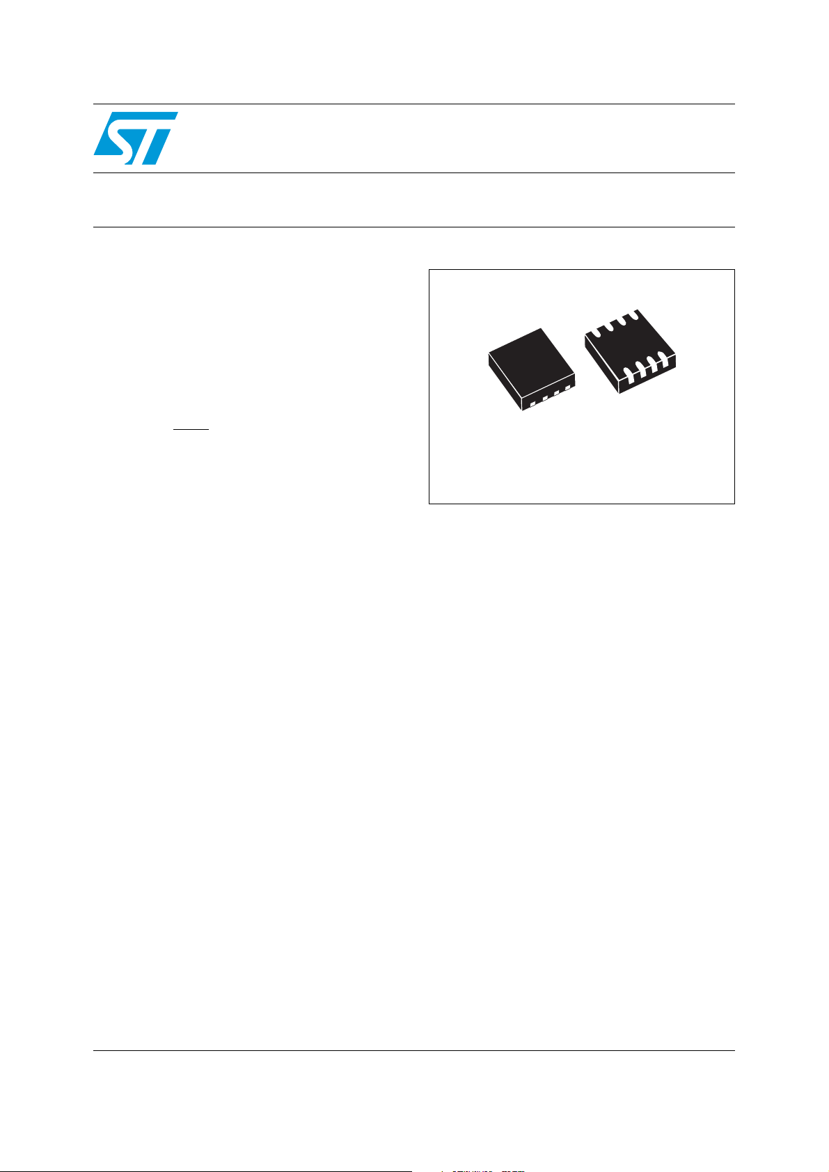
■ TDFN8 package: 2 mm x 2 mm x 0.75 mm
■ RoHS compliant
= 2, 6, 10 s (min.)
SRC
TDFN8 (DG)
2 mm x 2 mm
Applications
■ Mobile phones, smartphones
■ e-books
■ MP3 players
■ Games
■ Portable navigation devices
■ Any application that requires delayed reset
push-button(s) response for improved system
stability.
June 2010 Doc ID 16490 Rev 2 1/29
www.st.com
1

Contents STM6513
Contents
1 Description . . . . . . . . . . . . . . . . . . . . . . . . . . . . . . . . . . . . . . . . . . . . . . . . . 5
2 Device overview . . . . . . . . . . . . . . . . . . . . . . . . . . . . . . . . . . . . . . . . . . . . 7
3 Pin descriptions . . . . . . . . . . . . . . . . . . . . . . . . . . . . . . . . . . . . . . . . . . . . 8
3.1 Power supply (VCC) . . . . . . . . . . . . . . . . . . . . . . . . . . . . . . . . . . . . . . . . . . 8
3.2 Ground (V
3.3 Smart Reset inputs (SR0
3.4 User-programmable Smart Reset delay (TSR pin) . . . . . . . . . . . . . . . . . . 8
3.5 Reset outputs (RST1, RST2
3.6 Adjustable output reset timeout period input pin (TREC
) . . . . . . . . . . . . . . . . . . . . . . . . . . . . . . . . . . . . . . . . . . . . . . . 8
SS
, SR1) . . . . . . . . . . . . . . . . . . . . . . . . . . . . . . . . . 8
) . . . . . . . . . . . . . . . . . . . . . . . . . . . . . . . . . . . 8
) . . . . . . . . . . . 8
ADJ
4 Block diagram . . . . . . . . . . . . . . . . . . . . . . . . . . . . . . . . . . . . . . . . . . . . . 10
5 Typical operating characteristics . . . . . . . . . . . . . . . . . . . . . . . . . . . . . 12
6 Maximum rating . . . . . . . . . . . . . . . . . . . . . . . . . . . . . . . . . . . . . . . . . . . . 16
7 DC and AC parameters . . . . . . . . . . . . . . . . . . . . . . . . . . . . . . . . . . . . . . 17
8 Package mechanical data . . . . . . . . . . . . . . . . . . . . . . . . . . . . . . . . . . . . 20
9 Package footprint . . . . . . . . . . . . . . . . . . . . . . . . . . . . . . . . . . . . . . . . . . 22
10 Tape and reel information . . . . . . . . . . . . . . . . . . . . . . . . . . . . . . . . . . . . 23
11 Part numbering . . . . . . . . . . . . . . . . . . . . . . . . . . . . . . . . . . . . . . . . . . . . 26
12 Package marking information . . . . . . . . . . . . . . . . . . . . . . . . . . . . . . . . 27
13 Revision history . . . . . . . . . . . . . . . . . . . . . . . . . . . . . . . . . . . . . . . . . . . 28
2/29 Doc ID 16490 Rev 2

STM6513 List of tables
List of tables
Table 1. Signal names . . . . . . . . . . . . . . . . . . . . . . . . . . . . . . . . . . . . . . . . . . . . . . . . . . . . . . . . . . . . 7
Table 2. t
Table 3. Absolute maximum ratings . . . . . . . . . . . . . . . . . . . . . . . . . . . . . . . . . . . . . . . . . . . . . . . . . 16
Table 4. Operating and measurement conditions . . . . . . . . . . . . . . . . . . . . . . . . . . . . . . . . . . . . . . . 17
Table 5. DC and AC characteristics . . . . . . . . . . . . . . . . . . . . . . . . . . . . . . . . . . . . . . . . . . . . . . . . . 18
Table 6. Possible V
Table 7. TDFN – 8-lead 2 x 2 x 0.75 mm, 0.5 mm package mechanical data . . . . . . . . . . . . . . . . . 21
Table 8. Parameter for landing pattern - TDFN – 8-lead 2 x 2 mm package . . . . . . . . . . . . . . . . . . 22
Table 9. Carrier tape dimensions . . . . . . . . . . . . . . . . . . . . . . . . . . . . . . . . . . . . . . . . . . . . . . . . . . . 23
Table 10. Reel dimensions . . . . . . . . . . . . . . . . . . . . . . . . . . . . . . . . . . . . . . . . . . . . . . . . . . . . . . . . . 24
Table 11. Ordering information scheme . . . . . . . . . . . . . . . . . . . . . . . . . . . . . . . . . . . . . . . . . . . . . . . 26
Table 12. Package marking . . . . . . . . . . . . . . . . . . . . . . . . . . . . . . . . . . . . . . . . . . . . . . . . . . . . . . . . 27
Table 13. Document revision history . . . . . . . . . . . . . . . . . . . . . . . . . . . . . . . . . . . . . . . . . . . . . . . . . 28
programmed by an ideal external capacitor . . . . . . . . . . . . . . . . . . . . . . . . . . . . . . . . 9
REC1
voltage thresholds. . . . . . . . . . . . . . . . . . . . . . . . . . . . . . . . . . . . . . . . . . . . . 19
CC
Doc ID 16490 Rev 2 3/29

List of figures STM6513
List of figures
Figure 1. Logic diagram . . . . . . . . . . . . . . . . . . . . . . . . . . . . . . . . . . . . . . . . . . . . . . . . . . . . . . . . . . . . 6
Figure 2. Pin connections . . . . . . . . . . . . . . . . . . . . . . . . . . . . . . . . . . . . . . . . . . . . . . . . . . . . . . . . . . 6
Figure 3. Block diagram . . . . . . . . . . . . . . . . . . . . . . . . . . . . . . . . . . . . . . . . . . . . . . . . . . . . . . . . . . . 10
Figure 4. Typical application diagram . . . . . . . . . . . . . . . . . . . . . . . . . . . . . . . . . . . . . . . . . . . . . . . . 11
Figure 5. Timing waveforms. . . . . . . . . . . . . . . . . . . . . . . . . . . . . . . . . . . . . . . . . . . . . . . . . . . . . . . . 11
Figure 6. Smart Reset delay t
TSR = V
. . . . . . . . . . . . . . . . . . . . . . . . . . . . . . . . . . . . . . . . . . . . . . . . . . . . . . . . . . . . . 12
SS
Figure 7. Output reset timeout period t
(t
option E) . . . . . . . . . . . . . . . . . . . . . . . . . . . . . . . . . . . . . . . . . . . . . . . . . . . . . . . . . . 13
Figure 8. Supply current I
Figure 9. Reset voltage V
REC
CC
RST
(threshold option S, 2.925 V typ.) . . . . . . . . . . . . . . . . . . . . . . . . . . . . . . . . . . . . . . . . . . . . 14
Figure 10. Input leakage current, TSR pin, logic low vs. temperature and supply voltage V
Figure 11. Input leakage current, TSR pin, logic high vs. temperature and supply voltage V
Figure 12. AC testing input/output waveforms . . . . . . . . . . . . . . . . . . . . . . . . . . . . . . . . . . . . . . . . . . . 17
Figure 13. TDFN - 8-lead, 2 x 2 x 0.75 mm, 0.5 mm pitch. . . . . . . . . . . . . . . . . . . . . . . . . . . . . . . . . . 20
Figure 14. Landing pattern - TDFN – 8-lead 2 x 2 mm without thermal pad . . . . . . . . . . . . . . . . . . . . 22
Figure 15. Carrier tape . . . . . . . . . . . . . . . . . . . . . . . . . . . . . . . . . . . . . . . . . . . . . . . . . . . . . . . . . . . . 23
Figure 16. Reel dimensions . . . . . . . . . . . . . . . . . . . . . . . . . . . . . . . . . . . . . . . . . . . . . . . . . . . . . . . . . 24
Figure 17. Tape trailer/leader. . . . . . . . . . . . . . . . . . . . . . . . . . . . . . . . . . . . . . . . . . . . . . . . . . . . . . . . 25
Figure 18. Pin 1 orientation . . . . . . . . . . . . . . . . . . . . . . . . . . . . . . . . . . . . . . . . . . . . . . . . . . . . . . . . . 25
Figure 19. Package marking area, top view. . . . . . . . . . . . . . . . . . . . . . . . . . . . . . . . . . . . . . . . . . . . . 27
vs. temperature and supply voltage VCC,
SRC
vs. temperature and supply voltage VCC
REC2
vs. temperature and supply voltage VCC . . . . . . . . . . . . . . . . . . . . . . . 13
(falling) vs. temperature
. . . . . . 14
CC
. . . . . 15
CC
4/29 Doc ID 16490 Rev 2

STM6513 Description
1 Description
The STM6513 has two separate delayed Smart Reset inputs (SR0, SR1) which when taken
low simultaneously provide three user-selectable delayed Smart Reset setup time (t
options of 2 s, 6 s and 10 s. These are selected through a three-state TSR input pin: when
connected to ground, t
t
= 10 s (all the times are minimum). There are two reset outputs, both going active
SRC
= 2 s; when left open, t
SRC
= 6 s; when connected to VCC,
SRC
simultaneously after both the Smart Reset inputs were held active for the selected t
delay time. The first reset output, RST1, is active-high, push-pull; the second reset output,
RST2
, is active-low, open-drain requiring an external pull-up resistor. The duration of the
output reset pulses is independently programmable: t
external capacitor C
360 ms typ. Additionally, the V
tREC
), t
is factory-programmed to 210 ms (typ.), with the option of
REC2
is monitored and if it drops below the selected V
CC
threshold, both the reset outputs go active and remain so while V
threshold, plus the defined duration of the reset pulse t
is user-programmable (by
REC1
is below the V
CC
on each output.
REC
Smart Reset devices
The Smart Reset device family STM65xx provides a useful feature that ensures inadvertent
short reset push-button closures do not cause system resets. This is done by implementing
extended Smart Reset input delay (t
). Once the valid Smart Reset input levels and setup
SRC
delay are met, the device generates an output reset pulse with user-programmable timeout
period (t
REC
).
The Smart Reset inputs can be also connected to the applications interrupt to allow the
control of both the interrupt pin and the hard reset functions. If the push-buttons are closed
for a short time, the processor is only interrupted. If the system still does not respond
properly, holding the push-buttons for the extended setup time (t
) causes hard reset of
SRC
the processor through the reset outputs. The Smart Reset feature helps significantly
increase system stability.
SRC
RST
RST
SRC
)
The STM65xx family of Smart Reset devices consists of low current microprocessor reset
circuits targeted at applications such as MP3 players, navigation, smartphones or mobile
phones; generally any application that requires delayed reset push-button(s) response for
improved system stability. The STM65xx devices feature single or dual Smart Reset inputs
(SR). The delayed Smart Reset setup time (t
) options of 2 s, 6 s and 10 s
SRC
(all min.) are adjustable by an external capacitor on the SRC pin or selectable by three-state
logic. The delayed setup period ignores switch closures shorter than t
, thus preventing
SRC
unwanted resets.
The STM65xx devices have active-low (optionally active-high) open-drain reset (RST
)
output(s) with or without internal pull-up resistor or push-pull as output options, with factoryprogrammed or capacitor-adjustable or push-buttons defined output reset pulse duration,
with or without power-on reset function.
Some devices also have an undervoltage monitoring feature: the reset output is also
asserted when the monitored supply voltage V
reset output remains asserted for the reset timeout period (t
drops below the specified threshold. The
CC
) after the monitored supply
REC
voltage goes above the specified threshold.
Doc ID 16490 Rev 2 5/29
Description STM6513
Figure 1. Logic diagram
V
CC
SR1
TREC
ADJ
SR0
TSR
STM6513
V
SS
RST1
RST2
AM00372
Figure 2. Pin connections
RST1
V
SS
SR1
RST2
1
2
STM
6513
3
4
8
V
CC
7
SR0
TREC
6
5
ADJ
TSR
AM00373
6/29 Doc ID 16490 Rev 2
STM6513 Device overview
2 Device overview
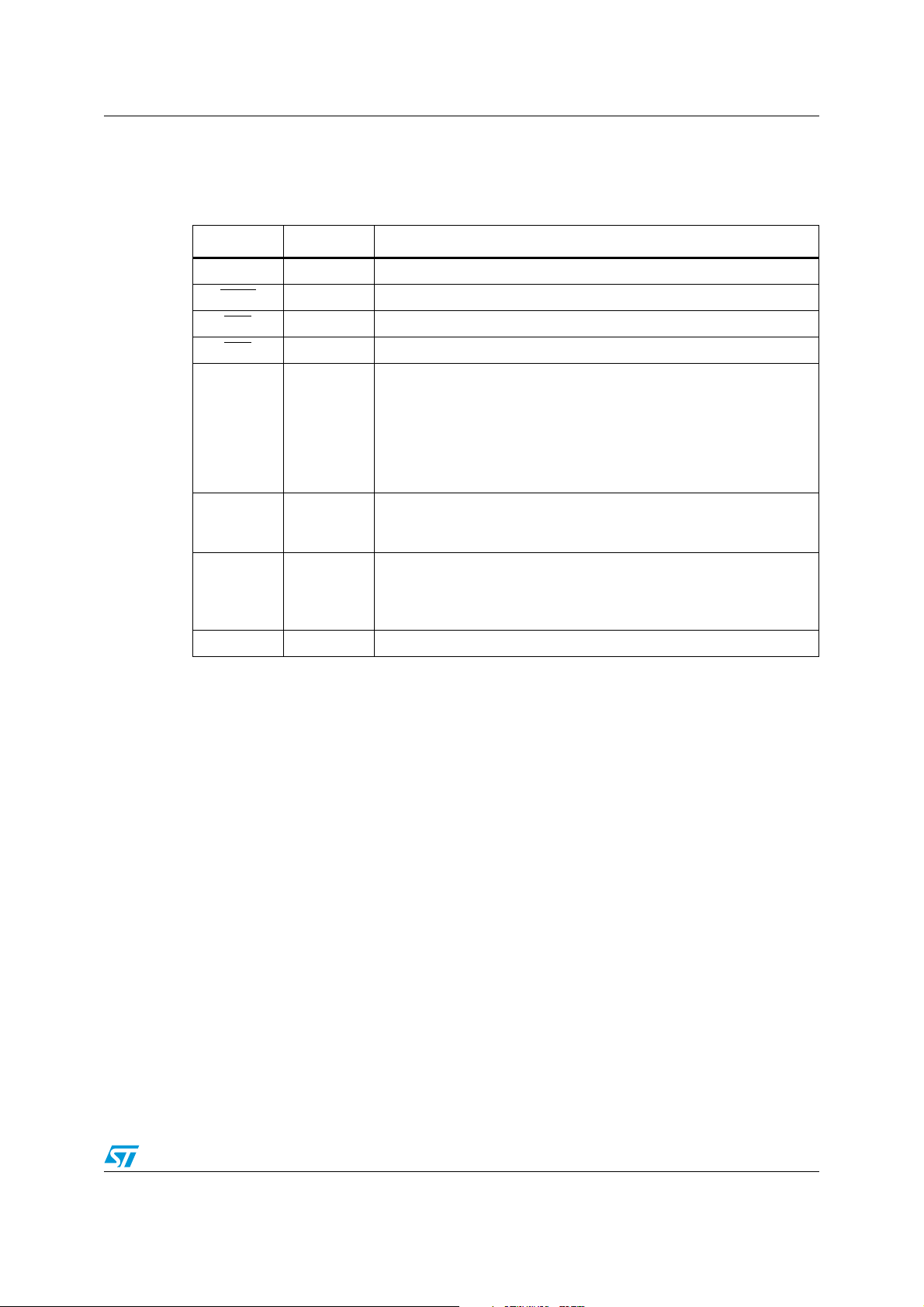
Table 1. Signal names
Symbol Input/output Description
RST1 Output First reset output, active-high, push-pull.
R
ST2 Output Second reset output, active-low, open-drain.
S
R0 Input Primary push-button Smart Reset input. Active-low.
S
R1 Input Secondary push-button Smart Reset input. Active-low.
A Three-state Smart Reset input delay setup control. When connected
TSR Input
TREC
ADJ
Input
to ground, t
V
, t
CC
SRC
intended to be either permanently grounded, permanently connected
to V
or permanently left open. If left open, for improved system glitch
CC
immunity it is strongly recommended to connect a 0.1 µF decoupling
ceramic capacitor between the TSR and V
Input pin for t
external capacitor C
programmed.
= 2 s; when left open, t
SRC
= 6 s; when connected to
SRC
= 10 s (all times are minimum). TSR is a DC-type input,
pins.
SS
reset pulse duration adjustment. Connect an
REC1
to this pin to determine t
tREC
REC1
; t
REC2
is factory-
Positive supply voltage input. Power supply for the device and an input
V
CC
Supply
for the monitored supply voltage. A 0.1 µF decoupling ceramic
capacitor is recommended to be connected between V
and VSS
CC
pins.
V
SS
Supply Ground
Doc ID 16490 Rev 2 7/29

Pin descriptions STM6513
3 Pin descriptions
3.1 Power supply (VCC)
This pin is used to provide the power to the Smart Reset device and to monitor the power
supply. A 0.1 µF decoupling ceramic capacitor is recommended to be connected between
V
and VSS pins.
CC
3.2 Ground (VSS)
This is the ground for the device and all supplies.
3.3 Smart Reset inputs (SR0, SR1)
Push-button Smart Reset inputs. Both inputs need to be held active at the same time for at
least t
the unused one permanently to V
to activate the reset outputs. When only one Smart Reset input is used, connect
SRC
SS
.
3.4 User-programmable Smart Reset delay (TSR pin)
Used to allow the user to program the setup time before the push-buttons action is validated
by reset output. Controlled by different voltage levels on the TSR pin: when connected to
ground, t
(all times are minimum). TSR is a DC-type input, intended to be either permanently
grounded, permanently connected to V
system glitch immunity it is strongly recommended to connect a 0.1 µF decoupling ceramic
capacitor between the TSR and V
= 2 s; when left open, t
SRC
= 6 s; when connected to VCC, t
SRC
or permanently left open. If left open, for improved
CC
pins.
SS
SRC
= 10 s
3.5 Reset outputs (RST1, RST2)
Reset outputs, RST1 active-high, push-pull type, RST2 active-low, open-drain.
3.6 Adjustable output reset timeout period input pin (TREC
The output reset timeout period (t
capacitor C
Ta bl e 2 . Refer also to Ta bl e 5.
to the TREC
tREC
ADJ
) on RST1 is adjustable by connecting an external
REC1
pin. Calculated t
REC
and C
examples are given in
tREC
ADJ
)
8/29 Doc ID 16490 Rev 2
STM6513 Pin descriptions
Table 2. t
C
value (µF)
tREC
programmed by an ideal external capacitor
REC1
(ms)
(1)(2)
t
REC1
Min. Typ. Max.
Closest common
value (µF)
C
tREC
0.001 10 15 20 0.001
0.002 20 30 40 0.0022
0.01 100 150 200 0.01
0.014 140 210 280 0.015
0.028 280 420 560 0.027
0.056 560 840 1120 0.056
0.112 1120 1680 2240 0.12
1. At 25 ° C. Example calculations based on an ideal capacitor. During application design and component
selection it should be considered that the current flowing into the external t
(C
) is on the order of 100 nA, therefore a low-leakage capacitor (ceramic or film capacitor) should be
tREC
used and placed as close as possible to the TREC
environment should be ensured to prevent t
value of C
2. In case of repeated activations of the internal t
intervals to fully discharge C
is 0.001 µF.
tREC
, so that the next t
tREC
REC
pin. Also an adequate low-leakage PCB
ADJ
accuracy from being affected. A recommended minimum
timer, an interval of 10 ms min. is needed between t
REC
is as specified.
REC1
programming capacitor
REC
REC
Doc ID 16490 Rev 2 9/29

Block diagram STM6513
4 Block diagram
Figure 3. Block diagram
SR1
SR0
TSR
V
SR logic
Three-state
selector
CC
V
REF
t
REC2
+
–
I
REF
t
SRC
t
REC1
Oscillator
TREC
ADJ
RST2
RST1
AM00374V2
10/29 Doc ID 16490 Rev 2

STM6513 Block diagram
STM6513 hookup with RST1 and RST2, bridging the PS_hold reset pulse during the
microprocessor reset initiated by the STM6513 Smart Reset device:
Figure 4. Typical application diagram
V
CC
PMU
LD00
LD07
Seq.
logic
V
REG
...
(PU resistor)
MCU
RST_n
POWER
KEY
C
tREC
TREC
TSR
ADJ
PWR
SW
V
STM6513
PS_hold
REG
Figure 5. Timing waveforms
POR initiated
SR0, SR1
RST1 (PP)
RST2 (OD)
SR0
SR1
100 kΩ
RST
PS_hold
GPIO1 GPIOn
Forces PS_hold
high during
reset period
Smart Reset™ initiated
t
SRC
KEYn
KEY1
AM00375a
RST2 (OD)
Factory programmed
RST1 (PP)
by C
tREC
t
REC1
t
REC2
(~1 s)
(210 ms)
t
REC1
t
REC2
(~1 s)
(210 ms)
AM00376V2
Doc ID 16490 Rev 2 11/29

Typical operating characteristics STM6513
5 Typical operating characteristics
Figure 6. Smart Reset delay t
t
SRC
TSR = V
[s]
–60 –40 –20 0 20 40 60 80 100 120 140
SS
3
2.9
2.8
2.7
2.6
2.5
2.4
2.3
2.2
2.1
2
vs. temperature and supply voltage VCC,
SRC
Temperature [˚C]
5.5 V 3.3 V
AM00632
12/29 Doc ID 16490 Rev 2

STM6513 Typical operating characteristics
Figure 7. Output reset timeout period t
V
(t
option E)
REC
280
260
240
220
200
180
160
140
t
REC2
CC
[ms]
–60 –40 –20 0 20 40 60 80 100 120 140
vs. temperature and supply voltage
REC2
Temperature [˚C]
5.5 V 3.3 V
AM00633
Figure 8. Supply current I
I
[µA]
CC
–60 –40 –20 0 20 40 60 80 100 120 140
vs. temperature and supply voltage V
CC
6
5
4
3
2
1
0
Temperature [˚C]
5.5 V 3.3 V
CC
AM00634
Doc ID 16490 Rev 2 13/29

Typical operating characteristics STM6513
Figure 9. Reset voltage V
(threshold option S, 2.925 V typ.)
V
,
falling [V]
RST
–60 –40 –20 0 20 40 60 80 100 120 140
(falling) vs. temperature
RST
2.96
2.95
2.94
2.93
2.92
2.91
2.9
2.89
Temperature [˚C]
AM00635
Figure 10. Input leakage current, TSR pin, logic low vs. temperature and supply
I
LI(TSR), LO
voltage V
[µA]
CC
10
8
6
4
2
–60 –40 –20 0 20 40 60 80 100 120 140
0
–2
–4
–6
–8
–10
Temperature [˚C]
5.5 V 3.3 V 2 V
14/29 Doc ID 16490 Rev 2
AM00636

STM6513 Typical operating characteristics
Figure 11. Input leakage current, TSR pin, logic high vs. temperature and supply
voltage V
CC
10
8
6
4
2
I
LI(TSR ), HI
[µA]
–60 –40 –20 0 20 40 60 80 100 120 140
0
–2
–4
–6
–8
–10
Temperature [˚C]
5.5 V 3.3 V 2 V
AM00637
Doc ID 16490 Rev 2 15/29

Maximum rating STM6513
6 Maximum rating
Stressing the device above the rating listed in the Table 3: Absolute maximum ratings may
cause permanent damage to the device. These are stress ratings only and operation of the
device at these or any other conditions above those indicated in the Operating sections of
this specification is not implied. Exposure to absolute maximum rating conditions for
extended periods may affect device reliability. Refer also to the STMicroelectronics SURE
Program and other relevant quality documents.
Table 3. Absolute maximum ratings
Symbol Parameter Value Unit
T
STG
T
SLD
θ
JA
V
IO
V
CC
1. Reflow at peak temperature of 260 °C. The time above 255 °C must not exceed 30 s.
2. For RST1 –0.3 to VCC +0.3 V only.
Storage temperature (VCC off) –55 to +150 °C
(1)
Lead solder temperature for 10 seconds 260 °C
Thermal resistance (junction to ambient) TDFN8 149.0 °C/W
Input or output voltage –0.3 to 5.5
Supply voltage –0.3 to 7 V
(2)
V
16/29 Doc ID 16490 Rev 2

STM6513 DC and AC parameters
7 DC and AC parameters
This section summarizes the operating measurement conditions, and the DC and AC
characteristics of the device. The parameters in the Table 5: DC and AC characteristics that
follow, are derived from tests performed under the Measurement Conditions summarized in
Table 4.: Operating and measurement conditions. Designers should check that the
operating conditions in their circuit match the operating conditions when relying on the
quoted parameters.
Table 4. Operating and measurement conditions
Parameter Value Unit
V
supply voltage 1.0 to 5.5 V
CC
Ambient operating temperature (T
Input rise and fall times ≤
Input pulse voltages 0.2 to 0.8 V
Input and output timing ref. voltages 0.3 to 0.7 V
Figure 12. AC testing input/output waveforms
) –40 to +85 °C
A
5ns
CC
CC
V
V
0.8 V
0.2 V
CC
CC
0.7 V
0.3 V
CC
CC
AM00478
Doc ID 16490 Rev 2 17/29

DC and AC parameters STM6513
Table 5. DC and AC characteristics
Symbol Parameter Test conditions
Reset output valid - active-low 1.0 5.5 V
V
V
V
V
Supply voltage range
CC
Supply current (VCC)
I
CC
Reset output voltage
OL
low
Reset output voltage
OH
high, RST1
Fixed voltage trip
point for V
RST
monitoring (refer to
Ta b le 6 )
CC
Reset output valid - active-high 1.2 5.5 V
V
= 3.0 V, TSR left open
CC
V
= 5.0 V, TSR left open 4 6 µA
CC
V
≥
4.5 V, sinking 3.2 mA 0.3 V
CC
V
≥
3.3 V, sinking 2.5 mA 0.3 V
CC
V
≥
1.0 V, sinking 0.1 mA 0.3 V
CC
V
≥
4.5 V, I
CC
V
≥
CC
V
≥
CC
2.7 V, I
1.2 V, I
SOURCE
SOURCE
SOURCE
–40 to +85 °C V
25 °C V
L, M 0.5%
HYST
Hysteresis of V
RST
T, S, R, Z, Y, W, V 1%
V
(1)
(3)
Min. Typ.
= 0.8 mA 0.8 V
= 0.5 mA 0.8 V
= 0.05 mA 0.8 V
–2.5% V
RST
–2.0% V
RST
CC
CC
CC
(2)
Max. Units
35µA
V
V
V
V
RST
RST
+2.5% V
RST
V
+2.0% V
RST
t
REC2
t
REC1
V
to reset delay
CC
(4)
Output reset timeout
period on RST2
,
factory-programmed
User-adjustable
output reset timeout
period on RST1
Refer to Ta bl e 2 .
VCC falling from (V
to (V
- 100 mV) at 10 mV/µs
RST
+ 100 mV)
RST
20 µs
Option E 140 210 280 ms
Option F 240 360 480 ms
10 000 x
C
tREC
(µF)
15 000 x
C
tREC
(µF)
20 000 x
C
tREC
(µF)
ms
18/29 Doc ID 16490 Rev 2
STM6513 DC and AC parameters
Table 5. DC and AC characteristics (continued)
Symbol Parameter Test conditions
Smart Reset inputs (SRx)
(1)
Min. Typ.
(2)
Max. Units
22.53s
10 12.5 15 s
V
–0.3 0.3 V
SS
0.7 V
CC
t
SRC
t
SRC
V
V
Smart Reset delay
SR0, SR1 input
IL
voltage low
SR0, SR1 input
IH
voltage high
Input glitch
immunity
(5)
TSR = V
SS
TSR = floating 6 7.5 9 s
TSR = V
Corresponds to the actual t
CC
SRC
Input leakage
I
LI(SR)
current (SR0
, SR1
–1 1 µA
pins)
I
LI(TSR)
1. Valid for ambient operating temperature: TA = –40 to +85 °C; VCC = 1.0 V to 5.5 V (except where noted).
2. Typical value is at 25 °C and V
3. For devices with V
4. Guaranteed by design.
5. Input glitch immunity is equal to t
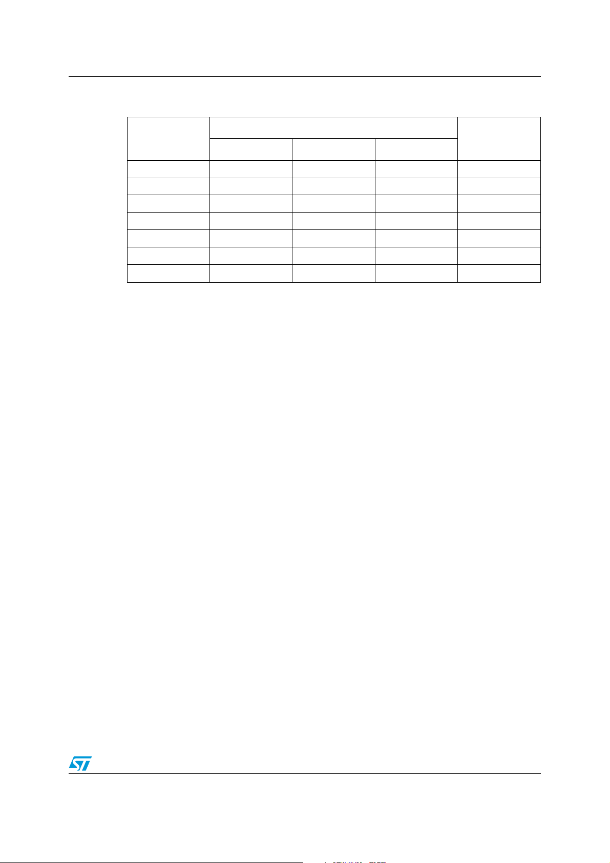
Table 6. Possible VCC voltage thresholds
Input leakage
current (TSR pin)
< 3.0 V.
RST
= 3.3 V unless otherwise noted.
CC
(when both SR inputs are low), otherwise infinite.
SRC
–5 7 µA
CC
5.5 V
V
s
VCC monitoring
threshold V
RST
Typ.
±2.5% (–40 °C to +85 °C) ±2.0% (25 °C)
Unit
Min. Max. Min. Max.
L (falling) 4.625 4.509 4.741 4.533 4.718 V
M (falling) 4.375 4.266 4.484 4.288 4.463 V
T (falling) 3.075 2.998 3.152 3.014 3.137 V
S (falling) 2.925 2.852 2.998 2.867 2.984 V
R (falling) 2.625 2.559 2.691 2.573 2.678 V
Z (falling) 2.313 2.255 2.371 2.267 2.359 V
Y (falling) 2.188 2.133 2.243 2.144 2.232 V
W (falling) 1.665 1.623 1.707 1.632 1.698 V
V (falling) 1.575 1.536 1.614 1.544 1.607 V
Doc ID 16490 Rev 2 19/29

Package mechanical data STM6513
8 Package mechanical data
In order to meet environmental requirements, ST offers these devices in different grades of
ECOPACK
specifications, grade definitions and product status are available at: www.st.com.
ECOPACK
®
packages, depending on their level of environmental compliance. ECOPACK®
®
is an ST trademark.
Figure 13. TDFN - 8-lead, 2 x 2 x 0.75 mm, 0.5 mm pitch
PIN 1 INDEX AREA
0.10 C
0.10
C
A
0.08 C
PIN 1 INDEX AREA
D
2x
0.10 C
2x
TOP VIEW
SIDE VIEW
e
1
A
B
E
C
A1
SEATING
PLANE
b
4
0.10 C A B
Pin#1 I D
8
BOTTOM VIEW
20/29 Doc ID 16490 Rev 2
L
5
TDFN-8L

STM6513 Package mechanical data
Table 7. TDFN – 8-lead 2 x 2 x 0.75 mm, 0.5 mm package mechanical data
Dimension (mm) Dimension (inches)
Symbol
Min. Nom. Max. Min. Nom. Max.
A 0.70 0.75 0.80 0.028 0.030 0.031
A1 0.00 0.02 0.05 0.000 0.001 0.002
b 0.15 0.20 0.25 0.006 0.008 0.010
D
BSC
E
BSC
1.9 2.00 2.1 0.075 0.079 0.083
1.9 2.00 2.1 0.075 0.079 0.083
e 0.50 0.020
L 0.45 0.55 0.65 0.018 0.022 0.026
Doc ID 16490 Rev 2 21/29
Package footprint STM6513
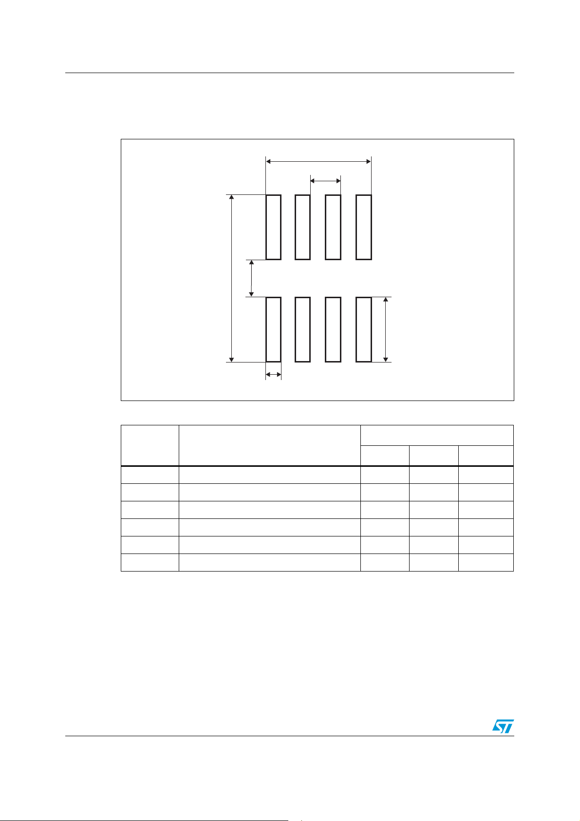
9 Package footprint
Figure 14. Landing pattern - TDFN – 8-lead 2 x 2 mm without thermal pad
D
P
E1E
L
b
Table 8. Parameter for landing pattern - TDFN – 8-lead 2 x 2 mm package
Dimension (mm)
Parameter Description
Min. Nom. Max.
L Contact length 1.05
b Contact width 0.25
E Max. land pattern Y-direction
E1 Contact gap spacing
D Max. land pattern X-direction
P Contact pitch
—
—
—
—
—
—
2.85
0.65
1.75
0.5
AM00441
1.15
0.30
—
—
—
—
22/29 Doc ID 16490 Rev 2
STM6513 Tape and reel information
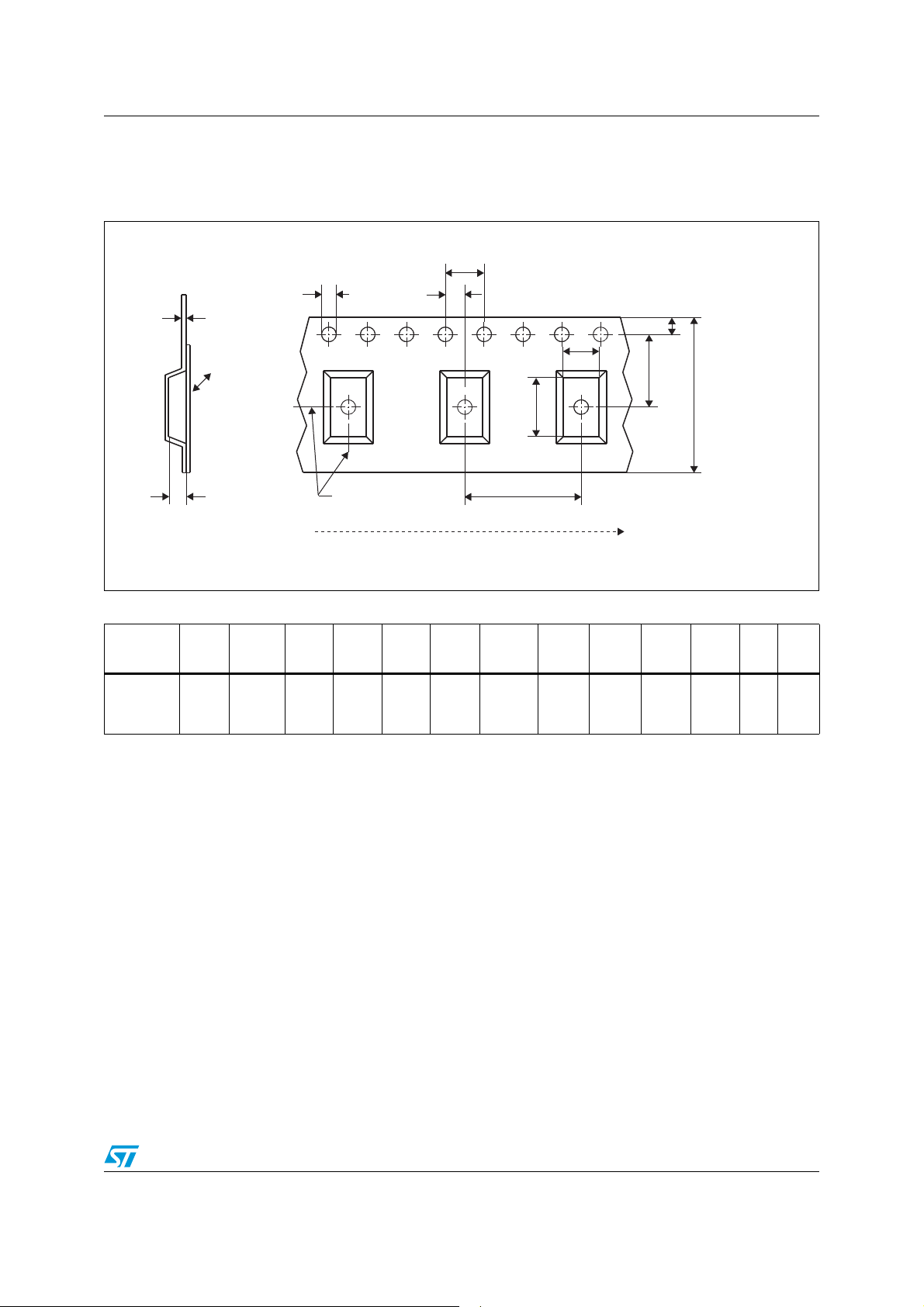
10 Tape and reel information
Figure 15. Carrier tape
P
0
D
T
Top c o ve r
tape
1.75
Center lines
of cavity
0
4.00
±0.10
K
0
Table 9. Carrier tape dimensions
Package W D E P
1.50
+0.10/
–0.00
±0.10
TDFN8
8.00
+0.30
–0.10
P
2
User direction of feed
P
2.00
±0.10
FA0B
2
3.50
±0.05
±0.05
2.30
E
A
0
B
0
P
1
K
0
2.30
±0.05
1.00
±0.05
F
W
AM03073v2
P
0
4.00
±0.10
1
0.250
±0.05
TUnit
Bulk
qty.
mm 3000
Doc ID 16490 Rev 2 23/29
Tape and reel information STM6513
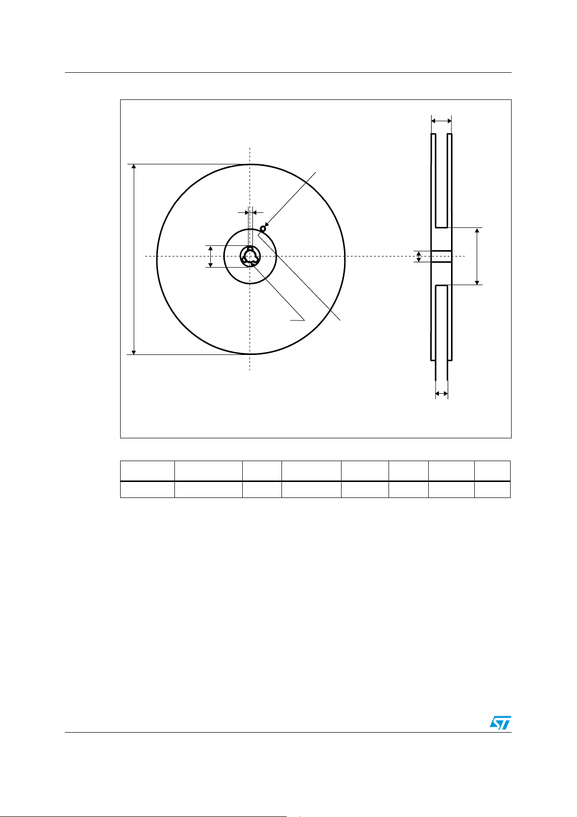
Figure 16. Reel dimensions
T
40 mm min.
acces hole
at slot location
B
D
A
Full radius
C
N
Tape slot
in core for
tape start
25 mm min width
G measured
at hub
AM00443
Table 10. Reel dimensions
Tape sizes A max. B min. C D min. N min. G T max.
8 mm 180 (7 inches) 1.50 13.0 +/– 0.20 20.20 60 8.4 +2/–0 14.40
24/29 Doc ID 16490 Rev 2
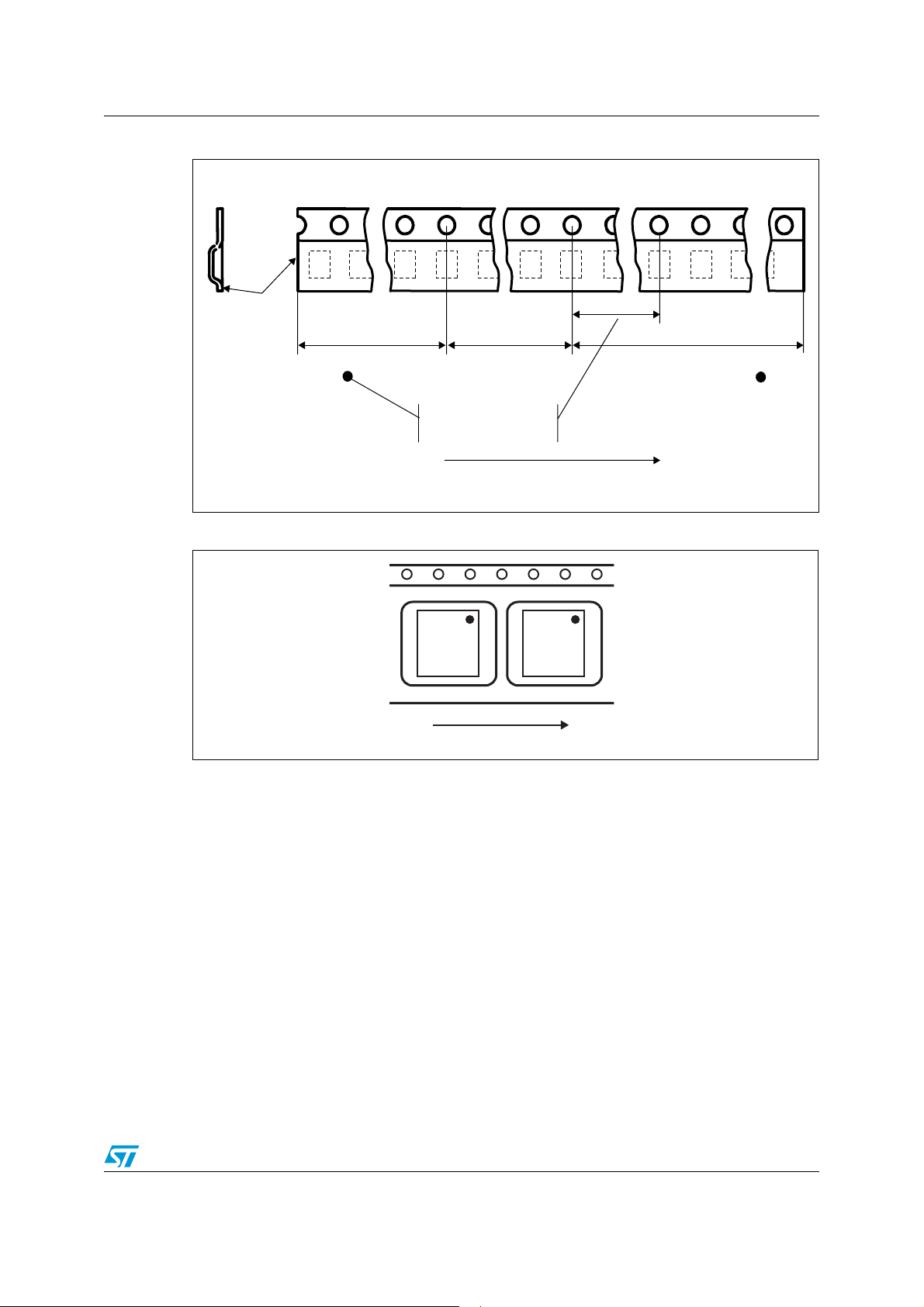
STM6513 Tape and reel information
Figure 17. Tape trailer/leader
End
To p
cover
tape
No components No componentsComponents
TRAILER
160 mm min.
Figure 18. Pin 1 orientation
Sealed with cover tape
User direction of feed
10 0 mm mi n.
LEADE
400 mm min.
Start
R
AM00444
Note: 1 Drawings are not to scale.
2 All dimensions are in mm, unless otherwise noted.
User direction of feed
AM00442
Doc ID 16490 Rev 2 25/29

Part numbering STM6513
11 Part numbering
Table 11. Ordering information scheme
Example: STM6513 V E I E DG 6 F
Device type
STM6513
Reset (V
monitoring threshold) voltage V
CC
RST
L = 4.625 V (typ., falling)
M = 4.375 V
T = 3.075 V
S = 2.925 V
R = 2.625 V
Z = 2.313 V
Y = 2.188 V
W = 1.665 V
V = 1.575 V
Smart Reset setup delay (t
presence of internal input pull-up on all Smart Reset inputs (SR0
SRC
);
, SR1)
E = 2 or 6 or 10 s min., user-programmed (three-state); no input pull-up
Outputs type
I = RST1 active-high, push-pull, RST2
Reset timeout period (t
E = t
F = t
user-programmable (external capacitor), t
REC1
user-programmable (external capacitor), t
REC1
REC
)
active-low, open-drain, no pull-up
factory-programmed (210 ms typ.)
REC2
factory-programmed (360 ms typ.)
REC2
Package
DG = TDFN8 - 2 x 2 x 0.75 mm, 0.5 mm pitch
Temperature range
6 = –40 °C to +85 °C
Shipping method
F = ECOPACK
®
package, tape and reel
For other options, voltage threshold values etc. or for more information on any aspect of this device,
please contact the ST sales office nearest you.
26/29 Doc ID 16490 Rev 2

STM6513 Package marking information
12 Package marking information
Table 12. Package marking
Full part number
STM6513VEIEDG6F TSR AL, NPU V AH, PP C
STM6513SEIEDG6F TSR AL, NPU S AH, PP C
STM6513REIEDG6F TSR AL, NPU R AH, PP C
Smart
t
SRC
delay
control
inputs type
Reset
V
RST
RST1
output
type
t
REC1
programming
tREC
tREC
tREC
RST2 output
type
t
REC2
option
Topmark
AL, OD, NPU E 9AH
AL, OD, NPU E 9SH
AL, OD, NPU E 9RH
Note: AL = active-low, AH = active-high; PP = push-pull, OD = open-drain, PU = internal pull-up
resistor, NPU = no internal pull-up resistor.
Figure 19. Package marking area, top view
A
BC
D
E
Topmark
A = dot (pin 1 reference)
B = assembly plant (P)
C = assembly year (Y, 0-9): 9 = 2009 etc.
D = assembly work week (WW, 01 to 52): 20 = WW20 etc.
E = marking area (topmark)
AM00479
Doc ID 16490 Rev 2 27/29

Revision history STM6513
13 Revision history
Table 13. Document revision history
Date Revision Changes
22-Oct-2009 1 Initial release.
Updated title, Features, Applications, replaced “smart reset” by
21-Jun-2010 2
“Smart Reset™” and “Smart Reset”, updated Section 1, Ta bl e 1 ,
Section 3, Ta bl e 2 , Figure 3, Figure 5, Figure 6, Ta b l e 3 , Ta bl e 5 to
Ta b le 8 , Ta b le 1 1 and Ta b le 1 2 .
28/29 Doc ID 16490 Rev 2

STM6513
y
Please Read Carefully:
Informatio n in this document is provided solely in connection with ST products. STMicroelectronics NV and its subsidiaries (“ST”) reserve the
right to make changes, corrections, modifications or improvements, to this document, and the products and services described herein at an
time, without notice.
All ST products are sold pursuant to ST’s terms and conditions of sale.
Purchasers are solely responsible for the choice, selection and use of the ST products and services described herein, and ST assumes no
liability whatsoever relating to the choice, selection or use of the ST products and services described herein.
No license, express or implied, by estoppel or otherwise, to any intellectual property rights is granted under this document. If any part of this
document refers to any third party products or services it shall not be deemed a license grant by ST for the use of such third party products
or services, or any intellectual property contained therein or considered as a warranty covering the use in any manner whatsoever of such
third party products or services or any intellectual property contained therein.
UNLESS OTHERWISE SET FORTH IN ST’S TERMS AND CONDITIONS OF SALE ST DISCLAIMS ANY EXPRESS OR IMPLIED
WARRANTY WITH RESPECT TO THE USE AND/OR SALE OF ST PRODUCTS INCLUDING WITHOUT LIMITATION IMPLIED
WARRANTIES OF MERCHANTABILITY, FITNESS FOR A PARTICULAR PURPOSE (AND THEIR EQUIVALENTS UNDER THE LAWS
OF ANY JURISDICTION), OR INFRINGEMENT OF ANY PATENT, COPYRIGHT OR OTHER INTELLECTUAL PROPERTY RIGHT.
UNLESS EXPRESSLY APPROVED IN WRITING BY AN AUTHORIZED ST REPRESENTATIVE, ST PRODUCTS ARE NOT
RECOMMENDED, AUTHORIZED OR WARRANTED FOR USE IN MILITARY, AIR CRAFT, SPACE, LIFE SAVING, OR LIFE SUSTAINING
APPLICATIONS, NOR IN PRODUCTS OR SYSTEMS WHERE FAILURE OR MALFUNCTION MAY RESULT IN PERSONAL INJURY,
DEATH, OR SEVERE PROPERTY OR ENVIRONMENTAL DAMAGE. ST PRODUCTS WHICH ARE NOT SPECIFIED AS "AUTOMOTIVE
GRADE" MAY ONLY BE USED IN AUTOMOTIVE APPLICATIONS AT USER’S OWN RISK.
Resale of ST products with provisions different from the statements and/or technical features set forth in this document shall immediately void
any warranty granted by ST for the ST product or service described herein and shall not create or extend in any manner whatsoe ver, any
liability of ST.
ST and the ST logo are trademarks or registered trademarks of ST in various countries.
Information in this document supersedes and replaces all information previously supplied.
The ST logo is a registered trademark of STMicroelectronics. All other names are the property of their respective owners.
© 2010 STMicroelectronics - All rights reserved
STMicroelectronics group of companies
Australia - Belgium - Brazil - Canada - China - Czech Republic - Finland - France - Germany - Hong Kong - India - Israel - Italy - Japan -
Malaysia - Malta - Morocco - Philippines - Singapore - Spain - Sweden - Switzerland - United Kingdom - United States of America
www.st.com
Doc ID 16490 Rev 2 29/29
 Loading...