

Page 1

High-performance, IEEE 802.15.4 wireless system-on-chip
VFQFPN48
(7 x 7 mm)
Features
■ Complete system-on-chip
– 32-bit ARM® Cortex™-M3 processor
– 2.4 GHz IEEE 802.15.4 transceiver & lower
MAC
– 8-Kbyte RAM and 64-Kbyte Flash memory
– AES128 encryption accelerator
– Flexible ADC, SPI/UART/I
communications, and general-purpose
timers
– 24 highly configurable GPIOs with Schmitt
trigger inputs
■ Industry-leading ARM® Cortex™-M3
processor
– Leading 32-bit processing performance
– Highly efficient Thumb®-2 instruction set
– Operation at 6, 12 or 24 MHz
– Flexible nested vectored interrupt controller
■ Low power consumption, advanced
management
– Receive current (w/ CPU): 27 mA
– Transmit current (w/ CPU, +3 dBm TX):
31 mA
– Low deep sleep current, with retained RAM
and GPIO: 400 nA/800 nA with/without
sleep timer
– Low-frequency internal RC oscillator for
low-power sleep timing
– High-frequency internal RC oscillator for
fast (100 µs) processor start-up from sleep
■ Exceptional RF performance
– Normal mode link budget up to 102 dB;
configurable up to 107 dB
– -99 dBm normal RX sensitivity;
configurable to -100 dBm (1% PER, 20
byte packet)
– +3 dB normal mode output power;
configurable up to +8 dBm
– Robust WiFi and Bluetooth coexistence
2
C serial
STM32W108C8
with 64-Kybte Flash memory
■ Innovative network and processor debug
– Non-intrusive hardware packet trace
– Serial wire/JTAG interface
– Standard ARM debug capabilities: Flash
patch and breakpoint; data watchpoint and
trace; instrumentation trace macrocell
■ Application flexibility
– Single voltage operation: 2.1-3.6 V with
internal 1.8 V and 1.25 V regulators
– Optional 32.768 kHz crystal for higher timer
accuracy
– Low external component count with single
24 MHz crystal
– Support for external power amplifier
– Small 7x7 mm 48-pin VFQFPN package
Applications
■ RF4CE products and remote controls
■ 6LoWPAN and custom protocols
■ 802.15.4 based network protocols (standard
and proprietary)
July 2011 Doc ID 018587 Rev 2 1/215
www.st.com
1
Page 2

STM32W108C8
1 Description . . . . . . . . . . . . . . . . . . . . . . . . . . . . . . . . . . . . . . . . . . . . . . . . 10
1.1 Development tools . . . . . . . . . . . . . . . . . . . . . . . . . . . . . . . . . . . . . . . . . . 11
1.2 Overview . . . . . . . . . . . . . . . . . . . . . . . . . . . . . . . . . . . . . . . . . . . . . . . . . 12
1.2.1 Functional description . . . . . . . . . . . . . . . . . . . . . . . . . . . . . . . . . . . . . . 12
1.2.2 ARM® Cortex™-M3 core . . . . . . . . . . . . . . . . . . . . . . . . . . . . . . . . . . . . 13
2 Documentation conventions . . . . . . . . . . . . . . . . . . . . . . . . . . . . . . . . . 14
3 Pinout and pin description . . . . . . . . . . . . . . . . . . . . . . . . . . . . . . . . . . . 15
4 Embedded memory . . . . . . . . . . . . . . . . . . . . . . . . . . . . . . . . . . . . . . . . . 26
4.1 Flash memory . . . . . . . . . . . . . . . . . . . . . . . . . . . . . . . . . . . . . . . . . . . . . 27
4.2 Random-access memory . . . . . . . . . . . . . . . . . . . . . . . . . . . . . . . . . . . . . 27
4.2.1 Direct memory access (DMA) to RAM . . . . . . . . . . . . . . . . . . . . . . . . . . 27
4.2.2 RAM memory protection . . . . . . . . . . . . . . . . . . . . . . . . . . . . . . . . . . . . 28
4.3 Memory protection unit . . . . . . . . . . . . . . . . . . . . . . . . . . . . . . . . . . . . . . . 28
5 Radio frequency module . . . . . . . . . . . . . . . . . . . . . . . . . . . . . . . . . . . . 29
5.1 Receive (Rx) path . . . . . . . . . . . . . . . . . . . . . . . . . . . . . . . . . . . . . . . . . . . 29
5.1.1 Rx baseband . . . . . . . . . . . . . . . . . . . . . . . . . . . . . . . . . . . . . . . . . . . . . 29
5.1.2 RSSI and CCA . . . . . . . . . . . . . . . . . . . . . . . . . . . . . . . . . . . . . . . . . . . . 29
5.2 Transmit (Tx) path . . . . . . . . . . . . . . . . . . . . . . . . . . . . . . . . . . . . . . . . . . 29
5.2.1 Tx baseband . . . . . . . . . . . . . . . . . . . . . . . . . . . . . . . . . . . . . . . . . . . . . 30
5.2.2 TX_ACTIVE and nTX_ACTIVE signals . . . . . . . . . . . . . . . . . . . . . . . . . 30
5.3 Calibration . . . . . . . . . . . . . . . . . . . . . . . . . . . . . . . . . . . . . . . . . . . . . . . . 30
5.4 Integrated MAC module . . . . . . . . . . . . . . . . . . . . . . . . . . . . . . . . . . . . . . 30
5.5 Packet trace interface (PTI) . . . . . . . . . . . . . . . . . . . . . . . . . . . . . . . . . . . 31
5.6 Random number generator . . . . . . . . . . . . . . . . . . . . . . . . . . . . . . . . . . . 31
6 System modules . . . . . . . . . . . . . . . . . . . . . . . . . . . . . . . . . . . . . . . . . . . 32
6.1 Power domains . . . . . . . . . . . . . . . . . . . . . . . . . . . . . . . . . . . . . . . . . . . . . 33
6.1.1 Internally regulated power . . . . . . . . . . . . . . . . . . . . . . . . . . . . . . . . . . . 33
6.1.2 Externally regulated power . . . . . . . . . . . . . . . . . . . . . . . . . . . . . . . . . . 33
6.2 Resets . . . . . . . . . . . . . . . . . . . . . . . . . . . . . . . . . . . . . . . . . . . . . . . . . . . 34
6.2.1 Reset sources . . . . . . . . . . . . . . . . . . . . . . . . . . . . . . . . . . . . . . . . . . . . 34
Watchdog reset . . . . . . . . . . . . . . . . . . . . . . . . . . . . . . . . . . . . . . . . . . . . . . . . . .34
1/215 Doc ID 018587 Rev 2
Page 3

STM32W108C8
6.3 Clocks . . . . . . . . . . . . . . . . . . . . . . . . . . . . . . . . . . . . . . . . . . . . . . . . . . . . 37
Software reset . . . . . . . . . . . . . . . . . . . . . . . . . . . . . . . . . . . . . . . . . . . . . . . . . . .34
Option byte error. . . . . . . . . . . . . . . . . . . . . . . . . . . . . . . . . . . . . . . . . . . . . . . . . .34
Debug reset . . . . . . . . . . . . . . . . . . . . . . . . . . . . . . . . . . . . . . . . . . . . . . . . . . . . .34
JTAG reset . . . . . . . . . . . . . . . . . . . . . . . . . . . . . . . . . . . . . . . . . . . . . . . . . . . . . .34
Deep sleep reset . . . . . . . . . . . . . . . . . . . . . . . . . . . . . . . . . . . . . . . . . . . . . . . . .35
6.2.2 Reset recording . . . . . . . . . . . . . . . . . . . . . . . . . . . . . . . . . . . . . . . . . . . 35
6.2.3 Reset generation . . . . . . . . . . . . . . . . . . . . . . . . . . . . . . . . . . . . . . . . . . 35
6.2.4 Reset register . . . . . . . . . . . . . . . . . . . . . . . . . . . . . . . . . . . . . . . . . . . . 36
Reset event source register (RESET_EVENT) . . . . . . . . . . . . . . . . . . . . . . . . . .36
6.3.1 High-frequency internal RC oscillator (OSCHF) . . . . . . . . . . . . . . . . . . 38
6.3.2 High-frequency crystal oscillator (OSC24M) . . . . . . . . . . . . . . . . . . . . . 39
6.3.3 Low-frequency internal RC oscillator (OSCRC) . . . . . . . . . . . . . . . . . . . 39
6.3.4 Low-frequency crystal oscillator (OSC32K) . . . . . . . . . . . . . . . . . . . . . . 39
6.3.5 Clock switching . . . . . . . . . . . . . . . . . . . . . . . . . . . . . . . . . . . . . . . . . . . 39
6.3.6 Clock switching registers . . . . . . . . . . . . . . . . . . . . . . . . . . . . . . . . . . . . 40
XTAL or OSCHF main clock select register (OSC24M_CTRL) . . . . . . . . . . . . . .40
CPU clock source select register (CPU_CLK_SEL). . . . . . . . . . . . . . . . . . . . . . .40
6.4 System timers . . . . . . . . . . . . . . . . . . . . . . . . . . . . . . . . . . . . . . . . . . . . . . 41
6.4.1 Watchdog timer . . . . . . . . . . . . . . . . . . . . . . . . . . . . . . . . . . . . . . . . . . . 41
6.4.2 Sleep timer . . . . . . . . . . . . . . . . . . . . . . . . . . . . . . . . . . . . . . . . . . . . . . . 41
6.4.3 Event timer . . . . . . . . . . . . . . . . . . . . . . . . . . . . . . . . . . . . . . . . . . . . . . . 42
6.4.4 Slow timers (Watchdog and Sleeptimer) control and status registers . . 42
Watchdog general control register (WDOG_CFG) . . . . . . . . . . . . . . . . . . . . . . . .42
Watchdog control register (WDOG_CTRL) . . . . . . . . . . . . . . . . . . . . . . . . . . . . .42
Watchdog restart register (WDOG_RESTART) . . . . . . . . . . . . . . . . . . . . . . . . . .43
Sleep timer configuration register (SLEEPTMR_CFG). . . . . . . . . . . . . . . . . . . . .43
Sleep timer count high register (SLEEPTMR_CNTH) . . . . . . . . . . . . . . . . . . . . .43
Sleep timer count low register (SLEEPTMR_CNTL) . . . . . . . . . . . . . . . . . . . . . .44
Sleep timer compare A high register (SLEEPTMR_CMPAH). . . . . . . . . . . . . . . .44
Sleep timer compare A low register (SLEEPTMR_CMPAL). . . . . . . . . . . . . . . . .45
Sleep timer compare B high register (SLEEPTMR_CMPBH). . . . . . . . . . . . . . . .45
Sleep timer compare B low register (SLEEPTMR_CMPBL). . . . . . . . . . . . . . . . .46
Sleep timer interrupt source register (INT_SLEEPTMRFLAG). . . . . . . . . . . . . . .46
Sleep timer interrupt mask register (INT_SLEEPTMRCFG). . . . . . . . . . . . . . . . .47
Sleep timer clock source enables (SLEEPTMR_CLKEN) . . . . . . . . . . . . . . . . . .47
6.5 Power management . . . . . . . . . . . . . . . . . . . . . . . . . . . . . . . . . . . . . . . . . 48
6.5.1 Wake sources . . . . . . . . . . . . . . . . . . . . . . . . . . . . . . . . . . . . . . . . . . . . 48
6.5.2 Basic sleep modes . . . . . . . . . . . . . . . . . . . . . . . . . . . . . . . . . . . . . . . . . 50
Doc ID 018587 Rev 2 2/215
Page 4

STM32W108C8
6.5.3 Further options for deep sleep . . . . . . . . . . . . . . . . . . . . . . . . . . . . . . . . 51
6.5.4 Use of debugger with sleep modes . . . . . . . . . . . . . . . . . . . . . . . . . . . . 51
6.6 Security accelerator . . . . . . . . . . . . . . . . . . . . . . . . . . . . . . . . . . . . . . . . . 52
7 Integrated voltage regulator . . . . . . . . . . . . . . . . . . . . . . . . . . . . . . . . . . 53
8 General-purpose input/outputs . . . . . . . . . . . . . . . . . . . . . . . . . . . . . . . 55
8.1 Functional description . . . . . . . . . . . . . . . . . . . . . . . . . . . . . . . . . . . . . . . 56
8.1.1 GPIO ports . . . . . . . . . . . . . . . . . . . . . . . . . . . . . . . . . . . . . . . . . . . . . . . 56
8.1.2 Configuration . . . . . . . . . . . . . . . . . . . . . . . . . . . . . . . . . . . . . . . . . . . . . 56
8.1.3 Forced functions . . . . . . . . . . . . . . . . . . . . . . . . . . . . . . . . . . . . . . . . . . 57
8.1.4 Reset . . . . . . . . . . . . . . . . . . . . . . . . . . . . . . . . . . . . . . . . . . . . . . . . . . . 58
8.1.5 nBOOTMODE . . . . . . . . . . . . . . . . . . . . . . . . . . . . . . . . . . . . . . . . . . . . 58
8.1.6 GPIO modes . . . . . . . . . . . . . . . . . . . . . . . . . . . . . . . . . . . . . . . . . . . . . 59
Analog mode . . . . . . . . . . . . . . . . . . . . . . . . . . . . . . . . . . . . . . . . . . . . . . . . . . . .59
Input mode . . . . . . . . . . . . . . . . . . . . . . . . . . . . . . . . . . . . . . . . . . . . . . . . . . . . . .59
Output mode. . . . . . . . . . . . . . . . . . . . . . . . . . . . . . . . . . . . . . . . . . . . . . . . . . . . .59
Alternate output mode . . . . . . . . . . . . . . . . . . . . . . . . . . . . . . . . . . . . . . . . . . . . .60
Alternate output SPI SCLK mode . . . . . . . . . . . . . . . . . . . . . . . . . . . . . . . . . . . . .60
8.1.7 Wake monitoring . . . . . . . . . . . . . . . . . . . . . . . . . . . . . . . . . . . . . . . . . . 60
8.2 External interrupts . . . . . . . . . . . . . . . . . . . . . . . . . . . . . . . . . . . . . . . . . . 61
8.3 Debug control and status . . . . . . . . . . . . . . . . . . . . . . . . . . . . . . . . . . . . . 62
8.4 GPIO alternate functions . . . . . . . . . . . . . . . . . . . . . . . . . . . . . . . . . . . . . 62
8.5 General-purpose input / output (GPIO) registers . . . . . . . . . . . . . . . . . . . 64
8.5.1 Port x configuration register (Low) (GPIO_PxCFGL) . . . . . . . . . . . . . . . 64
8.5.2 Port x configuration register (High) (GPIO_PxCFGH) . . . . . . . . . . . . . . 64
8.5.3 Port x input data register (GPIO_PxIN) . . . . . . . . . . . . . . . . . . . . . . . . . 65
8.5.4 Port x output data register (GPIO_PxOUT) . . . . . . . . . . . . . . . . . . . . . . 66
8.5.5 Port x output clear register (GPIO_PxCLR) . . . . . . . . . . . . . . . . . . . . . . 66
8.5.6 Port x output set register (GPIO_PxSET) . . . . . . . . . . . . . . . . . . . . . . . 67
8.5.7 Port x wakeup monitor register (GPIO_PxWAKE) . . . . . . . . . . . . . . . . . 67
8.5.8 GPIO wakeup filtering register (GPIO_WAKEFILT) . . . . . . . . . . . . . . . . 68
8.5.9 Interrupt x select register (GPIO_IRQxSEL) . . . . . . . . . . . . . . . . . . . . . 68
8.5.10 GPIO interrupt x configuration register (GPIO_INTCFGx) . . . . . . . . . . . 69
8.5.11 GPIO interrupt flag register (INT_GPIOFLAG) . . . . . . . . . . . . . . . . . . . 70
8.5.12 GPIO debug configuration register (GPIO_DBGCFG) . . . . . . . . . . . . . . 70
8.5.13 GPIO debug status register (GPIO_DBGSTAT) . . . . . . . . . . . . . . . . . . . 71
3/215 Doc ID 018587 Rev 2
Page 5

STM32W108C8
9 Serial interfaces . . . . . . . . . . . . . . . . . . . . . . . . . . . . . . . . . . . . . . . . . . . . 72
9.1 Functional description . . . . . . . . . . . . . . . . . . . . . . . . . . . . . . . . . . . . . . . 72
9.2 Configuration . . . . . . . . . . . . . . . . . . . . . . . . . . . . . . . . . . . . . . . . . . . . . . 73
9.3 SPI master mode . . . . . . . . . . . . . . . . . . . . . . . . . . . . . . . . . . . . . . . . . . . 74
9.3.1 Setup and configuration . . . . . . . . . . . . . . . . . . . . . . . . . . . . . . . . . . . . . 75
9.3.2 Operation . . . . . . . . . . . . . . . . . . . . . . . . . . . . . . . . . . . . . . . . . . . . . . . . 76
9.3.3 Interrupts . . . . . . . . . . . . . . . . . . . . . . . . . . . . . . . . . . . . . . . . . . . . . . . . 77
9.4 SPI slave mode . . . . . . . . . . . . . . . . . . . . . . . . . . . . . . . . . . . . . . . . . . . . 77
9.4.1 Setup and configuration . . . . . . . . . . . . . . . . . . . . . . . . . . . . . . . . . . . . . 78
9.4.2 Operation . . . . . . . . . . . . . . . . . . . . . . . . . . . . . . . . . . . . . . . . . . . . . . . . 79
9.4.3 DMA . . . . . . . . . . . . . . . . . . . . . . . . . . . . . . . . . . . . . . . . . . . . . . . . . . . . 80
9.4.4 Interrupts . . . . . . . . . . . . . . . . . . . . . . . . . . . . . . . . . . . . . . . . . . . . . . . . 80
9.5 Inter-integrated circuit interfaces (I2C) . . . . . . . . . . . . . . . . . . . . . . . . . . . 80
9.5.1 Setup and configuration . . . . . . . . . . . . . . . . . . . . . . . . . . . . . . . . . . . . . 81
9.5.2 Constructing frames . . . . . . . . . . . . . . . . . . . . . . . . . . . . . . . . . . . . . . . . 81
9.5.3 Interrupts . . . . . . . . . . . . . . . . . . . . . . . . . . . . . . . . . . . . . . . . . . . . . . . . 84
9.6 Universal asynchronous receiver / transmitter (UART) . . . . . . . . . . . . . . 84
9.6.1 Setup and configuration . . . . . . . . . . . . . . . . . . . . . . . . . . . . . . . . . . . . . 85
9.6.2 FIFOs . . . . . . . . . . . . . . . . . . . . . . . . . . . . . . . . . . . . . . . . . . . . . . . . . . . 86
9.6.3 RTS/CTS flow control . . . . . . . . . . . . . . . . . . . . . . . . . . . . . . . . . . . . . . 86
9.6.4 DMA . . . . . . . . . . . . . . . . . . . . . . . . . . . . . . . . . . . . . . . . . . . . . . . . . . . . 87
9.6.5 Interrupts . . . . . . . . . . . . . . . . . . . . . . . . . . . . . . . . . . . . . . . . . . . . . . . . 88
9.7 Direct memory access (DMA) channels . . . . . . . . . . . . . . . . . . . . . . . . . . 88
9.8 Serial controller registers . . . . . . . . . . . . . . . . . . . . . . . . . . . . . . . . . . . . . 89
9.8.1 Serial mode register (SCx_MODE) . . . . . . . . . . . . . . . . . . . . . . . . . . . . 89
9.8.2 Serial controller interrupt flag register (INT_SCxFLAG) . . . . . . . . . . . . 90
9.8.3 Serial controller interrupt configuration register (INT_SCxCFG) . . . . . . 91
9.8.4 Serial controller interrupt mode register (SCx_INTMODE) . . . . . . . . . . 92
9.9 SPI master mode registers . . . . . . . . . . . . . . . . . . . . . . . . . . . . . . . . . . . . 92
9.9.1 Serial data register (SCx_DATA) . . . . . . . . . . . . . . . . . . . . . . . . . . . . . . 92
9.9.2 SPI configuration register (SCx_SPICFG) . . . . . . . . . . . . . . . . . . . . . . . 93
9.9.3 SPI status register (SCx_SPISTAT) . . . . . . . . . . . . . . . . . . . . . . . . . . . . 94
9.9.4 Serial clock linear prescaler register (SCx_RATELIN) . . . . . . . . . . . . . . 94
9.9.5 Serial clock exponential prescaler register (SCx_RATEEXP) . . . . . . . . 95
9.10 SPI slave mode registers . . . . . . . . . . . . . . . . . . . . . . . . . . . . . . . . . . . . . 95
9.11 Inter-integrated circuit (I2C) interface registers . . . . . . . . . . . . . . . . . . . . 95
Doc ID 018587 Rev 2 4/215
Page 6

STM32W108C8
9.11.1 I2C status register (SCx_TWISTAT) . . . . . . . . . . . . . . . . . . . . . . . . . . . . 95
9.11.2 I2C control 1 register (SCx_TWICTRL1) . . . . . . . . . . . . . . . . . . . . . . . . 96
9.11.3 I2C control 2 register (SCx_TWICTRL2) . . . . . . . . . . . . . . . . . . . . . . . . 96
9.12 Universal asynchronous receiver / transmitter (UART) registers . . . . . . . 97
9.12.1 UART status register (SC1_UARTSTAT) . . . . . . . . . . . . . . . . . . . . . . . . 97
9.12.2 UART configuration register (SC1_UARTCFG) . . . . . . . . . . . . . . . . . . . 98
9.12.3 UART baud rate period register (SC1_UARTPER) . . . . . . . . . . . . . . . . 99
9.12.4 UART baud rate fractional period register (SC1_UARTFRAC) . . . . . . . 99
9.13 DMA channel registers . . . . . . . . . . . . . . . . . . . . . . . . . . . . . . . . . . . . . . 100
9.13.1 Serial DMA control register (SCx_DMACTRL) . . . . . . . . . . . . . . . . . . 100
9.13.2 Serial DMA status register (SCx_DMASTAT) . . . . . . . . . . . . . . . . . . . 101
9.13.3 Transmit DMA begin address register A (SCx_TXBEGA) . . . . . . . . . . 102
9.13.4 Transmit DMA begin address register B (SCx_TXBEGB) . . . . . . . . . . 102
9.13.5 Transmit DMA end address register A (SCx_TXENDA) . . . . . . . . . . . 103
9.13.6 Transmit DMA end address register B (SCx_TXENDB) . . . . . . . . . . . 103
9.13.7 Transmit DMA count register (SCx_TXCNT) . . . . . . . . . . . . . . . . . . . . 103
9.13.8 Receive DMA begin address register A (SCx_RXBEGA) . . . . . . . . . . 104
9.13.9 Receive DMA begin address register B (SCx_RXBEGB) . . . . . . . . . . 104
9.13.10 Receive DMA end address register A (SCx_RXENDA) . . . . . . . . . . . . 105
9.13.11 Receive DMA end address register B (SCx_RXENDB) . . . . . . . . . . . . 105
9.13.12 Receive DMA count register A (SCx_RXCNTA) . . . . . . . . . . . . . . . . . 106
9.13.13 Receive DMA count register B (SCx_RXCNTB) . . . . . . . . . . . . . . . . . 106
9.13.14 Saved receive DMA count register (SCx_RXCNTSAVED) . . . . . . . . . 107
9.13.15 DMA first receive error register A (SCx_RXERRA) . . . . . . . . . . . . . . . 107
9.13.16 DMA first receive error register B (SCx_RXERRB) . . . . . . . . . . . . . . . 108
10 General-purpose timers . . . . . . . . . . . . . . . . . . . . . . . . . . . . . . . . . . . . 109
10.1 Functional description . . . . . . . . . . . . . . . . . . . . . . . . . . . . . . . . . . . . . . 110
10.1.1 Time-base unit . . . . . . . . . . . . . . . . . . . . . . . . . . . . . . . . . . . . . . . . . . . 111
Prescaler . . . . . . . . . . . . . . . . . . . . . . . . . . . . . . . . . . . . . . . . . . . . . . . . . . . . . .112
10.1.2 Counter modes . . . . . . . . . . . . . . . . . . . . . . . . . . . . . . . . . . . . . . . . . . 112
Up-counting mode . . . . . . . . . . . . . . . . . . . . . . . . . . . . . . . . . . . . . . . . . . . . . . .112
Down-counting mode . . . . . . . . . . . . . . . . . . . . . . . . . . . . . . . . . . . . . . . . . . . . .114
Center-aligned mode (up/down counting) . . . . . . . . . . . . . . . . . . . . . . . . . . . . .115
10.1.3 Clock selection . . . . . . . . . . . . . . . . . . . . . . . . . . . . . . . . . . . . . . . . . . . 118
Internal clock source (CK_INT) . . . . . . . . . . . . . . . . . . . . . . . . . . . . . . . . . . . . .118
External clock source mode 1 . . . . . . . . . . . . . . . . . . . . . . . . . . . . . . . . . . . . . .118
External clock source mode 2 . . . . . . . . . . . . . . . . . . . . . . . . . . . . . . . . . . . . . .120
5/215 Doc ID 018587 Rev 2
Page 7

STM32W108C8
10.1.4 Capture/compare channels . . . . . . . . . . . . . . . . . . . . . . . . . . . . . . . . . 121
10.1.5 Input capture mode . . . . . . . . . . . . . . . . . . . . . . . . . . . . . . . . . . . . . . . 122
10.1.6 PWM input mode . . . . . . . . . . . . . . . . . . . . . . . . . . . . . . . . . . . . . . . . . 123
10.1.7 Forced output mode . . . . . . . . . . . . . . . . . . . . . . . . . . . . . . . . . . . . . . . 124
10.1.8 Output compare mode . . . . . . . . . . . . . . . . . . . . . . . . . . . . . . . . . . . . . 125
10.1.9 PWM mode . . . . . . . . . . . . . . . . . . . . . . . . . . . . . . . . . . . . . . . . . . . . . 126
PWM edge-aligned mode: up-counting configuration. . . . . . . . . . . . . . . . . . . . .127
PWM edge-aligned mode: down-counting configuration . . . . . . . . . . . . . . . . . .127
PWM center-aligned mode . . . . . . . . . . . . . . . . . . . . . . . . . . . . . . . . . . . . . . . . .127
10.1.10 One-pulse mode . . . . . . . . . . . . . . . . . . . . . . . . . . . . . . . . . . . . . . . . . 129
A special case: OCy fast enable. . . . . . . . . . . . . . . . . . . . . . . . . . . . . . . . . . . . .130
10.1.11 Encoder interface mode . . . . . . . . . . . . . . . . . . . . . . . . . . . . . . . . . . . . 130
10.1.12 Timer input XOR function . . . . . . . . . . . . . . . . . . . . . . . . . . . . . . . . . . 132
10.1.13 Timers and external trigger synchronization . . . . . . . . . . . . . . . . . . . . 133
Slave mode: Reset mode . . . . . . . . . . . . . . . . . . . . . . . . . . . . . . . . . . . . . . . . . .133
Slave mode: Gated mode. . . . . . . . . . . . . . . . . . . . . . . . . . . . . . . . . . . . . . . . . .134
Slave mode: Trigger mode . . . . . . . . . . . . . . . . . . . . . . . . . . . . . . . . . . . . . . . . .134
Slave mode: External clock mode 2 + Trigger mode . . . . . . . . . . . . . . . . . . . . .135
10.1.14 Timer synchronization . . . . . . . . . . . . . . . . . . . . . . . . . . . . . . . . . . . . . 136
Using one timer as prescaler for the other timer . . . . . . . . . . . . . . . . . . . . . . . .136
Using one timer to enable the other timer . . . . . . . . . . . . . . . . . . . . . . . . . . . . .137
Using one timer to start the other timer . . . . . . . . . . . . . . . . . . . . . . . . . . . . . . .138
Starting both timers synchronously in response to an external trigger . . . . . . . . 139
10.1.15 Timer signal descriptions . . . . . . . . . . . . . . . . . . . . . . . . . . . . . . . . . . . 140
10.2 Interrupts . . . . . . . . . . . . . . . . . . . . . . . . . . . . . . . . . . . . . . . . . . . . . . . . 141
10.3 General-purpose timer (1 and 2) registers . . . . . . . . . . . . . . . . . . . . . . . 142
10.3.1 Timer x control register 1 (TIMx_CR1) . . . . . . . . . . . . . . . . . . . . . . . . 142
10.3.2 Timer x control register 2 (TIMx_CR2) . . . . . . . . . . . . . . . . . . . . . . . . 143
10.3.3 Timer x slave mode control register (TIMx_SMCR) . . . . . . . . . . . . . . . 144
10.3.4 Timer x event generation register (TIMx_EGR) . . . . . . . . . . . . . . . . . . 146
10.3.5 Timer x capture/compare mode register 1 (TIMx_CCMR1) . . . . . . . . . 148
10.3.6 Timer x capture/compare mode register 2 (TIMx_CCMR2) . . . . . . . . . 150
10.3.7 Timer x capture/compare enable register (TIMx_CCER) . . . . . . . . . . . 153
10.3.8 Timer x counter register (TIMx_CNT) . . . . . . . . . . . . . . . . . . . . . . . . . 154
10.3.9 Timer x prescaler register (TIMx_PSC) . . . . . . . . . . . . . . . . . . . . . . . . 154
10.3.10 Timer x auto-reload register (TIMx_ARR) . . . . . . . . . . . . . . . . . . . . . . 155
10.3.11 Timer x capture/compare 1 register (TIMx_CCR1) . . . . . . . . . . . . . . . 155
10.3.12 Timer x capture/compare 2 register (TIMx_CCR2) . . . . . . . . . . . . . . . 156
Doc ID 018587 Rev 2 6/215
Page 8

STM32W108C8
10.3.13 Timer x capture/compare 3 register (TIMx_CCR3) . . . . . . . . . . . . . . . 156
10.3.14 Timer x capture/compare 4 register (TIMx_CCR4) . . . . . . . . . . . . . . . 156
10.3.15 Timer 1 option register (TIM1_OR) . . . . . . . . . . . . . . . . . . . . . . . . . . . 157
10.3.16 Timer 2 option register (TIM2_OR) . . . . . . . . . . . . . . . . . . . . . . . . . . . 157
10.3.17 Timer x interrupt configuration register (INT_TIMxCFG) . . . . . . . . . . . 158
10.3.18 Timer x interrupt flag register (INT_TIMxFLAG) . . . . . . . . . . . . . . . . . 158
10.3.19 Timer x missed interrupt register (INT_TIMxMISS) . . . . . . . . . . . . . . . 159
11 Analog-to-digital converter . . . . . . . . . . . . . . . . . . . . . . . . . . . . . . . . . 160
11.1 Functional description . . . . . . . . . . . . . . . . . . . . . . . . . . . . . . . . . . . . . . 161
11.1.1 Setup and configuration . . . . . . . . . . . . . . . . . . . . . . . . . . . . . . . . . . . . 161
11.1.2 GPIO usage . . . . . . . . . . . . . . . . . . . . . . . . . . . . . . . . . . . . . . . . . . . . . 161
11.1.3 Voltage reference . . . . . . . . . . . . . . . . . . . . . . . . . . . . . . . . . . . . . . . . . 161
11.1.4 Offset/gain correction . . . . . . . . . . . . . . . . . . . . . . . . . . . . . . . . . . . . . . 162
11.1.5 DMA . . . . . . . . . . . . . . . . . . . . . . . . . . . . . . . . . . . . . . . . . . . . . . . . . . . 162
11.1.6 ADC configuration register . . . . . . . . . . . . . . . . . . . . . . . . . . . . . . . . . . 163
Input . . . . . . . . . . . . . . . . . . . . . . . . . . . . . . . . . . . . . . . . . . . . . . . . . . . . . . . . . .163
Input range . . . . . . . . . . . . . . . . . . . . . . . . . . . . . . . . . . . . . . . . . . . . . . . . . . . . .164
Sample time . . . . . . . . . . . . . . . . . . . . . . . . . . . . . . . . . . . . . . . . . . . . . . . . . . . .164
11.1.7 Operation . . . . . . . . . . . . . . . . . . . . . . . . . . . . . . . . . . . . . . . . . . . . . . . 165
11.1.8 Calibration . . . . . . . . . . . . . . . . . . . . . . . . . . . . . . . . . . . . . . . . . . . . . . 166
11.2 Interrupts . . . . . . . . . . . . . . . . . . . . . . . . . . . . . . . . . . . . . . . . . . . . . . . . 167
11.3 Analog-to-digital converter (ADC) registers . . . . . . . . . . . . . . . . . . . . . . 168
11.3.1 ADC configuration register (ADC_CFG) . . . . . . . . . . . . . . . . . . . . . . . 168
11.3.2 ADC offset register (ADC_OFFSET) . . . . . . . . . . . . . . . . . . . . . . . . . . 169
11.3.3 ADC gain register (ADC_GAIN) . . . . . . . . . . . . . . . . . . . . . . . . . . . . . . 169
11.3.4 ADC DMA configuration register (ADC_DMACFG) . . . . . . . . . . . . . . . 170
11.3.5 ADC DMA status register (ADC_DMASTAT) . . . . . . . . . . . . . . . . . . . . 170
11.3.6 ADC DMA begin address register (ADC_DMABEG) . . . . . . . . . . . . . . 171
11.3.7 ADC DMA buffer size register (ADC_DMASIZE) . . . . . . . . . . . . . . . . . 171
11.3.8 ADC DMA current address register (ADC_DMACUR) . . . . . . . . . . . . . 171
11.3.9 ADC DMA count register (ADC_DMACNT) . . . . . . . . . . . . . . . . . . . . . 172
11.3.10 ADC interrupt flag register (INT_ADCFLAG) . . . . . . . . . . . . . . . . . . . . 173
11.3.11 ADC interrupt configuration register (INT_ADCCFG) . . . . . . . . . . . . . 173
12 Interrupts . . . . . . . . . . . . . . . . . . . . . . . . . . . . . . . . . . . . . . . . . . . . . . . . 174
12.1 Nested vectored interrupt controller (NVIC) . . . . . . . . . . . . . . . . . . . . . . 174
7/215 Doc ID 018587 Rev 2
Page 9

STM32W108C8
12.1.1 Non-maskable interrupt (NMI) . . . . . . . . . . . . . . . . . . . . . . . . . . . . . . . 176
12.1.2 Faults . . . . . . . . . . . . . . . . . . . . . . . . . . . . . . . . . . . . . . . . . . . . . . . . . . 177
12.2 Event manager . . . . . . . . . . . . . . . . . . . . . . . . . . . . . . . . . . . . . . . . . . . . 177
12.3 Nested vectored interrupt controller (NVIC) interrupts . . . . . . . . . . . . . . 181
12.3.1 Top-level set interrupts configuration register (INT_CFGSET) . . . . . . 181
12.3.2 Top-level clear interrupts configuration register (INT_CFGCLR) . . . . . 182
12.3.3 Top-level set interrupts pending register (INT_PENDSET) . . . . . . . . . 183
12.3.4 Top-level clear interrupts pending register (INT_PENDCLR) . . . . . . . . 184
12.3.5 Top-level active interrupts register (INT_ACTIVE) . . . . . . . . . . . . . . . . 185
12.3.6 Top-level missed interrupts register (INT_MISS) . . . . . . . . . . . . . . . . . 186
12.3.7 Auxiliary fault status register (SCS_AFSR) . . . . . . . . . . . . . . . . . . . . . 187
13 Debug support . . . . . . . . . . . . . . . . . . . . . . . . . . . . . . . . . . . . . . . . . . . . 188
13.1 STM32W108 JTAG TAP connection . . . . . . . . . . . . . . . . . . . . . . . . . . . . 189
14 Electrical characteristics . . . . . . . . . . . . . . . . . . . . . . . . . . . . . . . . . . . 190
14.1 Parameter conditions . . . . . . . . . . . . . . . . . . . . . . . . . . . . . . . . . . . . . . . 190
14.1.1 Minimum and maximum values . . . . . . . . . . . . . . . . . . . . . . . . . . . . . . 190
14.1.2 Typical values . . . . . . . . . . . . . . . . . . . . . . . . . . . . . . . . . . . . . . . . . . . . 190
14.1.3 Typical curves . . . . . . . . . . . . . . . . . . . . . . . . . . . . . . . . . . . . . . . . . . . 190
14.1.4 Loading capacitor . . . . . . . . . . . . . . . . . . . . . . . . . . . . . . . . . . . . . . . . 190
14.1.5 Pin input voltage . . . . . . . . . . . . . . . . . . . . . . . . . . . . . . . . . . . . . . . . . 190
14.2 Absolute maximum ratings . . . . . . . . . . . . . . . . . . . . . . . . . . . . . . . . . . . 191
14.3 Operating conditions . . . . . . . . . . . . . . . . . . . . . . . . . . . . . . . . . . . . . . . 192
14.3.1 General operating conditions . . . . . . . . . . . . . . . . . . . . . . . . . . . . . . . . 192
14.3.2 Operating conditions at power-up . . . . . . . . . . . . . . . . . . . . . . . . . . . . 192
Power-on resets (POR HV and POR LV) . . . . . . . . . . . . . . . . . . . . . . . . . . . . . .192
NRST pin . . . . . . . . . . . . . . . . . . . . . . . . . . . . . . . . . . . . . . . . . . . . . . . . . . . . . .193
14.3.3 Absolute maximum ratings (electrical sensitivity) . . . . . . . . . . . . . . . . 193
Electrostatic discharge (ESD). . . . . . . . . . . . . . . . . . . . . . . . . . . . . . . . . . . . . . .193
Static latch-up. . . . . . . . . . . . . . . . . . . . . . . . . . . . . . . . . . . . . . . . . . . . . . . . . . .194
14.4 ADC characteristics . . . . . . . . . . . . . . . . . . . . . . . . . . . . . . . . . . . . . . . . 194
14.5 Clock frequencies . . . . . . . . . . . . . . . . . . . . . . . . . . . . . . . . . . . . . . . . . . 199
14.5.1 High frequency internal clock characteristics . . . . . . . . . . . . . . . . . . . . 199
14.5.2 High frequency external clock characteristics . . . . . . . . . . . . . . . . . . . 199
14.5.3 Low frequency internal clock characteristics . . . . . . . . . . . . . . . . . . . . 199
14.5.4 Low frequency external clock characteristics . . . . . . . . . . . . . . . . . . . . 200
Doc ID 018587 Rev 2 8/215
Page 10

STM32W108C8
14.6 DC electrical characteristics . . . . . . . . . . . . . . . . . . . . . . . . . . . . . . . . . . 201
14.7 Digital I/O specifications . . . . . . . . . . . . . . . . . . . . . . . . . . . . . . . . . . . . . 205
14.8 Non-RF system electrical characteristics . . . . . . . . . . . . . . . . . . . . . . . . 206
14.9 RF electrical characteristics . . . . . . . . . . . . . . . . . . . . . . . . . . . . . . . . . . 207
14.9.1 Receive . . . . . . . . . . . . . . . . . . . . . . . . . . . . . . . . . . . . . . . . . . . . . . . . 207
14.9.2 Transmit . . . . . . . . . . . . . . . . . . . . . . . . . . . . . . . . . . . . . . . . . . . . . . . . 208
14.9.3 Synthesizer . . . . . . . . . . . . . . . . . . . . . . . . . . . . . . . . . . . . . . . . . . . . . 208
15 Package characteristics . . . . . . . . . . . . . . . . . . . . . . . . . . . . . . . . . . . . 209
16 Ordering information scheme . . . . . . . . . . . . . . . . . . . . . . . . . . . . . . . 211
17 Revision history . . . . . . . . . . . . . . . . . . . . . . . . . . . . . . . . . . . . . . . . . . 212
9/215 Doc ID 018587 Rev 2
Page 11
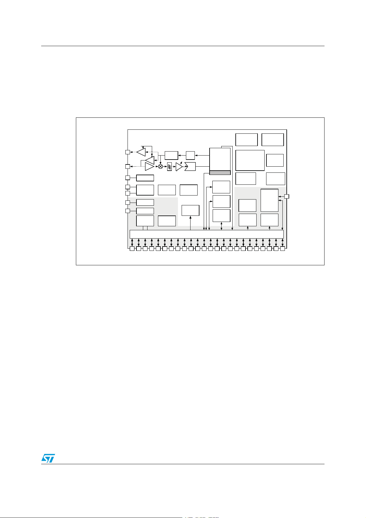
STM32W108C8 Description
Packet sniffer
ADC
RF_P,N
Program
Flash
64 kBytes
Data
SRAM
8 kBytes
HF crystal
OSC
LF crystal
OSC
General
Purpose
ADC
Serial
Wire and
JTAG
debug
Internal LF
RC-OSC
GPIO multiplexor swtich
Chip
manager
Regulator
Bias
2ndlevel
Interrupt
controller
RF_TX_ALT_P,N
OSCA
OSCB
PA[7:0], PB[7:0], PC[7:0]
Encryption
acclerat or
IF
Always
Powered
Domain
ARM CORTEX-M3
®
CPU with NVIC
and MPU
VREG_OUT
Watchdog
PA se lect
LNA
PA
PA
DAC
MAC
+
Baseband
Sleep
timer
BIAS_R
POR
nRESET
General
purpose
timers
GPIO
regist ers
UART/
SPI/I
2
C
SYNTH
Inter nal H F
RC-OSC
TX_ACTIVE
SWCLK,
JTCK
Calibration
ADC
Packet Trace
CPU debug
TPIU/ITM/
FPB/DWT
-36
1 Description
The STM32W108C8 is a fully integrated System-on-Chip that integrates a 2.4 GHz, IEEE
802.15.4-compliant transceiver, 32-bit ARM® Cortex™-M3 microprocessor, Flash and RAM
memory, and peripherals of use to designers of 802.15.4-based systems.
Figure 1. STM32W108C8 block diagram
The transceiver utilizes an efficient architecture that exceeds the dynamic range
requirements imposed by the IEEE 802.15.4-2003 standard by over 15 dB. The integrated
receive channel filtering allows for robust co-existence with other communication standards
in the 2.4 GHz spectrum, such as IEEE 802.11 and Bluetooth. The integrated regulator,
VCO, loop filter, and power amplifier keep the external component count low. An optional
high performance radio mode (boost mode) is software-selectable to boost dynamic range.
The integrated 32-bit ARM® Cortex™-M3 microprocessor is highly optimized for high
performance, low power consumption, and efficient memory utilization. Including an
integrated MPU, it supports two different modes of operation: Privileged mode and
Unprivileged mode. This architecture could be used to separate the networking stack from
the application code and prevent unwanted modification of restricted areas of memory and
registers resulting in increased stability and reliability of deployed solutions.
The STM32W108C8 has 64 Kbytes of embedded Flash memory and 8 Kbytes of integrated
RAM for data and program storage. The STM32W108C8 HAL software employs an effective
wear-leveling algorithm that optimizes the lifetime of the embedded Flash.
To maintain the strict timing requirements imposed by the IEEE 802.15.4-2003 standards,
the STM32W108C8 integrates a number of MAC functions into the hardware. The MAC
hardware handles automatic ACK transmission and reception, automatic backoff delay, and
clear channel assessment for transmission, as well as automatic filtering of received
packets. A packet trace interface is also integrated with the MAC, allowing complete, nonintrusive capture of all packets to and from the STM32W108C8.
Doc ID 018587 Rev 2 10/215
Page 12

Description STM32W108C8
The STM32W108C8 offers a number of advanced power management features that enable
long battery life. A high-frequency internal RC oscillator allows the processor core to begin
code execution quickly upon waking. Various deep sleep modes are available with less than
1 µA power consumption while retaining RAM contents. To support user-defined
applications, on-chip peripherals include UART, SPI, I
as well as up to 24 GPIOs. Additionally, an integrated voltage regulator, power-on-reset
circuit, and sleep timer are available.
2
C, ADC and general-purpose timers,
1.1 Development tools
The STM32W108C8 implements both the ARM Serial Wire and JTAG debug interfaces.
These interfaces provide real time, non-intrusive programming and debugging capabilities.
Serial Wire and JTAG provide the same functionality, but are mutually exclusive. The Serial
Wire interface uses two pins; the JTAG interface uses five. Serial Wire is preferred, since it
uses fewer pins.
The STM32W108C8 also integrates the standard ARM system debug components: Flash
Patch and Breakpoint (FPB), Data Watchpoint and Trace (DWT), and Instrumentation Trace
Macrocell (DWT).
11/215 Doc ID 018587 Rev 2
Page 13

STM32W108C8 Description
1.2 Overview
1.2.1 Functional description
The STM32W108C8 radio receiver is a low-IF, super-heterodyne receiver. The architecture
has been chosen to optimize co-existence with other devices in the 2.4 GHz band (namely,
WIFI and Bluetooth), and to minimize power consumption. The receiver uses differential
signal paths to reduce sensitivity to noise interference. Following RF amplification, the signal
is downconverted by an image-rejecting mixer, filtered, and then digitized by an ADC.
The radio transmitter uses an efficient architecture in which the data stream directly
modulates the VCO frequency. An integrated power amplifier (PA) provides the output
power. Digital logic controls Tx path and output power calibration. If the STM32W108C8 is to
be used with an external PA, use the TX_ACTIVE or nTX_ACTIVE signal to control the
timing of the external switching logic.
The integrated 4.8 GHz VCO and loop filter minimize off-chip circuitry. Only a 24 MHz
crystal with its loading capacitors is required to establish the PLL local oscillator signal.
The MAC interfaces the on-chip RAM to the Rx and Tx baseband modules. The MAC
provides hardware-based IEEE 802.15.4 packet-level filtering. It supplies an accurate
symbol time base that minimizes the synchronization effort of the software stack and meets
the protocol timing requirements. In addition, it provides timer and synchronization
assistance for the IEEE 802.15.4 CSMA-CA algorithm.
The STM32W108C8 integrates an ARM® Cortex-M3 microprocessor, revision r1p1. This
industry-leading core provides 32 bit performance and is very power efficient. It has
excellent code density using the ARM® Thumb 2 instruction set. The processor can be
operated at 12 MHz or 24 MHz when using the crystal oscillator, or at 6 MHz or 12 MHz
when using the integrated high frequency RC oscillator.
The STM32W108C8 has 64 Kbytes of Flash memory, 8 Kbytes of SRAM on-chip, and the
ARM configurable memory protection unit (MPU).
The STM32W108C8 contains 24 GPIO pins shared with other peripheral or alternate
functions. Because of flexible routing within the STM32W108C8, external devices can use
the alternate functions on a variety of different GPIOs. The integrated Serial Controller SC1
can be configured for SPI (master or slave), I
Serial Controller SC2 can be configured for SPI (master or slave) or I
operation.
The STM32W108C8 has a general purpose ADC which can sample analog signals from six
GPIO pins in single-ended or differential modes. It can also sample the regulated supply
VDD_PADSA, the voltage reference VREF, and GND. The ADC has two selectable voltage
ranges: 0 V to 1.2 V (normal) and 0.1 V to 0.1 V below the high voltage supply (high). The
ADC has a DMA mode to capture samples and automatically transfer them into RAM. The
integrated voltage reference for the ADC, VREF, can be made available to external circuitry.
An external voltage reference can also be driven into the ADC.
The STM32W108C8 contains four oscillators: a high frequency 24 MHz external crystal
oscillator, a high frequency 12 MHz internal RC oscillator, an optional low frequency 32.768
kHz external crystal oscillator, and a 10 kHz internal RC oscillator.
2
C (master-only), or UART operation, and the
2
C (master-only)
The STM32W108C8 has an ultra low power, deep sleep state with a choice of clocking
modes. The sleep timer can be clocked with either the external 32.768 kHz crystal oscillator
or with a 1 kHz clock derived from the internal 10 kHz RC oscillator. Alternatively, all clocks
Doc ID 018587 Rev 2 12/215
Page 14

Description STM32W108C8
can be disabled for the lowest power mode. In the lowest power mode, only external events
on GPIO pins will wake up the chip. The STM32W108C8 has a fast startup time (typically
100 µs) from deep sleep to the execution of the first ARM® Cortex-M3 instruction.
The STM32W108C8 contains three power domains. The always-on high voltage supply
powers the GPIO pads and critical chip functions. Regulated low voltage supplies power the
rest of the chip. The low voltage supplies are be disabled during deep sleep to reduce power
consumption. Integrated voltage regulators generate regulated 1.25 V and 1.8 V voltages
from an unregulated supply voltage. The 1.8 V regulator output is decoupled and routed
externally to supply analog blocks, RAM, and Flash memories. The 1.25 V regulator output
is decoupled externally and supplies the core logic.
The digital section of the receiver uses a coherent demodulator to generate symbols for the
hardware-based MAC. The digital receiver also contains the analog radio calibration
routines and controls the gain within the receiver path.
In addition to 2 general-purpose timers, the STM32W108C8 also contains a watchdog timer
to ensure protection against software crashes and CPU lockup, a 32-bit sleep timer
dedicated to system timing and waking from sleep at specific times and an ARM® standard
system event timer in the NVIC.
The STM32W108C8 integrates hardware support for a Packet Trace module, which allows
robust packet-based debug.
Note: The STM32W108C8 is not pin-compatible with the previous generation chip, the SN250,
except for the RF section of the chip. Pins 1-11 and 45-48 are compatible, to ease migration
to the STM32W108C8.
1.2.2 ARM® Cortex™-M3 core
The STM32W108C8 integrates the ARM® Cortex™-M3 microprocessor, revision r1p1,
developed by ARM Ltd, making the STM32W108C8 a true system-on-a-chip solution. The
ARM® Cortex-M3 is an advanced 32-bit modified Harvard architecture processor that has
separate internal program and data buses, but presents a unified program and data address
space to software. The word width is 32 bits for both the program and data sides. The
ARM® Cortex-M3 allows unaligned word and half-word data accesses to support efficientlypacked data structures.
The ARM® Cortex-M3 clock speed is configurable to 6 MHz, 12 MHz, or 24 MHz. For
normal operation 12 MHz is preferred over 24 MHz due to its lower power consumption. The
6 MHz operation can only be used when radio operations are not required since the radio
requires an accurate 12 MHz clock.
The ARM® Cortex-M3 in the STM32W108C8 has also been enhanced to support two
separate memory protection levels. Basic protection is available without using the MPU, but
the usual operation uses the MPU. The MPU protects unimplemented areas of the memory
map to prevent common software bugs from interfering with software operation. The
architecture could also separate the networking stack from the application code using a fine
granularity RAM protection module. Errant writes are captured and details are reported to
the developer to assist in tracking down and fixing issues.
13/215 Doc ID 018587 Rev 2
Page 15

STM32W108C8 Documentation conventions
2 Documentation conventions
Table 1. Description of abbreviations used for bitfield access
Abbreviation Description
Read/Write (rw) Software can read and write to these bits.
Read-only (r) Software can only read these bits.
Write only (w) Software can only write to this bit. Reading returns the reset value.
Read/Write in (MPU)
Privileged mode only (rws)
1. The conditions under which the hardware (core) sets or clears this field are explained in details in the
bitfield description, as well as the events that may be generated by writing to the bit.
Software can read and write to these bits only in Privileged mode. For
more information, please refer to RAM memory protection on page 28
and Memory protection unit on page 28.
(1)
Doc ID 018587 Rev 2 14/215
Page 16
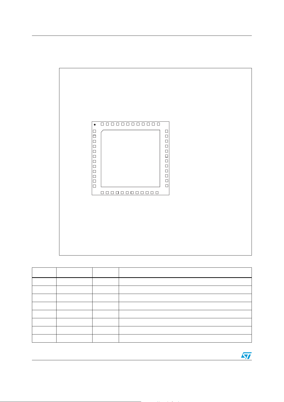
Pinout and pin description STM32W108C8
Ai15261
Ground pad on back
VDD_24MHZ
RF_P
RF_N
VDD_RF
RF_TX_ALT_P
RF_TX_ALT_N
VDD_IF
BIAS_R
VDD_PADSA
PC5, TX_ACTIVE
VDD_PADS
PA1, TIM2C3, SC2SDA, SC2MISO
PA0, TIM2C1, SC2MOSI
PA7, TIM1C4, REG_EN
VDD_CORE
VREG_OUT
PC6, OSC32B, nTX_ACTIVE
VDD_PADS
PA2, TIM2C4, SC2SCL, SC2SCLK
PB0, VREF, IRQA, TRACECLK, TIM1CLK, TIM2MSK
PC4, JTMS, SWDIO
PC3, JTDI
PC2, JTDO, SWO
SWCLK, JTCK
VDD_PADS
PA5, ADC5, PTI_DATA, nBOOTMODE, TRACEDATA3
PA4, ADC4, PTI_EN, TRACEDATA2
PA 3, SC2nSSEL, TRACECLK, TIM2C2
PC1, ADC3, SWO, TRACEDATA0
VDD_MEM
PB7, ADC2, IRQC, TIM1C2
PB5, ADC0, TIM2CLK, TIM1MSK
VDD_CORE
VDD_PRE
OSCA
PC0, JRST, IRQDn, TRACEDATA1
OSCB
VDD_PADS
1
2
3
4
5
6
7
8
9
10
11
12
13 14 15 16 17 18 19 20 21 22
23 24
36
35
34
33
32
31
30
29
28
27
26
25
48 47 46 45 44 43 42 41 40 39
38 37
VDD_VCO
nRESET
PC7, OSC32A, OSC32_EXT
PB3, TIM2C3, SC1nCTS, SC1SCLK
PB4, TIM2C4, SC1nRTS, SC1nSSEL
PB1, SC1MISO, SC1MOSI, SC1SDA , SC1TXD, TIM2C1
PA6, TIM1C3
PB2, SC1MISO, SC1MOSI, SC1SCL, SC1RXD, TIM2C2
VDD_SYNTH
PB6, ADC1, IRQ6, TIM1C1
3 Pinout and pin description
Figure 2. 48-pin VFQFPN pinout
Table 2. Pin descriptions
Pin no. Signal Direction Description
1 VDD_24MHZ Power 1.8V high-frequency oscillator supply
2 VDD_VCO Power 1.8V VCO supply
3 RF_P I/O Differential (with RF_N) receiver input/transmitter output
4 RF_N I/O Differential (with RF_P) receiver input/transmitter output
5 VDD_RF Power 1.8V RF supply (LNA and PA)
6 RF_TX_ALT_P O Differential (with RF_TX_ALT_N) transmitter output (optional)
7 RF_TX_ALT_N O Differential (with RF_TX_ALT_P) transmitter output (optional)
8 VDD_IF Power 1.8V IF supply (mixers and filters)
15/215 Doc ID 018587 Rev 2
Page 17

STM32W108C8 Pinout and pin description
Table 2. Pin descriptions (continued)
Pin no. Signal Direction Description
9 BIAS_R I Bias setting resistor
10 VDD_PADSA Power Analog pad supply (1.8V)
PC5 I/O Digital I/O
11
12 nRESET I Active low chip reset (internal pull-up)
13
14
TX_ACTIVE O
PC6 I/O Digital I/O
OSC32B I/O
nTX_ACTIVE O
PC7 I/O Digital I/O
OSC32A I/O
Logic-level control for external Rx/Tx switch. The STM32W108C8
baseband controls TX_ACTIVE and drives it high (VDD_PADS)
when in Tx mode.
Select alternate output function with GPIO_PCCFGH[7:4]
32.768 kHz crystal oscillator
Select analog function with GPIO_PCCFGH[11:8]
Inverted TX_ACTIVE signal (see PC5)
Select alternate output function with GPIO_PCCFGH[11:8]
32.768 kHz crystal oscillator.
Select analog function with GPIO_PCCFGH[15:12]
OSC32_EXT I Digital 32 kHz clock input source
15 VREG_OUT Power Regulator output (1.8 V while awake, 0 V during deep sleep)
16 VDD_PADS Power Pads supply (2.1-3.6 V)
17 VDD_CORE Power 1.25 V digital core supply decoupling
18
PA 7
TIM1_CH4
REG_EN O External regulator open drain output. (Enabled after reset.)
I/O
High current
O
I Timer 1 Channel 4 input. (Cannot be remapped.)
Digital I/O. Disable REG_EN with GPIO_DBGCFG[4]
Timer 1 Channel 4 output
Enable timer output with TIM1_CCER
Select alternate output function with GPIO_PACFGH[15:12]
Disable REG_EN with GPIO_DBGCFG[4]
Doc ID 018587 Rev 2 16/215
Page 18

Pinout and pin description STM32W108C8
Table 2. Pin descriptions (continued)
Pin no. Signal Direction Description
PB3 I/O Digital I/O
Timer 2 channel 3 output
Enable remap with TIM2_OR[6]
Enable timer output in TIM2_CCER
Select alternate output function with GPIO_PBCFGL[15:12]
UART CTS handshake of Serial Controller 1
Enable with SC1_UARTCFG[5]
Select UART with SC1_MODE
SPI master clock of Serial Controller 1
Either disable timer output in TIM2_CCER or disable remap with
TIM2_OR[6]
Enable master with SC1_SPICFG[4]
Select SPI with SC1_MODE
Select alternate output function with GPIO_PBCFGL[15:12]
SPI slave clock of Serial Controller 1
Enable slave with SC1_SPICFG[4]
Select SPI with SC1_MODE
Timer 2 channel 4 output
Enable remap with TIM2_OR[7]
Enable timer output in TIM2_CCER
Select alternate output function with GPIO_PBCFGH[3:0]
19
TIM2_CH3
(see Pin 22)
UART_CTS I
SC1SCLK
PB4 I/O Digital I/O
TIM2_CH4
(see also Pin 24)
O
I Timer 2 channel 3 input. Enable remap with TIM2_OR[6].
O
I
O
20
UART_RTS O
SC1nSSEL I
I Timer 2 channel 4 input. Enable remap with TIM2_OR[7].
UART RTS handshake of Serial Controller 1
Either disable timer output in TIM2_CCER or disable remap with
TIM2_OR[7]
Enable with SC1_UARTCFG[5]
Select UART with SC1_MODE
Select alternate output function with GPIO_PBCFGH[3:0]
SPI slave select of Serial Controller 1
Enable slave with SC1_SPICFG[4]
Select SPI with SC1_MODE
17/215 Doc ID 018587 Rev 2
Page 19

STM32W108C8 Pinout and pin description
Table 2. Pin descriptions (continued)
Pin no. Signal Direction Description
PA0 I/O Digital I/O
Timer 2 channel 1 output
TIM2_CH1
O
(see also Pin 30)
I Timer 2 channel 1 input. Disable remap with TIM2_OR[4].
21
O
SC2MOSI
I
PA1 I/O Digital I/O
TIM2_CH3
O
(see also Pin 19)
I Timer 2 channel 3 input. Disable remap with TIM2_OR[6].
SC2SDA I/O
22
O
SC2MISO
I
23 VDD_PADS Power Pads supply (2.1-3.6V)
Disable remap with TIM2_OR[4]
Enable timer output in TIM2_CCER
Select alternate output function with GPIO_PACFGL[3:0]
SPI master data out of Serial Controller 2
Either disable timer output in TIM2_CCER or enable remap with
TIM2_OR[4]
Enable master with SC2_SPICFG[4]
Select SPI with SC2_MODE
Select alternate output function with GPIO_PACFGL[3:0]
SPI slave data in of Serial Controller 2
Enable slave with SC2_SPICFG[4]
Select SPI with SC2_MODE
Timer 2 channel 3 output
Disable remap with TIM2_OR[6]
Enable timer output in TIM2_CCER
Select alternate output function with GPIO_PACFGL[7:4]
2
I
C data of Serial Controller 2
Either disable timer output in TIM2_CCER or enable remap with
TIM2_OR[6]
Select I
2
C with SC2_MODE
Select alternate open-drain output function with GPIO_PACFGL[7:4]
SPI slave data out of Serial Controller 2
Either disable timer output in TIM2_CCER or enable remap with
TIM2_OR[6]
Enable slave with SC2_SPICFG[4]
Select SPI with SC2_MODE
Select alternate output function with GPIO_PACFGL[7:4]
SPI master data in of Serial Controller 2
Enable slave with SC2_SPICFG[4]
Select SPI with SC2_MODE
Doc ID 018587 Rev 2 18/215
Page 20

Pinout and pin description STM32W108C8
Table 2. Pin descriptions (continued)
Pin no. Signal Direction Description
PA2 I/O Digital I/O
Timer 2 channel 4 output
Disable remap with TIM2_OR[7]
Enable timer output in TIM2_CCER
Select alternate output function with GPIO_PACFGL[11:8]
2
I
C clock of Serial Controller 2
Either disable timer output in TIM2_CCER or enable remap with
TIM2_OR[7]
Select I
2
C with SC2_MODE
Select alternate open-drain output function with
GPIO_PACFGL[11:8]
SPI master clock of Serial Controller 2
Either disable timer output in TIM2_CCER or enable remap with
TIM2_OR[7]
Enable master with SC2_SPICFG[4]
Select SPI with SC2_MODE
Select alternate output function with GPIO_PACFGL[11:8]
SPI slave clock of Serial Controller 2
Enable slave with SC2_SPICFG[4]
Select SPI with SC2_MODE
24
TIM2_CH4
O
(see also Pin 20)
SC2SCL I/O
O
SC2SCLK
I Timer 2 channel 4 input. Disable remap with TIM2_OR[7].
I
25
PA3 I/O Digital I/O
SPI slave select of Serial Controller 2
SC2nSSEL I
Enable slave with SC2_SPICFG[4]
Select SPI with SC2_MODE
Synchronous CPU trace clock
TRACECLK
(see also Pin 36)
O
Either disable timer output in TIM2_CCER or enable remap with
TIM2_OR[5]
Enable trace interface in ARM core
Select alternate output function with GPIO_PACFGL[15:12]
Timer 2 channel 2 output
TIM2_CH2
(see also Pin 31)
O
Disable remap with TIM2_OR[5]
Enable timer output in TIM2_CCER
Select alternate output function with GPIO_PACFGL[15:12]
I Timer 2 channel 2 input. Disable remap with TIM2_OR[5].
19/215 Doc ID 018587 Rev 2
Page 21

STM32W108C8 Pinout and pin description
Table 2. Pin descriptions (continued)
Pin no. Signal Direction Description
PA4 I/O Digital I/O
ADC4 Analog ADC Input 4. Select analog function with GPIO_PACFGH[3:0].
Frame signal of Packet Trace Interface (PTI).
26
PTI_EN O
TRACEDATA2 O
PA5 I/O Digital I/O
ADC5 Analog ADC Input 5. Select analog function with GPIO_PACFGH[7:4].
PTI_DATA O
27
nBOOTMODE I
Disable trace interface in ARM core.
Select alternate output function with GPIO_PACFGH[3:0].
Synchronous CPU trace data bit 2.
Select 4-wire synchronous trace interface in ARM core.
Enable trace interface in ARM core.
Select alternate output function with GPIO_PACFGH[3:0].
Data signal of Packet Trace Interface (PTI).
Disable trace interface in ARM core.
Select alternate output function with GPIO_PACFGH[7:4].
Embedded serial bootloader activation out of reset.
Signal is active during and immediately after a reset on NRST. See
Section 6.2: Resets on page 34 for details.
Synchronous CPU trace data bit 3.
TRACEDATA3 O
28 VDD_PADS Power Pads supply (2.1-3.6 V)
PA 6
29
TIM1_CH3
I/O
High current
O
I Timer 1 channel 3 input (Cannot be remapped.)
Select 4-wire synchronous trace interface in ARM core.
Enable trace interface in ARM core.
Select alternate output function with GPIO_PACFGH[7:4]
Digital I/O
Timer 1 channel 3 output
Enable timer output in TIM1_CCER
Select alternate output function with GPIO_PACFGH[11:8]
Doc ID 018587 Rev 2 20/215
Page 22

Pinout and pin description STM32W108C8
Table 2. Pin descriptions (continued)
Pin no. Signal Direction Description
PB1 I/O Digital I/O
SPI slave data out of Serial Controller 1
Either disable timer output in TIM2_CCER or disable remap with
SC1MISO O
SC1MOSI O
30
SC1SDA I/O
SC1TXD O
TIM2_OR[4]
Select SPI with SC1_MODE
Select slave with SC1_SPICR
Select alternate output function with GPIO_PBCFGL[7:4]
SPI master data out of Serial Controller 1
Either disable timer output in TIM2_CCER or disable remap with
TIM2_OR[4]
Select SPI with SC1_MODE
Select master with SC1_SPICR
Select alternate output function with GPIO_PBCFGL[7:4]
2
I
C data of Serial Controller 1
Either disable timer output in TIM2_CCER,
or disable remap with TIM2_OR[4]
Select I
2
C with SC1_MODE
Select alternate open-drain output function with GPIO_PBCFGL[7:4]
UART transmit data of Serial Controller 1
Either disable timer output in TIM2_CCER or disable remap with
TIM2_OR[4]
Select UART with SC1_MODE
Select alternate output function with GPIO_PBCFGL[7:4]
TIM2_CH1
(see also Pin 21)
Timer 2 channel 1 output
O
Enable remap with TIM2_OR[4]
Enable timer output in TIM2_CCER
Select alternate output function with GPIO_PACFGL[7:4]
I Timer 2 channel 1 input. Disable remap with TIM2_OR[4].
21/215 Doc ID 018587 Rev 2
Page 23

STM32W108C8 Pinout and pin description
Table 2. Pin descriptions (continued)
Pin no. Signal Direction Description
PB2 I/O Digital I/O
SPI master data in of Serial Controller 1
31
SC1MISO I
SC1MOSI I
SC1SCL I/O
Select SPI with SC1_MODE
Select master with SC1_SPICR
SPI slave data in of Serial Controller 1
Select SPI with SC1_MODE
Select slave with SC1_SPICR
2
I
C clock of Serial Controller 1
Either disable timer output in TIM2_CCER,
or disable remap with TIM2_OR[5]
Select I
2
C with SC1_MODE
Select alternate open-drain output function with
GPIO_PBCFGL[11:8]
32
33
34
SC1RXD I
TIM2_CH2
O
(see also Pin 25)
SWCLK I/O
JTCK I
PC2 I/O
JTDO O
SWO O
PC3 I/O
JTDI I
UART receive data of Serial Controller 1
Select UART with SC1_MODE
Timer 2 channel 2 output
Enable remap with TIM2_OR[5]
Enable timer output in TIM2_CCER
Select alternate output function with GPIO_PBCFGL[11:8]
I Timer 2 channel 2 input. Enable remap with TIM2_OR[5].
Serial Wire clock input/output with debugger
Selected when in Serial Wire mode (see JTMS description, Pin 35)
JTAG clock input from debugger
Selected when in JTAG mode (default mode, see JTMS description,
Pin 35)
Internal pull-down is enabled
Digital I/O
Enable with GPIO_DBGCFG[5]
JTAG data out to debugger
Selected when in JTAG mode (default mode, see JTMS description,
Pin 35)
Serial Wire Output asynchronous trace output to debugger
Select asynchronous trace interface in ARM core
Enable trace interface in ARM core
Select alternate output function with GPIO_PCCFGL[11:8]
Enable Serial Wire mode (see JTMS description, Pin 35)
Internal pull-up is enabled
Digital I/O
Either Enable with GPIO_DBGCFG[5],
or enable Serial Wire mode (see JTMS description)
JTAG data in from debugger
Selected when in JTAG mode (default mode, see JTMS description,
Pin 35)
Internal pull-up is enabled
Doc ID 018587 Rev 2 22/215
Page 24

Pinout and pin description STM32W108C8
Table 2. Pin descriptions (continued)
Pin no. Signal Direction Description
35
36
PC4 I/O
JTMS I
SWDIO I/O
PB0 I/O Digital I/O
VREF Analog O
VREF Analog I
IRQA I External interrupt source A.
TRACECLK
(see also Pin 25)
TIM1CLK I Timer 1 external clock input.
TIM2MSK I Timer 2 external clock mask input.
O
Digital I/O
Enable with GPIO_DBGCFG[5]
JTAG mode select from debugger
Selected when in JTAG mode (default mode)
JTAG mode is enabled after power-up or by forcing NRST low
Select Serial Wire mode using the ARM-defined protocol through a
debugger
Internal pull-up is enabled
Serial Wire bidirectional data to/from debugger
Enable Serial Wire mode (see JTMS description)
Select Serial Wire mode using the ARM-defined protocol through a
debugger
Internal pull-up is enabled
ADC reference output.
Enable analog function with GPIO_PBCFGL[3:0].
ADC reference input.
Enable analog function with GPIO_PBCFGL[3:0].
Enable reference output with an ST system function.
Synchronous CPU trace clock.
Enable trace interface in ARM core.
Select alternate output function with GPIO_PBCFGL[3:0].
37 VDD_PADS Power Pads supply (2.1 to 3.6 V).
PC1 I/O Digital I/O
ADC3 Analog
38
39 VDD_MEM Power 1.8 V supply (flash, RAM)
23/215 Doc ID 018587 Rev 2
SWO
(see also Pin 33)
TRACEDATA0 O
O
ADC Input 3
Enable analog function with GPIO_PCCFGL[7:4]
Serial Wire Output asynchronous trace output to debugger
Select asynchronous trace interface in ARM core
Enable trace interface in ARM core
Select alternate output function with GPIO_PCCFGL[7:4]
Synchronous CPU trace data bit 0
Select 1-, 2- or 4-wire synchronous trace interface in ARM core
Enable trace interface in ARM core
Select alternate output function with GPIO_PCCFGL[7:4]
Page 25

STM32W108C8 Pinout and pin description
Table 2. Pin descriptions (continued)
Pin no. Signal Direction Description
Digital I/O
40
PC0
I/O
High current
JRST I
(1)
IRQD
TRACEDATA1 O
I Default external interrupt source D
Either enable with GPIO_DBGCFG[5],
or enable Serial Wire mode (see JTMS description, Pin 35) and
disable TRACEDATA1
JTAG reset input from debugger
Selected when in JTAG mode (default mode, see JTMS description)
and TRACEDATA1 is disabled
Internal pull-up is enabled
Synchronous CPU trace data bit 1
Select 2- or 4-wire synchronous trace interface in ARM core
Enable trace interface in ARM core
Select alternate output function with GPIO_PCCFGL[3:0]
41
42
43
PB7
I/O
High current
ADC2 Analog
(1)
IRQC
I Default external interrupt source C
Digital I/O
ADC Input 2
Enable analog function with GPIO_PBCFGH[15:12]
Timer 1 channel 2 output
TIM1_CH2
O
Enable timer output in TIM1_CCER
Select alternate output function with GPIO_PBCFGH[15:12]
I Timer 1 channel 2 input (Cannot be remapped)
PB6
I/O
High current
ADC1 Analog
Digital I/O
ADC Input 1
Enable analog function with GPIO_PBCFGH[11:8]
IRQB I External interrupt source B
Timer 1 channel 1 output
TIM1_CH1
O
Enable timer output in TIM1_CCER
Select alternate output function with GPIO_PBCFGH[11:8]
I Timer 1 channel 1 input (Cannot be remapped)
PB5 I/O Digital I/O
ADC0 Analog
ADC Input 0
Enable analog function with GPIO_PBCFGH[7:4]
TIM2CLK I Timer 2 external clock input
TIM1MSK I Timer 2 external clock mask input
44 VDD_CORE Power 1.25 V digital core supply decoupling
45 VDD_PRE Power 1.8 V prescaler supply
46 VDD_SYNTH Power 1.8 V synthesizer supply
47 OSCB I/O
24 MHz crystal oscillator or left open when using external clock input
on OSCA
Doc ID 018587 Rev 2 24/215
Page 26

Pinout and pin description STM32W108C8
Table 2. Pin descriptions (continued)
Pin no. Signal Direction Description
48 OSCA I/O 24 MHz crystal oscillator or external clock input
49 GND Ground Ground supply pad in the bottom center of the package.
1. IRQC and IRQD external interrupts can be mapped to any digital I/O pin using the using the GPIO_IRQCSEL and
GPIO_IRQDSEL registers.
25/215 Doc ID 018587 Rev 2
Page 27
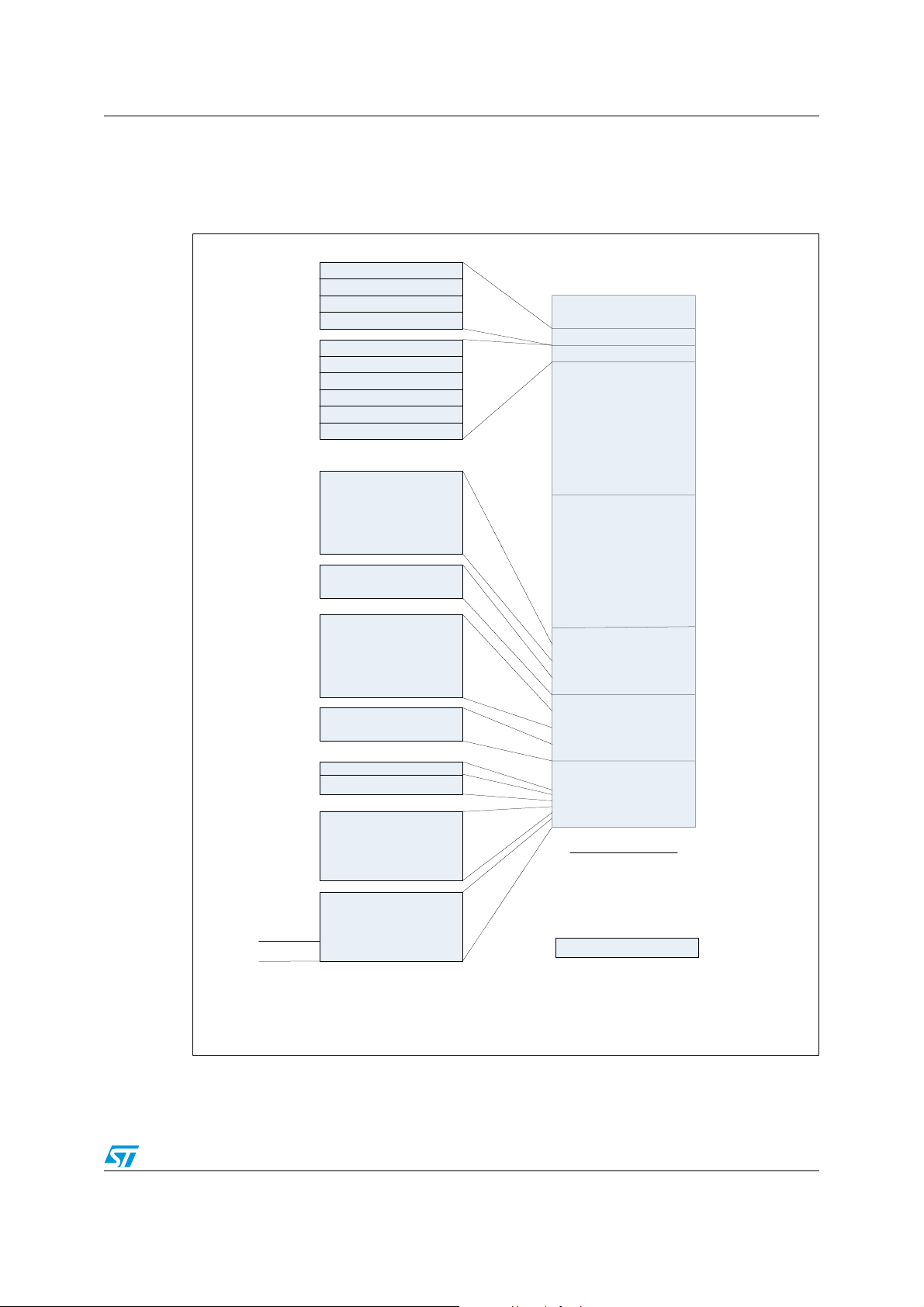
STM32W108C8 Embedded memory
-AIN&LASH"LOCK
,OWERMAPPING
.ORMAL-ODE
X
X&&&&
2!-K"
MAPPEDONTO3YSTEM
INTERFACE
X
X&&&
2!-BITBAND
ALIASREGION
MAPPEDONTO3YSTEM
INTERFACE
NOTUSED
X
X
&LASH
2!-
0ER IP HER AL
2EGISTERS
MAPPEDONTO3YSTEM
INTERFACE
2EGISTERBITBAND
ALIASREGION
MAPPEDONTO3YSTEM
INTERFACE
NOTUSED
X
X888
X
X888
.OTUSED
0RIVATEPERIPHBUSINTERNAL
.OTUSED
0RIVATEPERIPHBUSEXTERNAL
.OTUSED
.OTUSED
.OTUSED
X%
)4-
$74
&0"
.6)#
40)5
2/-TABLE
X%
X%
X%
X%%
X%&
X%&&&&
X%
X%
X%
X%&&
X%&&&&&
X%
X
X
X
X
X!
X&&&&&&&&
X$&&&&&&&
X&&&&&&&
X&&&&&&&
X&&&&&&&
X&&&&&&&
&IXED)NFO"LOCKK"
#USTOMER)NFO"LOCKK"
X
X&&
X&&
X
-AIN&LASH"LOCKK"
5PPERMAPPING
"OOTMODE
X
X&&&&
&IXED)NFO"LOCKK"
/PTIONALBOOT MODE
MAPS &IXED)NFO"LOCK
TO THESTARTOFMEMORY
X&&
.OTUSED
.OTUSED
K"
-36
4 Embedded memory
Figure 3. STM32W108C8 memory mapping
Doc ID 018587 Rev 2 26/215
Page 28

Embedded memory STM32W108C8
4.1 Flash memory
The STM32W108C8 provides a total of 66.5 Kbytes of Flash memory in three separate
blocks:
● Main Flash Block (MFB)
● Fixed Information Block (FIB)
● Customer Information Block (CIB)
The MFB is divided into 641024-byte pages. The CIB is a single 512-byte page. The FIB is a
single 2048-byte page. The smallest erasable unit is one page and the smallest writable unit
is an aligned 16-bit half-word. The flash is rated to have a guaranteed 1,000 write/erase
cycles. The flash cell has been qualified for a data retention time of >100 years at room
temperature.
Flash may be programmed either through the Serial Wire/JTAG interface or through
bootloader software. Programming flash through Serial Wire/JTAG requires the assistance
of RAM-based utility code. Programming through a bootloader requires specific software for
over-the-air loading or serial link loading. A simplified, serial-link-only bootloader is also
available preprogrammed into the FIB.
4.2 Random-access memory
The STM32W108C8 has 8 Kbytes of static RAM on-chip. The start of RAM is mapped to
address 0x20000000. Although the ARM® Cortex-M3 allows bit band accesses to this
address region, the standard MPU configuration does not permit use of the bit-band feature.
The RAM is physically connected to the AHB System bus and is therefore accessible to both
the ARM® Cortex-M3 microprocessor and the debugger. The RAM can be accessed for
both instruction and data fetches as bytes, half words, or words. The standard MPU
configuration does not permit execution from the RAM, but for special purposes, such as
programming the main flash block, the MPU may be disabled. To the bus, the RAM appears
as 32-bit wide memory and in most situations has zero wait state read or write access. In
the higher CPU clock mode the RAM requires two wait states. This is handled by hardware
transparent to the user application with no configuration required.
4.2.1 Direct memory access (DMA) to RAM
Several of the peripherals are equipped with DMA controllers allowing them to transfer data
into and out of RAM autonomously. This applies to the radio (802.15.4 MAC), general
purpose ADC, and both serial controllers. In the case of the serial controllers, the DMA is full
duplex so that a read and a write to RAM may be requested at the same time. Thus there
are six DMA channels in total.
The STM32W108C8 integrates a DMA arbiter that ensures fair access to the
microprocessor as well as the peripherals through a fixed priority scheme appropriate to the
memory bandwidth requirements of each master. The priority scheme is as follows, with the
top peripheral being the highest priority:
1. General Purpose ADC
2. Serial Controller 2 Receive
3. Serial Controller 2 Transmit
4. MAC
5. Serial Controller 1 Receive
27/215 Doc ID 018587 Rev 2
Page 29

STM32W108C8 Embedded memory
6. Serial Controller 1 Transmit
4.2.2 RAM memory protection
The STM32W108C8 integrates two memory protection mechanisms. The first memory
protection mechanism is through the ARM® Cortex-M3 Memory Protection Unit (MPU)
described in the Memory Protection Unit section. The MPU may be used to protect any area
of memory. MPU configuration is normally handled by software. The second memory
protection mechanism is through a fine granularity RAM protection module. This allows
segmentation of the RAM into 32-byte blocks where any block can be marked as write
protected. An attempt to write to a protected RAM block using a user mode write results in a
bus error being signaled on the AHB System bus. A system mode write is allowed at any
time and reads are allowed in either mode. The main purpose of this fine granularity RAM
protection module is to notify the stack of erroneous writes to system areas of memory. RAM
protection is configured using a group of registers that provide a bit map. Each bit in the map
represents a 32-byte block of RAM. When the bit is set the block is write protected.
The fine granularity RAM memory protection mechanism is also available to the peripheral
DMA controllers. A register bit is provided to enable the memory protection to include DMA
writes to protected memory. If a DMA write is made to a protected location in RAM, a
management interrupt is generated. At the same time the faulting address and the
identification of the peripheral is captured for later debugging. Note that only peripherals
capable of writing data to RAM, such as received packet data or a received serial port
character, can generate this interrupt.
4.3 Memory protection unit
The STM32W108C8 includes the ARM® Cortex-M3 Memory Protection Unit, or MPU. The
MPU controls access rights and characteristics of up to eight address regions, each of
which may be divided into eight equal sub-regions. Refer to the ARM® Cortex-M3 Technical
Reference Manual (DDI 0337A) for a detailed description of the MPU.
ST software configures the MPU in a standard configuration and application software should
not modify it. The configuration is designed for optimal detection of illegal instruction or data
accesses. If an illegal access is attempted, the MPU captures information about the access
type, the address being accessed, and the location of the offending software. This simplifies
software debugging and increases the reliability of deployed devices. As a consequence of
this MPU configuration, accessing RAM and register bit-band address alias regions is not
permitted, and generates a bus fault if attempted.
Doc ID 018587 Rev 2 28/215
Page 30

Radio frequency module STM32W108C8
5 Radio frequency module
The radio module consists of an analog front end and digital baseband as shown in
Figure 1: STM32W108C8 block diagram.
5.1 Receive (Rx) path
The Rx path uses a low-IF, super-heterodyne receiver that rejects the image frequency
using complex mixing and polyphase filtering. In the analog domain, the input RF signal
from the antenna is first amplified and mixed down to a 4 MHz IF frequency. The mixers'
output is filtered, combined, and amplified before being sampled by a 12 Msps ADC. The
digitized signal is then demodulated in the digital baseband. The filtering within the Rx path
improves the STM32W108C8's co-existence with other 2.4 GHz transceivers such as IEEE
802.15.4, IEEE 802.11g, and Bluetooth radios. The digital baseband also provides gain
control of the Rx path, both to enable the reception of small and large wanted signals and to
tolerate large interferers.
5.1.1 Rx baseband
The STM32W108C8 Rx digital baseband implements a coherent demodulator for optimal
performance. The baseband demodulates the O-QPSK signal at the chip level and
synchronizes with the IEEE 802.15.4-defined preamble. An automatic gain control (AGC)
module adjusts the analog gain continuously every ¼ symbol until the preamble is detected.
Once detected, the gain is fixed for the remainder of the packet. The baseband despreads
the demodulated data into 4-bit symbols. These symbols are buffered and passed to the
hardware-based MAC module for packet assembly and filtering.
In addition, the Rx baseband provides the calibration and control interface to the analog Rx
modules, including the LNA, Rx baseband filter, and modulation modules. The ST RF
software driver includes calibration algorithms that use this interface to reduce the effects of
silicon process and temperature variation.
5.1.2 RSSI and CCA
The STM32W108C8 calculates the RSSI over every 8-symbol period as well as at the end
of a received packet. The linear range of RSSI is specified to be at least 40 dB over
temperature. At room temperature, the linear range is approximately 60 dB (-90 dBm to -30
dBm input signal).
The STM32W108C8 Rx baseband provides support for the IEEE 802.15.4-2003 RSSI CCA
method, Clear channel reports busy medium if RSSI exceeds its threshold.
5.2 Transmit (Tx) path
The STM32W108C8 Tx path produces an O-QPSK-modulated signal using the analog front
end and digital baseband. The area- and power-efficient Tx architecture uses a two-point
modulation scheme to modulate the RF signal generated by the synthesizer. The modulated
RF signal is fed to the integrated PA and then out of the STM32W108C8.
29/215 Doc ID 018587 Rev 2
Page 31

STM32W108C8 Radio frequency module
5.2.1 Tx baseband
The STM32W108C8 Tx baseband in the digital domain spreads the 4-bit symbol into its
IEEE 802.15.4-2003-defined 32-chip sequence. It also provides the interface for software to
calibrate the Tx module to reduce silicon process, temperature, and voltage variations.
5.2.2 TX_ACTIVE and nTX_ACTIVE signals
For applications requiring an external PA, two signals are provided called TX_ACTIVE and
nTX_ACTIVE. These signals are the inverse of each other. They can be used for external PA
power management and RF switching logic. In transmit mode the Tx baseband drives
TX_ACTIVE high, as described in Table 25: GPIO signal assignments on page 62. In
receive mode the TX_ACTIVE signal is low. TX_ACTIVE is the alternate function of PC5,
and nTX_ACTIVE is the alternate function of PC6. See Section 8: General-purpose
input/outputs on page 55 for details of the alternate GPIO functions.
5.3 Calibration
The ST RF software driver calibrates the radio using dedicated hardware resources.
5.4 Integrated MAC module
The STM32W108C8 integrates most of the IEEE 802.15.4 MAC requirements in hardware.
This allows the ARM® Cortex-M3 CPU to provide greater bandwidth to application and
network operations. In addition, the hardware acts as a first-line filter for unwanted packets.
The STM32W108C8 MAC uses a DMA interface to RAM to further reduce the overall ARM®
Cortex-M3 CPU interaction when transmitting or receiving packets.
When a packet is ready for transmission, the software configures the Tx MAC DMA by
indicating the packet buffer RAM location. The MAC waits for the backoff period, then
switches the baseband to Tx mode and performs channel assessment. When the channel is
clear the MAC reads data from the RAM buffer, calculates the CRC, and provides 4-bit
symbols to the baseband. When the final byte has been read and sent to the baseband, the
CRC remainder is read and transmitted.
The MAC is in Rx mode most of the time. In Rx mode various format and address filters
keep unwanted packets from using excessive RAM buffers, and prevent the CPU from being
unnecessarily interrupted. When the reception of a packet begins, the MAC reads 4-bit
symbols from the baseband and calculates the CRC. It then assembles the received data for
storage in a RAM buffer. Rx MAC DMA provides direct access to RAM. Once the packet has
been received additional data, which provides statistical information on the packet to the
software stack, is appended to the end of the packet in the RAM buffer space.
Doc ID 018587 Rev 2 30/215
Page 32

Radio frequency module STM32W108C8
The primary features of the MAC are:
● CRC generation, appending, and checking
● Hardware timers and interrupts to achieve the MAC symbol timing
● Automatic preamble and SFD pre-pending on Tx packets
● Address recognition and packet filtering on Rx packets
● Automatic acknowledgement transmission
● Automatic transmission of packets from memory
● Automatic transmission after backoff time if channel is clear (CCA)
● Automatic acknowledgement checking
● Time stamping received and transmitted messages
● Attaching packet information to received packets (LQI, RSSI, gain, time stamp, and
packet status)
● IEEE 802.15.4 timing and slotted/unslotted timing
5.5 Packet trace interface (PTI)
The STM32W108C8 integrates a true PHY-level PTI for effective network-level debugging. It
monitors all the PHY Tx and Rx packets between the MAC and baseband modules without
affecting their normal operation. It cannot be used to inject packets into the PHY/MAC
interface. This 500 kbps asynchronous interface comprises the frame signal (PTI_EN, PA4)
and the data signal (PTI_DATA, PA5).
5.6 Random number generator
Thermal noise in the analog circuitry is digitized to provide entropy for a true random
number generator (TRNG). The TRNG produces 16-bit uniformly distributed numbers. The
Software can use the TRNG to seed a pseudo random number generator (PNRG). The
TRNG is also used directly for cryptographic key generation.
31/215 Doc ID 018587 Rev 2
Page 33

STM32W108C8 System modules
A
6 System modules
System modules encompass power, resets, clocks, system timers, power management, and
encryption. Figure 4 shows these modules and how they interact.
Figure 4. System module block diagram
OSCRC
External
Regulator
recomended
connecti ons for
inter nal regul ator
optional
connecti ons for
external regulator
REG_EN
VDD_PAD S
VREG_ OUT
VDD_M EM
VDD_ COR E
nRESET
JRST
VREG _1V25
VREG _1V8
Reset Filter
SWJ
WA KE_CO RE
CDB G PW RU P RE Q
CS YSP WR U PR EQ
sleep timer compare a
sleep timer wrap
Wakeup Recording
Power Management
always-on supply
mem supply
cor e supply
CDBGRSTREQ
IRQD
sleep timer compare b
Watc hdogSleep T imer
GPIO w ake monito ring
PA2
PB2
POR H V
POR LVm em
POR LVcor e
deep sleep
wakeup
watc hdog
POR HV
POR LV
DIV10CLK1K
CLK32K
Reset Recording
Re set Gen er at ion
OSC32K
OSC32
OSC32B
AHB -AP
regi sters
HV
regi sters
LV
OSCHF
OSC24M
clock switch
alw ays-on dom ain
RAM
Flash
mem domain
cor e domain
FLITF
option byte error
Cortex-M3
Cortex-M3
Debug
Security Accelerator
CPU
SYSR ESETR EQ
PRESET
PRESET
PORES ET
SYSR ESET
DAPRESET
SCLK
Doc ID 018587 Rev 2 32/215
OSCA
OSCB
Page 34

System modules STM32W108C8
6.1 Power domains
The STM32W108C8 contains three power domains:
● An "always on domain" containing all logic and analog cells required to manage the
STM32W108C8's power modes, including the GPIO controller and sleep timer. This
domain must remain powered.
● A "core domain" containing the CPU, Nested Vectored Interrupt Controller (NVIC), and
peripherals. To save power, this domain can be powered down using a mode called
deep sleep.
● A "memory domain" containing the RAM and flash memories. This domain is managed
by the power management controller. When in deep sleep, the RAM portion of this
domain is powered from the always-on domain supply to retain the RAM contents while
the regulators are disabled. During deep sleep the flash portion is completely powered
down.
6.1.1 Internally regulated power
The preferred and recommended power configuration is to use the internal regulated power
supplies to provide power to the core and memory domains. The internal regulators
(VREG_1V25 and VREG_1V8) generate nominal 1.25 V and 1.8 V supplies. The 1.25 V
supply is internally routed to the core domain and to an external pin. The 1.8 V supply is
routed to an external pin where it can be externally routed back into the chip to supply the
memory domain. The internal regulators are described in Section 7: Integrated voltage
regulator on page 53.
When using the internal regulators, the always-on domain must be powered between 2.1 V
and 3.6 V at all four VDD_PADS pins.
When using the internal regulators, the VREG_1V8 regulator output pin (VREG_OUT) must
be connected to the VDD_MEM, VDD_PADSA, VDD_VCO, VDD_RF, VDD_IF, VDD_PRE,
and VDD_SYNTH pins.
When using the internal regulators, the VREG_1V25 regulator output and supply requires a
connection between both VDD_CORE pins.
6.1.2 Externally regulated power
Optionally, the on-chip regulators may be left unused, and the core and memory domains
may instead be powered from external supplies. For simplicity, the voltage for the core
domain can be raised to nominal 1.8 V, requiring only one external regulator. Note that if the
core domain is powered at a higher voltage (1.8 V instead of 1.25 V) then power
consumption increases. A regulator enable signal, REG_EN, is provided for control of
external regulators. This is an open-drain signal that requires an external pull-up resistor. If
REG_EN is not required to control external regulators it can be disabled (see Section 8.1.3:
Forced functions on page 57).
Using an external regulator requires the always-on domain to be powered between 1.8 V
and 3.6 V at all four VDD_PADS pins.
When using an external regulator, the VREG_1V8 regulator output pin (VREG_OUT) must
be left unconnected.
When using an external regulator, this external nominal 1.8 V supply has to be connected to
both VDD_CORE pins and to the VDD_MEM, VDD_PADSA, VDD_VCO, VDD_RF, VDD_IF,
VDD_PRE and VDD_SYNTH pins.
33/215 Doc ID 018587 Rev 2
Page 35

STM32W108C8 System modules
6.2 Resets
The STM32W108C8 resets are generated from a number of sources. Each of these reset
sources feeds into central reset detection logic that causes various parts of the system to be
reset depending on the state of the system and the nature of the reset event.
6.2.1 Reset sources
For power-on reset (POR HV and POR LV) thresholds, see Section 14.3.2: Operating
conditions at power-up on page 192.
Watchdog reset
The STM32W108C8 contains a watchdog timer (see also the Watchdog Timer section) that
is clocked by the internal 1 kHz timing reference. When the timer expires it generates the
reset source WATCHDOG_RESET to the Reset Generation module.
Software reset
The ARM® Cortex-M3 CPU can initiate a reset under software control. This is indicated with
the reset source SYSRESETREQ to the Reset Generation module.
Note: When using certain external debuggers, the chip may lock up require a pin reset or power
cycle if the debugger asserts SYSRESETREQ. It is recommended not to write to the
SCS_AIRCR register directly from application code. The ST software provides a reset
function that should be used instead. This reset function ensures that the chip is in a safe
clock mode prior to triggering the reset.
Option byte error
The flash memory controller contains a state machine that reads configuration information
from the information blocks in the Flash at system start time. An error check is performed on
the option bytes that are read from Flash and, if the check fails, an error is signaled that
provides the reset source OPT_BYTE_ERROR to the Reset Generation module.
If an option byte error is detected, the system restarts and the read and check process is
repeated. If the error is detected again the process is repeated but stops on the 3rd failure.
The system is then placed into an emulated deep sleep where recovery is possible. In this
state, Flash memory readout protection is forced active to prevent secure applications from
being compromised.
Debug reset
The Serial Wire/JTAG Interface (SWJ) provides access to the SWJ Debug Port (SWJ-DP)
registers. By setting the register bit CDBGRSTREQ in the SWJ-DP, the reset source
CDBGRSTREQ is provided to the Reset Generation module.
JTAG reset
One of the STM32W108C8's pins can function as the JTAG reset, conforming to the
requirements of the JTAG standard. This input acts independently of all other reset sources
and, when asserted, does not reset any on-chip hardware except for the JTAG TAP. If the
STM32W108C8 is in the Serial Wire mode or if the SWJ is disabled, this input has no effect.
Doc ID 018587 Rev 2 34/215
Page 36

System modules STM32W108C8
Deep sleep reset
The Power Management module informs the Reset Generation module of entry into and exit
from the deep sleep states. The deep sleep reset is applied in the following states: before
entry into deep sleep, while removing power from the memory and core domain, while in
deep sleep, while waking from deep sleep, and while reapplying power until reliable power
levels have been detect by POR LV.
The Power Management module allows a special emulated deep sleep state that retains
memory and core domain power while in deep sleep.
6.2.2 Reset recording
The STM32W108C8 records the last reset condition that generated a restart to the system.
The reset conditions recorded are:
● POWER_HV Always-on domain power supply failure
● POWER_LV Core or memory domain power supply failure
● RSTB NRST pin asserted
● W_DOG Watchdog timer expired
● SW_RST Software reset by SYSERSETREQ from ARM® Cortex-M3
CPU
● WAKE_UP_DSLEEP Wake-up from deep sleep
● OPT_BYTE_FAIL Error check failed when reading option bytes from Flash
memory
The Reset event source register (RESET_EVENT) is used to read back the last reset event.
All bits are mutually exclusive except the OPT_BYTE_FAIL bit which preserves the original
reset event when set.
Note: While CPU Lockup is marked as a reset condition in software, CPU Lockup is not
specifically a reset event. CPU Lockup is set to indicate that the CPU entered an
unrecoverable exception. Execution stops but a reset is not applied. This is so that a
debugger can interpret the cause of the error. We recommend that in a live application (i.e.
no debugger attached) the watchdog be enabled by default so that the STM32W108C8 can
be restarted.
6.2.3 Reset generation
The Reset Generation module responds to reset sources and generates the following reset
signals:
● PORESET Reset of the ARM® Cortex-M3 CPU and ARM® Cortex-M3
System Debug components (Flash Patch and Breakpoint,
Data Watchpoint and Trace, Instrumentation Trace Macrocell,
Nested Vectored Interrupt Controller). ARM defines
PORESET as the region that is reset when power is applied.
● SYSRESET Reset of the ARM® Cortex-M3 CPU without resetting the
Core Debug and System Debug components, so that a live
system can be reset without disturbing the debug
configuration.
● DAPRESET Reset to the SWJ's AHB Access Port (AHB-AP).
35/215 Doc ID 018587 Rev 2
Page 37

STM32W108C8 System modules
● PRESETHV Peripheral reset for always-on power domain, for peripherals
that are required to retain their configuration across a deep
sleep cycle.
● PRESETLV Peripheral reset for core power domain, for peripherals that
are not required to retain their configuration across a deep
sleep cycle.
Ta bl e 3 shows which reset sources generate certain resets.
Table 3. Generated resets
Reset generation
Reset source
PORESET SYSRESET DAPRESET PRESETHV PRESETLV
POR HV XXXXX
POR LV (in deep sleep) X X X X
POR LV (not in deep
sleep)
RSTB XX XX
Watchdog reset X X X
Software reset X X X
Option byte error X X X
Normal deep sleep X X X X
XXXXX
Emulated deep sleep X X
Debug reset X
6.2.4 Reset register
Reset event source register (RESET_EVENT)
Address offset: 0x4000 002C
Reset value: 0x0000 0001
Table 4. Reset event source register (RESET_EVENT)
31 30 29 28 27 26 25 24 23 22 21 20 19 18 17 16
15 14 13 12 11 10 9 8 7 6 5 4 3 2 1 0
Reserved
OPT_B
CPU_L
Reserved
OCKU
P
rr rrrrrr
YTE_F
AIL
WAKE_
UP_DS
LEEP
SW_
RST
W_
DOG
RSTB_
PIN
POWE
R_LV
Bit 7 CPU_LOCKUP: When set to ‘1’, the reset is due to core lockup.
Bit 6 OPT_BYTE_FAIL: When set to ‘1’, the reset is due to an Option byte load failure (may be set
with other bits).
POWE
R_HV
Bit 5 WAKE_UP_DSLEEP: When set to ‘1’, the reset is due to a wake-up from Deep Sleep.
Doc ID 018587 Rev 2 36/215
Page 38

System modules STM32W108C8
Bit 4 SW_RST: When set to ‘1’, the reset is due to a software reset.
Bit 3 W_DOG: When set to ‘1’, the reset is due to watchdog expiration.
Bit 2 RSTB_PIN: When set to ‘1’, the reset is due to an external reset pin signal.
Bit 1 POWER_LV: When set to ‘1’, the reset is due to the application of a Core power supply (or
previously failed).
Bit 0 POWER_HV: Always set to ‘1’, Normal power applied
6.3 Clocks
The STM32W108C8 integrates four oscillators:
● High frequency RC oscillator
● 24 MHz crystal oscillator
● 10 kHz RC oscillator
● 32.768 kHz crystal oscillator
37/215 Doc ID 018587 Rev 2
Page 39
STM32W108C8 System modules
Figure 5 shows a block diagram of the clocks in the STM32W108C8. This simplified view
shows all the clock sources and the general areas of the chip to which they are routed.
Figure 5. Clocks block diagram
OSC24M _CTRL[0]
12M Hz
RC
24M Hz
XTAL
10kHz
RC
Fail over m onitor
(sel ects R C when
XTAL fail s )
/N
(nom inal 10)
OSCHF
OSC 24M
oscillator
OSC24M _CTRL[1]
OSCRC CLK1K
SCLK
PCLK
/2
ADC
Sigm aDelt a
Produc es 6 MH z
or 1M Hz
ADC_C FG[ 2]
32kHz
digi tal in
Sleep T imer
32kHz
XTAL
Watc hdog
counter
counter
TIMx
counter
TIMx_SMCR[2:0]
SLEEPTMR _CF G[7:4]
TIMx_OR[1:0]
oscillator
SLEEPTMR _ CLKEN[ 0]
/(2^N)
OSC32K
SLEEPTMR _ CFG[0]
TIMxCLK
digi tal in
CPU_CLKSEL[0]
FCLK CPU
MAC Timer
counter
RATEGEN
DEBUG_ EMC R[24]
AND
FLITF
bus
Flash
bus
bus
bus
SysTi ck
counter
RAM
SCxSC LK
digi tal i /o
TRAC ECLK
digi tal out
RAM CTRL
ST _CSR[2 ]
SCx
/2
6.3.1 High-frequency internal RC oscillator (OSCHF)
The high-frequency RC oscillator (OSCHF) is used as the default system clock source when
power is applied to the core domain. The nominal frequency coming out of reset is 12 MHz.
Most peripherals, excluding the radio peripheral, are fully functional using the OSCHF clock
source. Application software must be aware that peripherals are clocked at different speeds
depending on whether OSCHF or OSC24M is being used. Since the frequency step of
OSCHF is 0.5 MHz and the high-frequency crystal oscillator is used for calibration, the
Doc ID 018587 Rev 2 38/215
Page 40

System modules STM32W108C8
calibrated accuracy of OSCHF is ±250 kHz ±40 ppm. The UART and ADC peripherals may
not be usable due to the lower accuracy of the OSCHF frequency.
See also Section 14.5.1: High frequency internal clock characteristics on page 199.
6.3.2 High-frequency crystal oscillator (OSC24M)
The high-frequency crystal oscillator (OSC24M) requires an external 24 MHz crystal with an
accuracy of ±40 ppm. Based upon the application's bill of materials and current
consumption requirements, the external crystal may cover a range of ESR requirements.
The crystal oscillator has a software-programmable bias circuit to minimize current
consumption. ST software configures the bias circuit for minimum current consumption.
All peripherals including the radio peripheral are fully functional using the OSC24M clock
source. Application software must be aware that peripherals are clocked at different speeds
depending on whether OSCHF or OSC24M is being used.
If the 24 MHz crystal fails, a hardware failover mechanism forces the system to switch back
to the high-frequency RC oscillator as the main clock source, and a non-maskable interrupt
(NMI) is signaled to the ARM® Cortex-M3 NVIC.
See also Section 14.5.2: High frequency external clock characteristics on page 199.
6.3.3 Low-frequency internal RC oscillator (OSCRC)
A low-frequency RC oscillator (OSCRC) is provided as an internal timing reference. The
nominal frequency coming out of reset is 10 kHz, and ST software calibrates this clock to
10 kHz. From the tuned 10 kHz oscillator (OSCRC) ST software calibrates a fractional-N
divider to produce a 1 kHz reference clock, CLK1K.
See also Section 14.5.3: Low frequency internal clock characteristics on page 199.
6.3.4 Low-frequency crystal oscillator (OSC32K)
A low-frequency 32.768 kHz crystal oscillator (OSC32K) is provided as an optional timing
reference for on-chip timers. This oscillator is designed for use with an external watch
crystal.
See also Section 14.5.4: Low frequency external clock characteristics on page 200.
6.3.5 Clock switching
The STM32W108C8 has two switching mechanisms for the main system clock, providing
four clock modes.
The register bit OSC24M_SEL in the OSC24M_CTRL register switches between the highfrequency RC oscillator (OSCHF) and the high-frequency crystal oscillator (OSC24M) as
the main system clock (SCLK). The peripheral clock (PCLK) is always half the frequency of
SCLK.
The register bit CPU_CLK_SEL in the CPU_CLKSEL register switches between PCLK and
SCLK to produce the ARM® Cortex-M3 CPU clock (FCLK). The default and preferred mode
of operation is to run the CPU at the lower PCLK frequency, 12 MHz, but the higher SCLK
frequency, 24 MHz, can be selected to give higher processing performance at the expense
of an increase in power consumption.
39/215 Doc ID 018587 Rev 2
Page 41
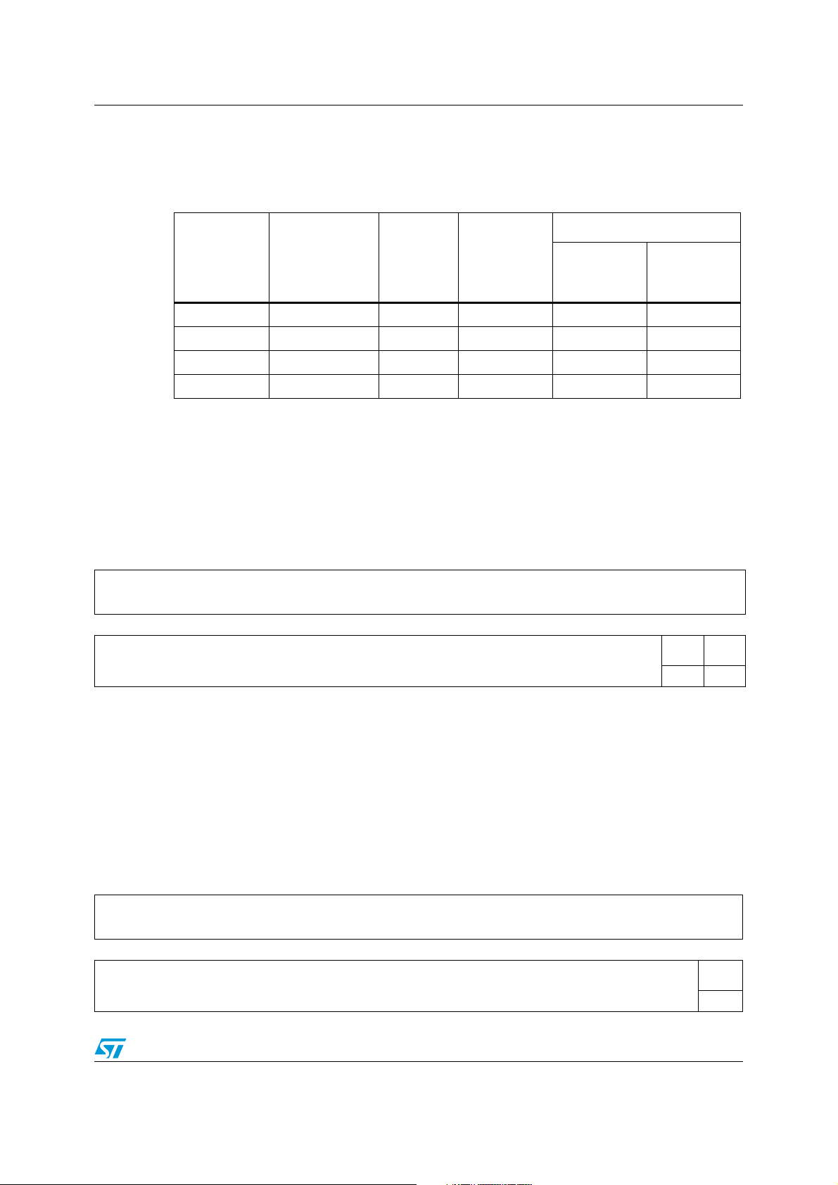
STM32W108C8 System modules
In addition to these modes, further automatic control is invoked by hardware when flash
programming is enabled. To ensure accuracy of the flash controller's timers, the FCLK
frequency is forced to 12 MHz during flash programming and erase operations.
Table 5. System clock modes
f
CLK
OSC24M_SEL CPU_CLK_SEL SCLK PCLK
Flash
Program/
Erase Inactive
Flash
Program/
Erase Active
0 (OSCHF) 0 (Normal CPU) 12 MHz 6 MHz 6 MHz 12 MHz
0 (OSCHF) 1 (Fast CPU) 12 MHz 6 MHz 12 MHz 12 MHz
1 (OSC24M) 0 (Normal CPU) 24 MHz 12 MHz 12 MHz 12 MHz
1 (OSC24M) 1 (Fast CPU) 24 MHz 12 MHz 24 MHz 12 MHz
6.3.6 Clock switching registers
XTAL or OSCHF main clock select register (OSC24M_CTRL)
Address offset: 0x4000 401C
Reset value: 0x0000 0000
Table 6. XTAL or OSCHF main clock select register (OSC24M_CTRL)
31 30 29 28 27 26 25 24 23 22 21 20 19 18 17 16
15 14 13 12 11 10 9 8 7 6 5 4 3 2 1 0
Reserved
Reserved
Bit 1 OSC24M_EN: When set to ‘1’, 24 MHz crystal oscillator is main clock.
OSC24
M_EN
rws rws
OSC24
M_SEL
Bit 0 OSC24M_SEL: When set to ‘0’, OSCHF is selected. When set to ‘1’, XTAL is selected.
CPU clock source select register (CPU_CLK_SEL)
Address offset: 0x4000 4020
Reset value: 0x0000 0000
Table 7. CPU clock source select register (CPU_CLK_SEL)
31 30 29 28 27 26 25 24 23 22 21 20 19 18 17 16
15 14 13 12 11 10 9 8 7 6 5 4 3 2 1 0
Reserved
Rserved
Doc ID 018587 Rev 2 40/215
CPU_C
LK_SEL
rws
Page 42

System modules STM32W108C8
Bit 0 CPU_CLK_SEL: When set to ‘0’, 12-MHz CPU clock is selected. When set to ‘1’, 24-MHz CPU
clock is selected. Note that the clock selection also determines if RAM controller is running at
the same speed as the HCLK (CPU_CLK_SEL = ‘1’) or double speed of HCLK (CPU_CLK_SEL
= ‘0’).
6.4 System timers
6.4.1 Watchdog timer
The STM32W108C8 integrates a watchdog timer which can be enabled to provide
protection against software crashes and ARM® Cortex-M3 CPU lockup. By default, it is
disabled at power up of the always-on power domain. The watchdog timer uses the
calibrated 1 kHz clock (CLK1K) as its reference and provides a nominal 2.048 s timeout. A
low water mark interrupt occurs at 1.792 s and triggers an NMI to the ARM® Cortex-M3
NVIC as an early warning. When enabled, periodically reset the watchdog timer by writing to
the WDOG_RESTART register before it expires.
The watchdog timer can be paused when the debugger halts the ARM® Cortex-M3. To
enable this functionality, set the bit DBG_PAUSE in the SLEEP_CONFIG register.
If the low-frequency internal RC oscillator (OSCRC) is turned off during deep sleep, CLK1K
stops. As a consequence the watchdog timer stops counting and is effectively paused
during deep sleep.
The watchdog enable/disable bits are protected from accidental change by requiring a two
step process. To enable the watchdog timer the application must first write the enable code
0xEABE to the WDOG_CTRL register and then set the WDOG_EN register bit. To disable
the timer the application must write the disable code 0xDEAD to the WDOG_CTRL register
and then set the WDOG_DIS register bit.
6.4.2 Sleep timer
The STM32W108C8 integrates a 32-bit timer dedicated to system timing and waking from
sleep at specific times. The sleep timer can use either the calibrated 1 kHz
reference(CLK1K), or the 32 kHz crystal clock (CLK32K). The default clock source is the
internal 1 kHz clock. The sleep timer clock source is chosen with the SLEEPTMR_CLKSEL
register.
The sleep timer has a prescaler, a divider of the form 2^N, where N can be programmed
from 1 to 2^15. This divider allows for very long periods of sleep to be timed. The timer
provides two compare outputs and wrap detection, all of which can be used to generate an
interrupt or a wake up event.
The sleep timer is paused when the debugger halts the ARM® Cortex-M3. No additional
register bit must be set.
To save current during deep sleep, the low-frequency internal RC oscillator (OSCRC) can
be turned off. If OSCRC is turned off during deep sleep and a low-frequency 32.768 kHz
crystal oscillator is not being used, then the sleep timer will not operate during deep sleep
and sleep timer wake events cannot be used to wakeup the STM32W108C8.
41/215 Doc ID 018587 Rev 2
Page 43
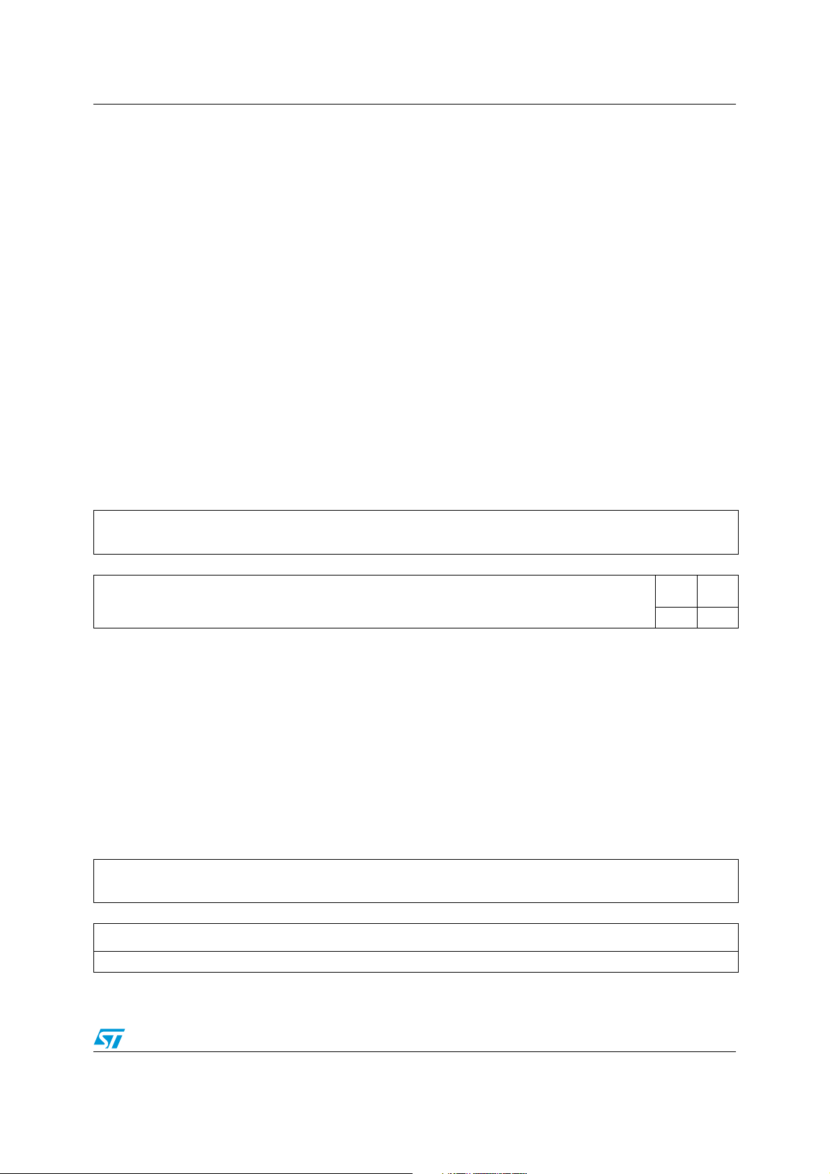
STM32W108C8 System modules
6.4.3 Event timer
The SysTick timer is an ARM® standard system timer in the NVIC. The SysTick timer can
be clocked from either the FCLK (the clock going into the CPU) or the Sleep Timer clock.
FCLK is either the SCLK or PCLK as selected by CPU_CLK_SEL (see Section 6.3.5: Clock
switching on page 39).
6.4.4 Slow timers (Watchdog and Sleeptimer) control and status registers
These registers are powered from the always-on power domain.
All registers are only writable when in System mode
Watchdog general control register (WDOG_CFG)
Register bits for general top level chip functions and protection.
Watchdog bits can only be written after first writing the appropriate code to the
WDOG_CTRL register.
Address: 0x4000 6000
Reset value: 0x0000 0002
Table 8. Watchdog general control register (WDOG_CFG)
31 30 29 28 27 26 25 24 23 22 21 20 19 18 17 16
Reserved
15 14 13 12 11 10 9 8 7 6 5 4 3 2 1 0
WDOG
Reserved
_DIS
rw rw
Bit 1 WDOG_DIS: Watchdog disable
Bit 0 WDOG_EN: Watchdog enable
Watchdog control register (WDOG_CTRL)
Requires magic number write to arm the watchdog enable or disable function.
Address: 0x4000 6004
Reset value: 0x0000 0000
Table 9. Watchdog control register (WDOG_CTRL)
31 30 29 28 27 26 25 24 23 22 21 20 19 18 17 16
15 14 13 12 11 10 9 8 7 6 5 4 3 2 1 0
Reserved
WDOG
_EN
WDOG_CTRL
w
Doc ID 018587 Rev 2 42/215
Page 44

System modules STM32W108C8
Bits [15:0] WDOG_CTRL: Write 0xDEAD to disable or 0xEABE to enable.
Watchdog restart register (WDOG_RESTART)
Write any value to this register to kick-start the watchdog.
Address: 0x4000 6008
Reset value: 0x0000 0000
Sleep timer configuration register (SLEEPTMR_CFG)
This register sets the various options for the Sleep timer.
Address: 0x4000 600C
Reset value: 0x0000 0400
Table 10. Sleep timer configuration register (SLEEPTMR_CFG)
31 30 29 28 27 26 25 24 23 22 21 20 19 18 17 16
15 14 13 12 11 10 9 8 7 6 5 4 3 2 1 0
Reserved
SLEEP
Reserved
rrwrwrwr rw r rw
TMR_
REVER
SE
SLEEP
TMR_
ENABL
E
SLEEP
TMR_
DBGPA
USE
Reserved SLEEPTMR_CLKDIV Reserved
SLEEP
TMR_
CLKSE
Bit 12 SLEEPTMR_REVERSE:
0: count forward; 1: count backwards.
Only changes when ENABLE bit is set to ‘0’.
Bit 11 SLEEPTMR_ENABLE:
0: disable sleep timer; 1: enable sleep timer.
To change other register bits (REVERSE, CLK_DIV, CLK_SEL), this bit must be set to ‘0’.
Enabling/Disabling latency can be up 2 to 3 clock-periods of selected clock.
Bit 10 SLEEPTMR_DBGPAUSE: Debug Pause
0: The timer continues working in Debug mode.
1: The timer is paused in Debug mode when the CPU is halted.
Bits [7:4] SLEEPTMR_CLKDIV: Sleep timer prescaler setting
N
Divides clock by 2
where N = 0 to 15.
Can only be changed when the ENABLE bit is set to ‘0’.
Bit 0 SLEEPTMR_CLKSEL: Clock Select
0: Calibrated 1kHz RC clock (default); 1: 32kHz
Can only be changed when the ENABLE bit is set to ‘0’.
L
Sleep timer count high register (SLEEPTMR_CNTH)
Address: 0x4000 6010
Reset value: 0x0000 0000
43/215 Doc ID 018587 Rev 2
Page 45

STM32W108C8 System modules
Table 11. Sleep timer count high register (SLEEPTMR_CNTH)
31 30 29 28 27 26 25 24 23 22 21 20 19 18 17 16
15 14 13 12 11 10 9 8 7 6 5 4 3 2 1 0
Reserved
SLEEPTMR_CNTH
r
Bits [15:0] SLEEPTMR_CNTH_FIELD:
Sleep timer counter high value [31:16].
Reading this register updates the SLEEP_COUNT_L for subsequent reads.
Sleep timer count low register (SLEEPTMR_CNTL)
Address: 0x4000 6014
Reset value: 0x0000 0000
Table 12. Sleep timer count low register (SLEEPTMR_CNTL)
31 30 29 28 27 26 25 24 23 22 21 20 19 18 17 16
Reserved
15 14 13 12 11 10 9 8 7 6 5 4 3 2 1 0
SLEEPTMR_CNTL
r
Bits [15:0] SLEEPTMR_CNTL_FIELD:
Sleep timer counter low value [15:16].
This register is only valid following a read of the SLEEPTMR_CNTH register.
Sleep timer compare A high register (SLEEPTMR_CMPAH)
Address: 0x4000 6018
Reset value: 0x0000 FFFF
Table 13. Sleep timer compare A high register (SLEEPTMR_CMPAH)
31 30 29 28 27 26 25 24 23 22 21 20 19 18 17 16
15 14 13 12 11 10 9 8 7 6 5 4 3 2 1 0
Reserved
SLEEPTMR_CMPAH
rw
Doc ID 018587 Rev 2 44/215
Page 46

System modules STM32W108C8
Bits [15:0] SLEEPTMR_CMPAH_FIELD:
Sleep timer compare A high value [31:16].
Sleep timer compare value, writing updates COMP_A_H (directly) and COMP_A_L (from
hold register).
Can only be changed when the ENABLE bit (bit 11 of SLEEP_CONFIG register) is set to ‘0’.
If changed when the ENABLE bit is set to ‘1’, a spurious interrupt may be generated.
Therefore it is recommended to disable interrupts before changing this register.
Sleep timer compare A low register (SLEEPTMR_CMPAL)
Address: 0x4000 601C
Reset value: 0x0000 FFFF
Table 14. Sleep timer compare A low register (SLEEPTMR_CMPAL)
31 30 29 28 27 26 25 24 23 22 21 20 19 18 17 16
15 14 13 12 11 10 9 8 7 6 5 4 3 2 1 0
Reserved
SLEEPTMR_CMPAL
rw
Bits [15:0] SLEEPTMR_CMPAL_FIELD:
Sleep timer compare A low value [15:0].
Writing to this register puts value in hold register until a write to the SLEEPTMR_CMPAH
register.
Can only be changed when the ENABLE bit (bit 11 of SLEEP_CONFIG register) is set to ‘0’.
If changed when the ENABLE bit is set to ‘1’, a spurious interrupt may be generated.
Therefore it is recommended to disable interrupts before changing this register.
Sleep timer compare B high register (SLEEPTMR_CMPBH)
Address: 0x4000 6020
Reset value: 0x0000 FFFF
Table 15. Sleep timer compare B high register (SLEEPTMR_CMPBH)
31 30 29 28 27 26 25 24 23 22 21 20 19 18 17 16
15 14 13 12 11 10 9 8 7 6 5 4 3 2 1 0
Reserved
SLEEPTMR_CMPBH
rw
45/215 Doc ID 018587 Rev 2
Page 47

STM32W108C8 System modules
Bits [15:0] SLEEPTMR_CMPBH_FIELD:
Sleep timer compare B high value [31:16].
Sleep timer compare value, writing updates COMP_B_H (directly) and COMP_B_L (from
hold register).
Can only be changed when the ENABLE bit (bit 11 of SLEEP_CONFIG register) is set to ‘0’.
If changed when the ENABLE bit is set to ‘1’, a spurious interrupt may be generated.
Therefore it is recommended to disable interrupts before changing this register.
Sleep timer compare B low register (SLEEPTMR_CMPBL)
Address: 0x4000 6024
Reset value: 0x0000 FFFF
Table 16. Sleep timer compare B low register (SLEEPTMR_CMPBL)
31 30 29 28 27 26 25 24 23 22 21 20 19 18 17 16
15 14 13 12 11 10 9 8 7 6 5 4 3 2 1 0
Reserved
SLEEPTMR_CMPBL
rw
Bits [15:0] SLEEPTMR_CMPBL_FIELD:
Sleep timer compare B low value [15:0].
Writing to this register puts value in hold register until a write to the SLEEPTMR_CMPBH
register.
Can only be changed when the ENABLE bit (bit 11 of SLEEP_CONFIG register) is set to ‘0’.
If changed when the ENABLE bit is set to ‘1’, a spurious interrupt may be generated.
Therefore it is recommended to disable interrupts before changing this register.
Sleep timer interrupt source register (INT_SLEEPTMRFLAG)
Address: 0x4000 A014
Reset value: 0x0000 0000
Table 17. Sleep timer interrupt source register (INT_SLEEPTMRFLAG)
31 30 29 28 27 26 25 24 23 22 21 20 19 18 17 16
15 14 13 12 11 10 9 8 7 6 5 4 3 2 1 0
Reserved
INT_
TMR
INT_
SLEEP
TMR
CMPA
Reserved
rrwrwrw
SLEEP
CMPB
INT_
SLEEP
TMR
WRAP
Doc ID 018587 Rev 2 46/215
Page 48
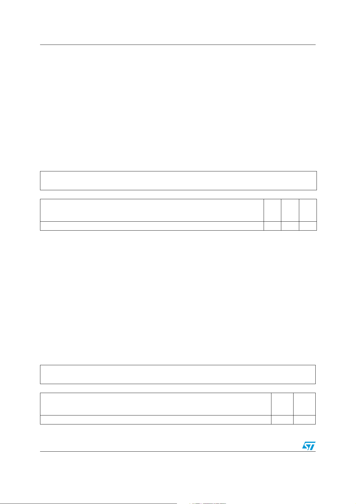
System modules STM32W108C8
Bit 2 INT_ SLEEPTMR CMPB: Sleep timer compare B
Note: Bits are cleared when set to ‘1’.
Bit 1 INT_SLEEPTMRCMPA: Sleep timer compare A
Note: Bits are cleared when set to ‘1’.
Bit 0 INT_SLEEPTMRWRAP: Sleep timer overflow
Note: Bits are cleared when set to ‘1’.
Sleep timer interrupt mask register (INT_SLEEPTMRCFG)
Address: 0x4000 A054
Reset value: 0x0000 0000
Table 18. Sleep timer interrupt mask register (INT_SLEEPTMRCFG)
31 30 29 28 27 26 25 24 23 22 21 20 19 18 17 16
15 14 13 12 11 10 9 8 7 6 5 4 3 2 1 0
Reserved
Reserved
rrwrwrw
Bit 2 INT_ SLEEPTMR CMPB: Sleep timer compare B
INT_
SLEEP
TMR
CMPB
INT_
SLEEP
TMR
CMPA
INT_
SLEEP
TMR
WRAP
Bit 1 INT_SLEEPTMRCMPA: Sleep timer compare A
Bit 0 INT_SLEEPTMRWRAP: Sleep timer overflow
Sleep timer clock source enables (SLEEPTMR_CLKEN)
This timer controls the low power clock gated modes.
Clearing CLKRC_EN before executing WFE with SLEEPDEEP bit set in the NVIC System
control register causes DEEP_SLEEP2 to be entered. Setting this bit causes
DEEP_SLEEP1 to be entered.
Address: 0x4000 0008
Reset value: 0x0000 0002
Table 19. Sleep timer clock source enables (SLEEPTMR_CLKEN)
31 30 29 28 27 26 25 24 23 22 21 20 19 18 17 16
15 14 13 12 11 10 9 8 7 6 5 4 3 2 1 0
Reserved
SLEEP
Reserved
rrwrw
TMR_
CLK10K
EN
SLEEP
TMR_
CLK32K
EN
47/215 Doc ID 018587 Rev 2
Page 49

STM32W108C8 System modules
Bit 1 SLEEPTMR_CLK10KEN: Enables 10kHz internal RC during deep
Note: Bits are cleared when set to ‘1’.
Bit 0 SLEEPTMR_CLK32KEN: Enables 32kHz external XTAL
Note: Bits are cleared when set to ‘1’.
6.5 Power management
The STM32W108C8's power management system is designed to achieve the lowest deep
sleep current consumption possible while still providing flexible wakeup sources, timer
activity, and debugger operation. The STM32W108C8 has four main sleep modes:
● Idle Sleep: Puts the CPU into an idle state where execution is suspended until any
interrupt occurs. All power domains remain fully powered and nothing is reset.
● Deep Sleep 1: The primary deep sleep state. In this state, the core power domain is
fully powered down and the sleep timer is active
● Deep Sleep 2: The same as Deep Sleep 1 except that the sleep timer is inactive to
save power. In this mode the sleep timer cannot wakeup the STM32W108C8.
● Deep Sleep 0 (also known as Emulated Deep Sleep): The chip emulates a true deep
sleep without powering down the core domain. Instead, the core domain remains
powered and all peripherals except the system debug components (ITM, DWT, FPB,
NVIC) are held in reset. The purpose of this sleep state is to allow STM32W108C8
software to perform a deep sleep cycle while maintaining debug configuration such as
breakpoints.
6.5.1 Wake sources
When in deep sleep the STM32W108C8 can be returned to the running state in a number of
ways, and the wake sources are split depending on deep sleep 1 or deep sleep 2.
The following wake sources are available in both deep sleep 1 and 2.
● Wake on GPIO activity: Wake due to change of state on any GPIO.
● Wake on serial controller 1: Wake due to a change of state on GPIO Pin PB2.
● Wake on serial controller 2: Wake due to a change of state on GPIO Pin PA2.
● Wake on IRQD: Wake due to a change of state on IRQD. Since IRQD can be
configured to point to any GPIO, this wake source is another means of waking on any
GPIO activity.
● Wake on setting of CDBGPWRUPREQ: Wake due to setting the CDBGPWRUPREQ bit
in the debug port in the SWJ.
● Wake on setting of CSYSPWRUPREQ: Wake due to setting the CSYSPWRUPREQ bit
in the debug port in the SWJ.
The following sources are only available in deep sleep 1 since the sleep timer is not active in
deep sleep 2.
● Wake on sleep timer compare A.
● Wake on sleep timer compare B.
● Wake on sleep timer wrap.
Doc ID 018587 Rev 2 48/215
Page 50

System modules STM32W108C8
The following source is only available in deep sleep 0 since the SWJ is required to write
memory to set this wake source and the SWJ only has access to some registers in deep
sleep 0.
● Wake on write to the WAKE_CORE register bit.
The Wakeup Recording module monitors all possible wakeup sources. More than one
wakeup source may be recorded because events are continually being recorded (not just in
deep-sleep), since another event may happen between the first wake event and when the
STM32W108C8 wakes up.
49/215 Doc ID 018587 Rev 2
Page 51

STM32W108C8 System modules
6.5.2 Basic sleep modes
The power management state diagram in Figure 6 shows the basic operation of the power
management controller.
Figure 6. Power management state diagram
CDBGPWRU PREQ set
DEEP SLEEP
CDBGPWRUPREQ=0
& CSYSP WRUPREQ=0
PRE- DEEP
SLEEP
CSYSPWRUPR EQ & INHIBIT
CDBGPWRU PREQ cleare d
=
Q
E
R
Q
P
E
U
R
R
P
W
U
R
P
G
W
B
P
D
S
C
Y
S
C
&
(
r
e
Deep sleep requested
(WFI instru ction with SLEEP_DEEP= 1)
Sleep
uc
r
nst
i
I
WF
(
EMULAT ED
DEEP SLEEP
1
0
=
Wake up event
(resets the processor)
OR CSYSPWRUPREQ set
W
a
k
s
e
e
u
t
s
p
t
e
h
e
v
e
p
n
r
o
t
c
e
s
s
o
r
)
RUNNING
0)
P=
E
E
d
_D
e
t
P
s
E
LE
eque
S
r
ith
w
n
tio
t
p
Interru
IDLE SLEEP
Doc ID 018587 Rev 2 50/215
Page 52

System modules STM32W108C8
In normal operation an application may request one of two low power modes through
program execution:
● Idle Sleep is achieved by executing a WFI instruction whilst the SLEEPDEEP bit in the
Cortex System Control register (SCS_SCR) is clear. This puts the CPU into an idle
state where execution is suspended until an interrupt occurs. This is indicated by the
state at the bottom of the diagram. Power is maintained to the core logic of the
STM32W108C8 during the Idle Sleeping state.
● Deep sleep is achieved by executing a WFI instruction with the SLEEPDEEP bit in
SCS_SCR set. This triggers the state transitions around the main loop of the diagram,
resulting in powering down the STM32W108C8's core logic, and leaving only the
always-on domain powered. Wake up is triggered when one of the pre-determined
events occurs.
If a deep sleep is requested the STM32W108C8 first enters a pre-deep sleep state. This
state prevents any section of the chip from being powered off or reset until the SWJ goes
idle (by clearing CSYSPWRUPREQ). This pre-deep sleep state ensures debug operations
are not interrupted.
In the deep sleep state the STM32W108C8 waits for a wake up event which will return it to
the running state. In powering up the core logic the ARM® Cortex-M3 is put through a reset
cycle and ST software restores the stack and application state to the point where deep sleep
was invoked.
6.5.3 Further options for deep sleep
By default, the low-frequency internal RC oscillator (OSCRC) is running during deep sleep
(known as deep sleep 1).
To conserve power, OSCRC can be turned off during deep sleep. This mode is known as
deep sleep 2. Since the OSCRC is disabled, the sleep timer and watchdog timer do not
function and cannot wake the chip unless the low-frequency 32.768 kHz crystal oscillator is
used. Non-timer based wake sources continue to function. Once a wake event occurs, the
OSCRC restarts and becomes enabled.
6.5.4 Use of debugger with sleep modes
The debugger communicates with the STM32W108C8 using the SWJ.
When the debugger is connected, the CDBGPWRUPREQ bit in the debug port in the SWJ
is set, the STM32W108C8 will only enter deep sleep 0 (the Emulated Deep Sleep state).
The CDBGPWRUPREQ bit indicates that a debug tool is connected to the chip and
therefore there may be debug state in the system debug components. To maintain the state
in the system debug components only deep sleep 0 may be used, since deep sleep 0 will
not cause a power cycle or reset of the core domain. The CSYSPWRUPREQ bit in the
debug port in the SWJ indicates that a debugger wants to access memory actively in the
STM32W108C8. Therefore, whenever the CSYSPWRUPREQ bit is set while the
STM32W108C8 is awake, the STM32W108C8 cannot enter deep sleep until this bit is
cleared. This ensures the STM32W108C8 does not disrupt debug communication into
memory.
Clearing both CSYSPWRUPREQ and CDBGPWRUPREQ allows the STM32W108C8 to
achieve a true deep sleep state (deep sleep 1 or 2). Both of these signals also operate as
wake sources, so that when a debugger connects to the STM32W108C8 and begins
accessing the chip, the STM32W108C8 automatically comes out of deep sleep. When the
51/215 Doc ID 018587 Rev 2
Page 53

STM32W108C8 System modules
debugger initiates access while the STM32W108C8 is in deep sleep, the SWJ intelligently
holds off the debugger for a brief period of time until the STM32W108C8 is properly
powered and ready.
For more information regarding the SWJ and the interaction of debuggers with deep sleep,
contact ST support for Application Notes and ARM® CoreSight documentation.
6.6 Security accelerator
The STM32W108C8 contains a hardware AES encryption engine accessible from the
ARM® Cortex-M3. NIST-based CCM, CCM*, CBC-MAC, and CTR modes are implemented
in hardware. These modes are described in the IEEE 802.15.4-2003 specification, with the
exception of CCM*, which is described in the ZigBee Security Services Specification 1.0.
Doc ID 018587 Rev 2 52/215
Page 54

Integrated voltage regulator STM32W108C8
7 Integrated voltage regulator
The STM32W108C8 integrates two low dropout regulators to provide 1.8 V and 1.25 V
power supplies. The 1V8 regulator supplies the analog and memories, and the 1V25
regulator supplies the digital core. In deep sleep the voltage regulators are disabled.
When enabled, the 1V8 regulator steps down the pads supply voltage (VDD_PADS) from a
nominal 3.0 V to 1.8 V. The regulator output pin (VREG_OUT) must be decoupled externally
with a suitable capacitor. VREG_OUT should be connected to the 1.8 V supply pins VDDA,
VDD_RF, VDD_VCO, VDD_SYNTH, VDD_IF, and VDD_MEM. The 1V8 regulator can
supply a maximum of 50 mA.
When enabled, the 1V25 regulator steps down VDD_PADS to 1.25 V. The regulator output
pin (VDD_CORE, (Pin 17) must be decoupled externally with a suitable capacitor. It should
connect to the other VDD_CORE pin (Pin 44). The 1V25 regulator can supply a maximum of
10 mA.
The regulators are controlled by the digital portion of the chip as described in Section 6:
System modules.
Table 20. 1.8 V integrated voltage regulator specifications
Parameter Min. Typ. Max. Units Comments
Supply range for regulator 2.1 3.6 V VDD_PADS
1V8 regulator output -5% 1.8 +5% V
1V8 regulator output after reset -5% 1.75 +5%
1V25 regulator output -5% 1.25 +5% V
1V25 regulator output after reset -5% 1.45 +5%
1V8 regulator capacitor 2.2 µF
1V25 regulator capacitor 1.0 µF Ceramic capacitor (0603)
1V8 regulator output current 0 50 mA Regulator output current
1V25 regulator output current 0 10 mA Regulator output current
No load current 600 µA
1V8 regulator current limit 200 mA Short circuit current limit
1V25 regulator current limit 25 mA Short circuit current limit
Regulator output after
initialization
Regulator output after
reset
Regulator output after
initialization
Regulator output after
reset
Low ESR tantalum
capacitor
ESR greater than 2 Ω
ESR less than 10 Ω
De-coupling less than100
nF ceramic
No load current
(bandgap and regulators)
53/215 Doc ID 018587 Rev 2
Page 55

STM32W108C8 Integrated voltage regulator
Table 20. 1.8 V integrated voltage regulator specifications (continued)
Parameter Min. Typ. Max. Units Comments
1V8 regulator start-up time 50 µs
1V25 regulator start-up time 50 µs
0 V to POR threshold 2.2
µF capacitor
0 V to POR threshold 1.0
µF capacitor
An external 1.8 V regulator may replace both internal regulators. The STM32W108C8 can
control external regulators during deep sleep using open-drain GPIO PA7, as described in
Section 8: General-purpose input/outputs. The STM32W108C8 drives PA7 low during deep
sleep to disable the external regulator and an external pull-up is required to release this
signal to indicate that supply voltage should be provided. Current consumption increases
approximately 2 mA when using an external regulator. When using an external regulator the
internal regulators should be disabled through software.
Doc ID 018587 Rev 2 54/215
Page 56

General-purpose input/outputs STM32W108C8
8 General-purpose input/outputs
The STM32W108C8 has 24 multi-purpose GPIO pins that may be individually configured
as:
● General purpose output
● General purpose open-drain output
● Alternate output controlled by a peripheral device
● Alternate open-drain output controlled by a peripheral device
● Analog
● General purpose input
● General purpose input with pull-up or pull-down resistor
The basic structure of a single GPIO is illustrated in Figure 7.
Figure 7. GPIO block diagram
GPIO_ PxCFGH/L
GPIO _PxSET
GPIO_PxC LR
GPIO_PxOU T
Alt ernat e output
Alt ernat e input
Wake detection
GPIO_PxIN
Output c ontrol
(pus h pull ,
open drai n , or
dis abled )
GPIO_PxW AKE
VDD _PADS
P-M OS
N-MOS
GND
Schmitt tr igger
VDD _PADS
GND
Analog
functi ons
VDD _PADS
Prot ection
Prot ection
GND
diode
PIN
diode
A Schmitt trigger converts the GPIO pin voltage to a digital input value. The digital input
signal is then always routed to the GPIO_PxIN register; to the alternate inputs of associated
peripheral devices; to wake detection logic if wake detection is enabled; and, for certain
pins, to interrupt generation logic. Configuring a pin in analog mode disconnects the digital
input from the pin and applies a high logic level to the input of the Schmitt trigger.
Only one device at a time can control a GPIO output. The output is controlled in normal
output mode by the GPIO_PxOUT register and in alternate output mode by a peripheral
device. When in input mode or analog mode, digital output is disabled.
55/215 Doc ID 018587 Rev 2
Page 57

STM32W108C8 General-purpose input/outputs
8.1 Functional description
8.1.1 GPIO ports
The 24 GPIO pins are grouped into three ports: PA, PB, and PC. Individual GPIOs within a
port are numbered 0 to 7 according to their bit positions within the GPIO registers.
Note: Because GPIO port registers' functions are identical, the notation Px is used here to refer to
PA, PB, or PC. For example, GPIO_PxIN refers to the registers GPIO_PAIN, GPIO_PBIN,
and GPIO_PCIN.
Each of the three GPIO ports has the following registers whose low-order eight bits
correspond to the port's eight GPIO pins:
● GPIO_PxIN (input data register) returns the pin level (unless in analog mode).
● GPIO_PxOUT (output data register) controls the output level in normal output mode.
● GPIO_PxCLR (clear output data register) clears bits in GPIO_PxOUT.
● GPIO_PxSET (set output data register) sets bits in GPIO_PxOUT.
● GPIO_PxWAKE (wake monitor register) specifies the pins that can wake the
STM32W108C8.
In addition to these registers, each port has a pair of configuration registers,
GPIO_PxCFGH and GPIO_PxCFGL. These registers specify the basic operating mode for
the port's pins. GPIO_PxCFGL configures the pins Px[3:0] and GPIO_PxCFGH configures
the pins Px[7:4]. For brevity, the notation GPIO_PxCFGH/L refers to the pair of configuration
registers.
Five GPIO pins (PA6, PA7, PB6, PB7 and PC0) can sink and source higher current than
standard GPIO outputs. Refer to Table 150: Digital I/O characteristics on page 205 for more
information.
8.1.2 Configuration
Each pin has a 4-bit configuration value in the GPIO_PxCFGH/L register. The various GPIO
modes and their 4 bit configuration values are shown in Ta bl e 2 1 .
Table 21. GPIO configuration modes
GPIO mode GPIO_PxCFGH/L Description
Analog 0x0
Input (floating) 0x4
Input (pull-up or pulldown)
Output (push-pull) 0x1 Push-pull output. GPIO_PxOUT controls the output.
Output (open-drain) 0x5
Alternate Output (pushpull)
0x8
0x9
Analog input or output. When in analog mode, the
digital input (GPIO_PxIN) always reads 1.
Digital input without an internal pull up or pull down.
Output is disabled.
Digital input with an internal pull up or pull down. A set
bit in GPIO_PxOUT selects pull up and a cleared bit
selects pull down. Output is disabled.
Open-drain output. GPIO_PxOUT controls the output.
If a pull up is required, it must be external.
Push-pull output. An onboard peripheral controls the
output.
Doc ID 018587 Rev 2 56/215
Page 58
General-purpose input/outputs STM32W108C8
Table 21. GPIO configuration modes (continued)
GPIO mode GPIO_PxCFGH/L Description
Alternate Output (opendrain)
Alternate Output (pushpull) SPI SCLK Mode
0xD
0xB
Open-drain output. An onboard peripheral controls the
output. If a pull up is required, it must be external.
Push-pull output mode only for SPI master mode
SCLK pins.
If a GPIO has two peripherals that can be the source of alternate output mode data, then
other registers in addition to GPIO_PxCFGH/L determine which peripheral controls the
output.
Several GPIOs share an alternate output with Timer 2 and the Serial Controllers. Bits in
Timer 2's TIM2_OR register control routing Timer 2 outputs to different GPIOs. Bits in Timer
2's TIM2_CCER register enable Timer 2 outputs. When Timer 2 outputs are enabled they
override Serial Controller outputs. Ta bl e 2 2 indicates the GPIO mapping for Timer 2 outputs
depending on the bits in the register TIM2_OR. Refer to Section 10: General-purpose timers
on page 109 for complete information on timer configuration.
Table 22. Timer 2 output configuration controls
GPIO mapping selected by TIM2_OR bit
Timer 2 output Option register bit
01
TIM2_CH1 TIM2_OR[4] PA0 PB1
TIM2_CH2 TIM2_OR[5] PA3 PB2
TIM2_CH3 TIM2_OR[6] PA1 PB3
TIM2_CH4 TIM2_OR[7] PA2 PB4
For outputs assigned to the serial controllers, the serial interface mode registers
(SCx_MODE) determine how the GPIO pins are used.
The alternate outputs of PA4 and PA5 can either provide packet trace data (PTI_EN and
PTI_DATA), or synchronous CPU trace data (TRACEDATA2 and TRACEDATA3).
If a GPIO does not have an associated peripheral in alternate output mode, its output is set
to 0.
8.1.3 Forced functions
For some GPIOs the GPIO_PxCFGH/L configuration may be overridden. Ta b le 2 3 shows
the GPIOs that can have different functions forced on them regardless of the
GPIO_PxCFGH/L registers.
Note: The DEBUG_DIS bit in the GPIO_DBGCFG register can disable the Serial Wire/JTAG
debugger interface. When this bit is set, all debugger-related pins (PC0, PC2, PC3, PC4)
behave as standard GPIO.
57/215 Doc ID 018587 Rev 2
Page 59

STM32W108C8 General-purpose input/outputs
Table 23. GPIO forced functions
GPIO Override condition Forced function Forced signal
GPIO_EXTREGEN bit set in the
PA 7
GPIO_DBGCFG register
PC0 Debugger interface is active in JTAG mode Input with pull up JRST
PC2 Debugger interface is active in JTAG mode Push-pull output JTDO
PC3 Debugger interface is active in JTAG mode Input with pull up JDTI
PC4 Debugger interface is active in JTAG mode Input with pull up JTMS
Debugger interface is active in Serial Wire
PC4
mode
Open-drain output REG_EN
Bidirectional (push-pull
output or floating input)
controlled by debugger
interface
SWDIO
8.1.4 Reset
A full chip reset is one due to power on (low or high voltage), the NRST pin, the watchdog, or
the SYSRESETREQ bit. A full chip reset affects the GPIO configuration as follows:
● The GPIO_PxCFGH/L configurations of all pins are configured as floating inputs.
● The GPIO_EXTREGEN bit is set in the GPIO_DBGCFG register, which overrides the
normal configuration for PA7.
● The GPIO_DEBUGDIS bit in the GPIO_DBGCFG register is cleared, allowing Serial
Wire/JTAG access to override the normal configuration of PC0, PC2, PC3, and PC4.
8.1.5 nBOOTMODE
nBOOTMODE is a special alternate function of PA5 that is active only during a pin reset
(NRST) or a power-on-reset of the always-powered domain (POR_HV). If nBOOTMODE is
asserted (pulled or driven low) when coming out of reset, the processor starts executing an
embedded serial boot loader instead of its normal program.
While in reset and during the subsequent power-on-reset startup delay (512 high-frequency
RC oscillator periods), PA5 is automatically configured as an input with a pull-up resistor. At
the end of this time, the STM32W108C8 samples nBOOTMODE: a high level selects normal
startup, and a low level selects the boot loader. After nBOOTMODE has been sampled, PA5
is configured as a floating input. The GPIO_BOOTMODE bit in the GPIO_DBGSTAT register
captures the state of nBOOTMODE so that software may act on this signal if required.
Note: To avoid inadvertently asserting nBOOTMODE, PA5's capacitive load should not exceed
252 pF.
Doc ID 018587 Rev 2 58/215
Page 60

General-purpose input/outputs STM32W108C8
8.1.6 GPIO modes
Analog mode
Analog mode enables analog functions, and disconnects a pin from the digital input and
output logic. Only the following GPIO pins have analog functions:
● PA4, PA5, PB5, PB6, PB7, and PC1 can be analog inputs to the ADC.
● PB0 can be an external analog voltage reference input to the ADC, or it can output the
internal analog voltage reference from the ADC.
● PC6 and PC7 can connect to an optional 32.768 kHz crystal.
Note: When an external timing source is required, a 32.768 kHz crystal is commonly connected to
PC6 and PC7. Alternatively, when PC7 is configured as a digital input, PC7 can accept a
digital external clock input.
When configured in analog mode:
● The output drivers are disabled.
● The internal pull-up and pull-down resistors are disabled.
● The Schmitt trigger input is connected to a high logic level.
● Reading GPIO_PxIN returns a constant 1.
Input mode
Input mode is used both for general purpose input and for on-chip peripheral inputs. Input
floating mode disables the internal pull-up and pull-down resistors, leaving the pin in a highimpedance state. Input pull-up or pull-down mode enables either an internal pull-up or pulldown resistor based on the GPIO_PxOUT register. Setting a bit to 0 in GPIO_PxOUT
enables the pull-down and setting a bit to 1 enables the pull up.
When configured in input mode:
● The output drivers are disabled.
● An internal pull-up or pull-down resistor may be activated depending on
GPIO_PxCFGH/L and GPIO_PxOUT.
● The Schmitt trigger input is connected to the pin.
● Reading GPIO_PxIN returns the input at the pin.
● The input is also available to on-chip peripherals.
Output mode
Output mode provides a general purpose output under direct software control. Regardless
of whether an output is configured as push-pull or open-drain, the GPIO's bit in the
GPIO_PxOUT register controls the output. The GPIO_PxSET and GPIO_PxCLR registers
can atomically set and clear bits within GPIO_PxOUT register. These set and clear registers
simplify software using the output port because they eliminate the need to disable interrupts
to perform an atomic read-modify-write operation of GPIO_PxOUT.
59/215 Doc ID 018587 Rev 2
Page 61

STM32W108C8 General-purpose input/outputs
When configured in output mode:
● The output drivers are enabled and are controlled by the value written to
GPIO_PxOUT:
● In open-drain mode: 0 activates the N-MOS current sink; 1 tri-states the pin.
● In push-pull mode: 0 activates the N-MOS current sink; 1 activates the P-MOS current
source.
● The internal pull-up and pull-down resistors are disabled.
● The Schmitt trigger input is connected to the pin.
● Reading GPIO_PxIN returns the input at the pin.
● Reading GPIO_PxOUT returns the last value written to the register.
Note: Depending on configuration and usage, GPIO_PxOUT and GPIO_PxIN may not have the
same value.
Alternate output mode
In this mode, the output is controlled by an on-chip peripheral instead of GPIO_PxOUT and
may be configured as either push-pull or open-drain. Most peripherals require a particular
output type - I
does not by itself configure a pin, the GPIO_PxCFGH/L registers must be configured
properly for a peripheral's particular needs. As described in Section 8.1.2: Configuration on
page 56, when more than one peripheral can be the source of output data, registers in
addition to GPIO_PxCFGH/L determine which to use.
2
C requires an open-drain driver, for example - but since using a peripheral
When configured in alternate output mode:
● The output drivers are enabled and are controlled by the output of an on-chip
peripheral:
● In open-drain mode: 0 activates the N-MOS current sink; 1 tri-states the pin.
● In push-pull mode: 0 activates the N-MOS current sink; 1 activates the P-MOS current
source.
● The internal pull-up and pull-down resistors are disabled.
● The Schmitt trigger input is connected to the pin.
● Reading GPIO_PxIN returns the input to the pin.
Note: Depending on configuration and usage, GPIO_PxOUT and GPIO_PxIN may not have the
same value.
Alternate output SPI SCLK mode
SPI master mode SCLK outputs, PB3 (SC1SCLK) or PA2 (SC2SCLK), use a special output
push-pull mode reserved for those signals. Otherwise this mode is identical to alternate
output mode.
8.1.7 Wake monitoring
The GPIO_PxWAKE registers specify which GPIOs are monitored to wake the processor. If
a GPIO's wake enable bit is set in GPIO_PxWAKE, then a change in the logic value of that
GPIO causes the STM32W108C8 to wake from deep sleep. The logic values of all GPIOs
are captured by hardware upon entering sleep. If any GPIO's logic value changes while in
sleep and that GPIO's GPIO_PxWAKE bit is set, then the STM32W108C8 will wake from
deep sleep. (There is no mechanism for selecting a specific rising-edge, falling-edge, or
level on a GPIO: any change in logic value triggers a wake event.) Hardware records the fact
Doc ID 018587 Rev 2 60/215
Page 62

General-purpose input/outputs STM32W108C8
that GPIO activity caused a wake event, but not which specific GPIO was responsible.
Instead, software should read the state of the GPIOs on waking to determine the cause of
the event.
The register GPIO_WAKEFILT contains bits to enable digital filtering of the external wakeup
event sources: the GPIO pins, SC1 activity, SC2 activity, and IRQD. The digital filter
operates by taking samples based on the (nominal) 10 kHz RC oscillator. If three samples in
a row all have the same logic value, and this sampled logic value is different from the logic
value seen upon entering sleep, the filter outputs a wakeup event.
In order to use GPIO pins to wake the STM32W108C8 from deep sleep, the GPIO_WAKE
bit in the WAKE_SEL register must be set. Waking up from GPIO activity does not work with
pins configured for analog mode since the digital logic input is always set to 1 when in
analog mode. Refer to Section 6: System modules on page 32 for information on the
STM32W108C8's power management and sleep modes.
8.2 External interrupts
The STM32W108C8 can use up to four external interrupt sources (IRQA, IRQB, IRQC, and
IRQD), each with its own top level NVIC interrupt vector. Since these external interrupt
sources connect to the standard GPIO input path, an external interrupt pin may
simultaneously be used by a peripheral device or even configured as an output. Analog
mode is the only GPIO configuration that is not compatible with using a pin as an external
interrupt.
External interrupts have individual triggering and filtering options selected using the
registers GPIO_INTCFGA, GPIO_INTCFGB, GPIO_INTCFGC, and GPIO_INTCFGD. The
bit field GPIO_INTMOD of the GPIO_INTCFGx register enables IRQx's second level
interrupt and selects the triggering mode: 0 is disabled; 1 for rising edge; 2 for falling edge; 3
for both edges; 4 for active high level; 5 for active low level. The minimum width needed to
latch an unfiltered external interrupt in both level- and edge-triggered mode is 80 ns. With
the digital filter enabled (the GPIO_INTFILT bit in the GPIO_INTCFGx register is set), the
minimum width needed is 450 ns.
The register INT_GPIOFLAG is the second-level interrupt flag register that indicates
pending external interrupts. Writing 1 to a bit in the INT_GPIOFLAG register clears the flag
while writing 0 has no effect. If the interrupt is level-triggered, the flag bit is set again
immediately after being cleared if its input is still in the active state.
Two of the four external interrupts, IRQA and IRQB, have fixed pin assignments. The other
two external interrupts, IRQC and IRQD, can use any GPIO pin. The GPIO_IRQCSEL and
GPIO_IRQDSEL registers specify the GPIO pins assigned to IRQC and IRQD, respectively.
Ta bl e 2 4 shows how the GPIO_IRQCSEL and GPIO_IRQDSEL register values select the
GPIO pin used for the external interrupt.
Table 24. IRQC/D GPIO selection
GPIO_IRQxSEL GPIO
0 PA0 8 PB0 16 PC0
GPIO_IRQxSE
L
GPIO
GPIO_IRQxSE
L
GPIO
1 PA1 9 PB1 17 PC1
2 PA2 10 PB2 18 PC2
61/215 Doc ID 018587 Rev 2
Page 63

STM32W108C8 General-purpose input/outputs
Table 24. IRQC/D GPIO selection (continued)
GPIO_IRQxSEL GPIO
GPIO_IRQxSE
3 PA3 11 PB3 19 PC3
4 PA4 12 PB4 20 PC4
5 PA5 13 PB5 21 PC5
6 PA6 14 PB6 22 PC6
7 PA7 15 PB7 23 PC7
In some cases, it may be useful to assign IRQC or IRQD to an input also in use by a
peripheral, for example to generate an interrupt from the slave select signal (nSSEL) in an
SPI slave mode interface.
Refer to Section 12: Interrupts on page 174 for further information regarding the
STM32W108C8 interrupt system.
8.3 Debug control and status
Two GPIO registers are largely concerned with debugger functions. GPIO_DBGCFG can
disable debugger operation, but has other miscellaneous control bits as well.
GPIO_DBGSTAT, a read-only register, returns status related to debugger activity
(GPIO_FORCEDBG and GPIO_SWEN), as well a flag (GPIO_BOOTMODE) indicating
whether nBOOTMODE was asserted at the last power-on or NRST-based reset.
L
GPIO
GPIO_IRQxSE
L
GPIO
8.4 GPIO alternate functions
Ta bl e 2 5 lists the GPIO alternate functions.
Table 25. GPIO signal assignments
GPIO Analog Alternate function Input
PA 0
PA 1
PA 2
PA 3
PA4 ADC4 PTI_EN, TRACEDATA2 Standard
PA 5 A D C5
PA6 TIM1_CH3 TIM1_CH3 High
PA 7
TIM2_CH1
SC2MOSI
TIM2_CH3
SC2MISO, SC2SDA
TIM2_CH4
SC2SCLK, SC2SCL
TIM2_CH2
TRACECLK
PTI_DATA,
TRACEDATA3
TIM1_CH4, REG_EN
(3)
(1)
(1)
(1)
(1)
Output current
drive
,
TIM2_CH1
SC2MOSI
,
TIM2_CH3
SC2MISO, SC2SDA
,
TIM2_CH4
SC2SCLK
,
TIM2_CH2
SC2nSSEL
nBOOTMODE
(1)
(1)
(1)
(1)
,
,
,
,
(2)
Standard
Standard
Standard
Standard
Standard
TIM1_CH4 High
Doc ID 018587 Rev 2 62/215
Page 64

General-purpose input/outputs STM32W108C8
Table 25. GPIO signal assignments (continued)
GPIO Analog Alternate function Input
PB0 VREF TRACECLK
TIM2_CH1
PB1
SC1MOSI, SC1MISO,
(4)
, SC1TXD,
TIM1CLK, TIM2MSK,
IRQA
TIM2_CH1
(4)
, SC1SDA Standard
Output current
drive
Standard
SC1SDA
(4)
(4)
(4)
,
Standard
,
,
Standard
Standard
PB2
PB3
PB4
TIM2_CH2
SC1SCLK
TIM2_CH3
SC1SCLK
TIM2_CH4
UART_RTS
(4)
(4)
(4)
,
TIM2_CH2
SC1MISO, SC1MOSI,
SC1SCL, SC1RXD
,
TIM2_CH3
SC1SCLK, UART_CTS
,
TIM2_CH4
SC1nSSEL
PB5 ADC0 TIM2CLK, TIM1MSK Standard
PB6 ADC1 TIM1_CH1 TIM1_CH1, IRQB High
PB7 ADC2 TIM1_CH2 TIM1_CH2 High
PC0 TRACEDATA1 JRST
(5)
High
PC1 ADC3 TRACEDATA0, SWO Standard
PC2 JTDO
PC3 JTDI
PC4 SWDIO
(6)
, SWO Standard
(7)
(5)
SWDIO
(7)
, JTMS
(5)
Standard
Standard
PC5 TX_ACTIVE Standard
PC6 OSC32B nTX_ACTIVE Standard
PC7 OSC32A OSC32_EXT Standard
1. Default signal assignment (not remapped).
2. Overrides during reset as an input with pull up.
3. Overrides after reset as an open-drain output.
4. Alternate signal assignment (remapped).
5. Overrides in JTAG mode as an input with pull up.
6. Overrides in JTAG mode as a push-pull output.
7. Overrides in Serial Wire mode as either a push-pull output, or a floating input, controlled by the debugger.
63/215 Doc ID 018587 Rev 2
Page 65

STM32W108C8 General-purpose input/outputs
8.5 General-purpose input / output (GPIO) registers
8.5.1 Port x configuration register (Low) (GPIO_PxCFGL)
Address offset: 0xB000 (GPIO_PACFGL), 0xB400 (GPIO_PBCFGL) and 0xB800
(GPIO_PCCFGL)
Reset value: 0x0000 4444
Table 26. Port x configuration register (Low) (GPIO_PxCFGL)
31 30 29 28 27 26 25 24 23 22 21 20 19 18 17 16
15 14 13 12 11 10 9 8 7 6 5 4 3 2 1 0
Reserved
Px3_CFG Px2_CFG Px1_CFG Px0_CFG
rw rw rw rw
Bits [15:12] Px3_CFG: GPIO configuration control.
0x0: Analog, input or output (GPIO_PxIN always reads 1).
0x1: Output, push-pull (GPIO_PxOUT controls the output).
0x4: Input, floating.
0x5: Output, open-drain (GPIO_PxOUT controls the output).
0x8: Input, pulled up or down (selected by GPIO_PxOUT: 0 = pull-down, 1 = pull-up).
0x9: Alternate output, push-pull (peripheral controls the output).
0xB: Alternate output SPI SCLK, push-pull (only for SPI master mode SCLK).
0xD: Alternate output, open-drain (peripheral controls the output).
Bits [11:8] Px2_CFG: GPIO configuration control: see Px3_CFG above.
Bits [7:4] Px1_CFG: GPIO configuration control: see Px3_CFG above.
Bits [3:0] Px0_CFG: GPIO configuration control: see Px3_CFG above.
8.5.2 Port x configuration register (High) (GPIO_PxCFGH)
Address offset: 0xB004 (GPIO_PACFGH), 0xB404 (GPIO_PBCFGH) and 0xB804
(GPIO_PCCFGH)
Reset value: 0x0000 4444
Table 27. Port x configuration register (High) (GPIO_PxCFGH)
31 30 29 28 27 26 25 24 23 22 21 20 19 18 17 16
15 14 13 12 11 10 9 8 7 6 5 4 3 2 1 0
Reserved
Px7_CFG Px6_CFG Px5_CFG Px4_CFG
rw rw rw rw
Doc ID 018587 Rev 2 64/215
Page 66
General-purpose input/outputs STM32W108C8
Bits [15:12] Px7_CFG: GPIO configuration control.
0x0: Analog, input or output (GPIO_PxIN always reads 1).
0x1: Output, push-pull (GPIO_PxOUT controls the output).
0x4: Input, floating.
0x5: Output, open-drain (GPIO_PxOUT controls the output).
0x8: Input, pulled up or down (selected by GPIO_PxOUT: 0 = pull-down, 1 = pull-up).
0x9: Alternate output, push-pull (peripheral controls the output).
0xB: Alternate output SPI SCLK, push-pull (only for SPI master mode SCLK).
0xD: Alternate output, open-drain (peripheral controls the output).
Bits [11:8] Px6_CFG: GPIO configuration control: see Px7_CFG above.
Bits [7:4] Px5_CFG: GPIO configuration control: see Px7_CFG above.
Bits [3:0] Px4_CFG: GPIO configuration control: see Px7_CFG above.
8.5.3 Port x input data register (GPIO_PxIN)
Address offset: 0xB008 (GPIO_PAIN), 0xB408 (GPIO_PBIN) and 0xB808 (GPIO_PCIN)
Reset value: 0x0000 0000
Table 28. Port x input data register (GPIO_PxIN)
31 30 29 28 27 26 25 24 23 22 21 20 19 18 17 16
Reserved
15 14 13 12 11 10 9 8 7 6 5 4 3 2 1 0
Reserved
Px7 Px6 Px5 Px4 Px3 Px2 Px1 Px0
rw rw rw rw rw rw rw rw
Bit 7 Px7: Input level at pin Px7.
Bit 6 Px6: Input level at pin Px6.
Bit 5 Px5: Input level at pin Px5.
Bit 4 Px4: Input level at pin Px4.
Bit 3 Px3: Input level at pin Px3.
Bit 2 Px2: Input level at pin Px2.
Bit 1 Px1: Input level at pin Px1.
Bit 0 Px0: Input level at pin Px0.
65/215 Doc ID 018587 Rev 2
Page 67
STM32W108C8 General-purpose input/outputs
8.5.4 Port x output data register (GPIO_PxOUT)
Address offset: 0xB00C (GPIO_PAOUT), 0xB40C (GPIO_PBOUT)
and 0xB80C (GPIO_PCOUT)
Reset value: 0x0000 0000
Table 29. Port x output data register (GPIO_PxOUT)
31 30 29 28 27 26 25 24 23 22 21 20 19 18 17 16
15 14 13 12 11 10 9 8 7 6 5 4 3 2 1 0
Reserved
Reserved
Px7 Px6 Px5 Px4 Px3 Px2 Px1 Px0
rw rw rw rw rw rw rw rw
Bit 7 Px7: Output data for Px7.
Bit 6 Px6: Output data for Px6.
Bit 5 Px5: Output data for Px5.
Bit 4 Px4: Output data for Px4.
Bit 3 Px3: Output data for Px3.
Bit 2 Px2: Output data for Px2.
Bit 1 Px1: Output data for Px1.
Bit 0 Px0: Output data for Px0.
8.5.5 Port x output clear register (GPIO_PxCLR)
Address offset: 0xB014 (GPIO_PACLR), 0xB414 (GPIO_PBCLR)
and 0xB814 (GPIO_PCCLR)
Reset value: 0x0000 0000
Table 30. Port x output clear register (GPIO_PxCLR)
31 30 29 28 27 26 25 24 23 22 21 20 19 18 17 16
Reserved
15 14 13 12 11 10 9 8 7 6 5 4 3 2 1 0
Reserved
Px7 Px6 Px5 Px4 Px3 Px2 Px1 Px0
ww wwwwww
Bit 7 Px7: Write 1 to clear the output data bit for Px7 (writing 0 has no effect).
Bit 6 Px6: Write 1 to clear the output data bit for Px6 (writing 0 has no effect).
Bit 5 Px5: Write 1 to clear the output data bit for Px5 (writing 0 has no effect).
Bit 4 Px4: Write 1 to clear the output data bit for Px4 (writing 0 has no effect).
Bit 3 Px3: Write 1 to clear the output data bit for Px3 (writing 0 has no effect).
Doc ID 018587 Rev 2 66/215
Page 68

General-purpose input/outputs STM32W108C8
Bit 2 Px2: Write 1 to clear the output data bit for Px2 (writing 0 has no effect).
Bit 1 Px1: Write 1 to clear the output data bit for Px1 (writing 0 has no effect).
Bit 0 Px0: Write 1 to clear the output data bit for Px0 (writing 0 has no effect).
8.5.6 Port x output set register (GPIO_PxSET)
Address offset: 0xB010 (GPIO_PASET), 0xB410 (GPIO_PBSET)
and 0xB810 (GPIO_PCSET)
Reset value: 0x0000 0000
Table 31. Port x output set register (GPIO_PxSET)
31 30 29 28 27 26 25 24 23 22 21 20 19 18 17 16
15 14 13 12 11 10 9 8 7 6 5 4 3 2 1 0
Reserved
Reserved
Px7 Px6 Px5 Px4 Px3 Px2 Px1 Px0
rw rw rw rw rw rw rw rw
Bits [15:8] Reserved: these bits must be set to 0.
Bit 7 Px7: Write 1 to set the output data bit for Px7 (writing 0 has no effect).
Bit 6 Px6: Write 1 to set the output data bit for Px6 (writing 0 has no effect).
Bit 5 Px5: Write 1 to set the output data bit for Px5 (writing 0 has no effect).
Bit 4 Px4: Write 1 to set the output data bit for Px4 (writing 0 has no effect).
Bit 3 Px3: Write 1 to set the output data bit for Px3 (writing 0 has no effect).
Bit 2 Px2: Write 1 to set the output data bit for Px2 (writing 0 has no effect).
Bit 1 Px1: Write 1 to set the output data bit for Px1 (writing 0 has no effect).
Bit 0 Px0: Write 1 to set the output data bit for Px0 (writing 0 has no effect).
8.5.7 Port x wakeup monitor register (GPIO_PxWAKE)
Address offset: 0xBC08 (GPIO_PAWAKE), 0xBC0C (GPIO_PBWAKE)
and 0xBC10 (GPIO_PCWAKE)
Reset value: 0x0000 0000
Table 32. Port x wakeup monitor register (GPIO_PxWAKE)
31 30 29 28 27 26 25 24 23 22 21 20 19 18 17 16
15 14 13 12 11 10 9 8 7 6 5 4 3 2 1 0
Reserved
Reserved
Px7 Px6 Px5 Px4 Px3 Px2 Px1 Px0
rw rw rw rw rw rw rw rw
67/215 Doc ID 018587 Rev 2
Page 69

STM32W108C8 General-purpose input/outputs
Bit 7 Px7: Write 1 to enable wakeup monitoring of Px7.
Bit 6 Px6: Write 1 to enable wakeup monitoring of Px6.
Bit 5 Px5: Write 1 to enable wakeup monitoring of Px5.
Bit 4 Px4: Write 1 to enable wakeup monitoring of Px4.
Bit 3 Px3: Write 1 to enable wakeup monitoring of Px3.
Bit 2 Px2: Write 1 to enable wakeup monitoring of Px2.
Bit 1 Px1: Write 1 to enable wakeup monitoring of Px1.
Bit 0 Px0: Write 1 to enable wakeup monitoring of Px0.
8.5.8 GPIO wakeup filtering register (GPIO_WAKEFILT)
Address offset: 0xBC0C
Reset value: 0x0000 0000
Table 33. GPIO wakeup filtering register (GPIO_WAKEFILT)
31 30 29 28 27 26 25 24 23 22 21 20 19 18 17 16
Reserved
15 14 13 12 11 10 9 8 7 6 5 4 3 2 1 0
IRQD_
WAKE
Reserved
_FILTE
SC2_
WAKE
_FILTE
R
rw rw rw rw
SC1_
WAKE
_FILTE
R
R
Bit 3 IRQD_WAKE_FILTER: Enable filter on GPIO wakeup source IRQD.
Bit 2 SC2_WAKE_FILTER: Enable filter on GPIO wakeup source SC2 (PA2).
Bit 1 SC1_WAKE_FILTER: Enable filter on GPIO wakeup source SC1 (PB2).
Bit 0 GPIO_WAKE_FILTER: Enable filter on GPIO wakeup sources enabled by the GPIO_PnWAKE
registers.
8.5.9 Interrupt x select register (GPIO_IRQxSEL)
Address offset: 0xBC14 (GPIO_IRQCSEL) and 0xBC18 (GPIO_IRQDSEL)
Reset value: 0x0000 000F (GPIO_IRQCSEL) and 0x0000 0010 (GPIO_IRQDSEL)
Table 34. Interrupt x select register (GPIO_IRQxSEL)
31 30 29 28 27 26 25 24 23 22 21 20 19 18 17 16
Reserved
GPIO_
WAKE
_FILTE
R
15 14 13 12 11 10 9 8 7 6 5 4 3 2 1 0
Reserved
SEL_GPIO
rw
Doc ID 018587 Rev 2 68/215
Page 70
General-purpose input/outputs STM32W108C8
Bits [4:0] SEL_GPIO: Pin assigned to IRQx.
0x00: PA0. 0x0D: PB5.
0x01: PA1. 0x0E: PB6.
0x02: PA2. 0x0F: PB7.
0x03: PA3. 0x10: PC0.
0x04: PA4. 0x11: PC1.
0x05: PA5. 0x12: PC2.
0x06: PA6. 0x13: PC3.
0x07: PA7. 0x14: PC4.
0x08: PB0. 0x15: PC5.
0x09: PB1. 0x16: PC6.
0x0A: PB2. 0x17: PC7.
0x0B: PB3. 0x18 - 0x1F: Reserved.
0x0C: PB4.
8.5.10 GPIO interrupt x configuration register (GPIO_INTCFGx)
Address offset: 0xA860 (GPIO_INTCFGA), 0xA864 (GPIO_INTCFGB),
0xA868 (GPIO_INTCFGC) and 0xA86C (GPIO_INTCFGD)
Reset value: 0x0000 0000
Table 35. GPIO interrupt x configuration register (GPIO_INTCFGx)
31 30 29 28 27 26 25 24 23 22 21 20 19 18 17 16
Reserved
15 14 13 12 11 10 9 8 7 6 5 4 3 2 1 0
GPIO_I
Reserved
NTFILT
rw rw
GPIO_INTMOD
Reserved
Bit [8] GPIO_INTFILT: Set this bit to enable digital filtering on IRQx.
Bits [7:5] GPIO_INTMOD: IRQx triggering mode.
0x0: Disabled.0x4: Active high level triggered.
0x1: Rising edge triggered.0x5: Active low level triggered.
0x2: Falling edge triggered.0x6, 0x7: Reserved.
0x3: Rising and falling edge triggered.
69/215 Doc ID 018587 Rev 2
Page 71

STM32W108C8 General-purpose input/outputs
8.5.11 GPIO interrupt flag register (INT_GPIOFLAG)
Address offset: 0xA814
Reset value: 0x0000 0000
Table 36. GPIO interrupt flag register (INT_GPIOFLAG)
31 30 29 28 27 26 25 24 23 22 21 20 19 18 17 16
15 14 13 12 11 10 9 8 7 6 5 4 3 2 1 0
Reserved
Reserved
Bit 3 INT_IRQDFLAG: IRQD interrupt pending.
Bit 2 INT_IRQCFLAG: IRQC interrupt pending.
Bit 1 INT_IRQBFLAG: IRQB interrupt pending.
Bit 0 INT_IRQAFLAG: IRQA interrupt pending.
INT_IR
INT_IR
QDFLA
G
rw rw rw rw
QCFLA
G
INT_IR
QBFLA
G
INT_IR
QAFLA
G
8.5.12 GPIO debug configuration register (GPIO_DBGCFG)
Address offset: 0xBC00
Reset value: 0x0000 0010
Table 37. GPIO debug configuration register (GPIO_DBGCFG)
31 30 29 28 27 26 25 24 23 22 21 20 19 18 17 16
15 14 13 12 11 10 9 8 7 6 5 4 3 2 1 0
Reserved
REGE
DIS
rw rw
GPIO
_EXT
N
Re-served
GPIO_
Reserved
DEBUG
Bit 5 GPIO_DEBUGDIS: Disable debug interface override of normal GPIO configuration.
0: Permit debug interface to be active.
1: Disable debug interface (if it is not already active).
Bit 4 GPIO_EXTREGEN: : Disable REG_EN override of PA7's normal GPIO configuration.
0: Enable override.
1: Disable override.
Bit 3 Reserved: this bit can change during normal operation. When writing to GPIO_DBGCFG, the
value of this bit must be preserved.
Doc ID 018587 Rev 2 70/215
Page 72

General-purpose input/outputs STM32W108C8
8.5.13 GPIO debug status register (GPIO_DBGSTAT)
Address offset: 0xBC04
Reset value: 0x0000 0000
Table 38. GPIO debug status register (GPIO_DBGSTAT)
31 30 29 28 27 26 25 24 23 22 21 20 19 18 17 16
15 14 13 12 11 10 9 8 7 6 5 4 3 2 1 0
Reserved
Reserv
ed
GPIO_
FORC
EDBG
GPIO_
Reserved
BOOT
MODE
rrr
Bit 3 GPIO_BOOTMODE: The state of the nBOOTMODE signal sampled at the end of reset.
0: nBOOTMODE was not asserted (it read high).
1: nBOOTMODE was asserted (it read low).
Bit 1 GPIO_FORCEDBG: Status of debugger interface.
0: Debugger interface not forced active.
1: Debugger interface forced active by debugger cable.
Bit 0 GPIO_SWEN: Status of Serial Wire interface.
0: Not enabled by SWJ-DP.
1: Enabled by SWJ-DP.
GPIO_
SWEN
71/215 Doc ID 018587 Rev 2
Page 73

STM32W108C8 Serial interfaces
9 Serial interfaces
9.1 Functional description
The STM32W108C8 has two serial controllers, SC1 and SC2, which provide several options
for full-duplex synchronous and asynchronous serial communications.
● SPI (Serial Peripheral Interface), master or slave
2
● I
C (Inter-Integrated Circuit), master only
● UART (Universal Asynchronous Receiver/Transmitter), SC1 only
● Receive and transmit FIFOs and DMA channels, SPI and UART modes
Receive and transmit FIFOs allow faster data speeds using byte-at-a-time interrupts. For the
highest SPI and UART speeds, dedicated receive and transmit DMA channels reduce CPU
loading and extend the allowable time to service a serial controller interrupt. Polled
operation is also possible using direct access to the serial data registers. Figure 8 shows the
components of the serial controllers.
Note: The notation SCx means that either SC1 or SC2 may be substituted to form the name of a
specific register or field within a register.
Doc ID 018587 Rev 2 72/215
Page 74
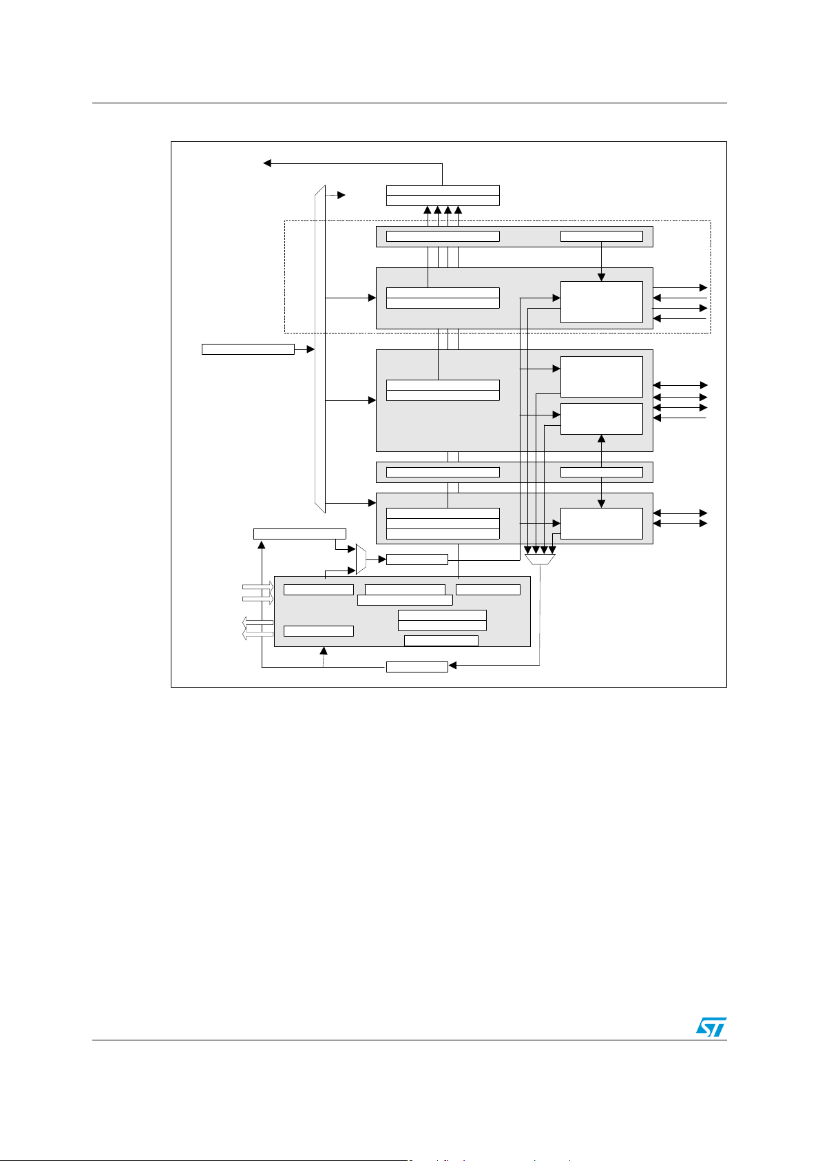
Serial interfaces STM32W108C8
SC1_UARTSTAT
SCx_SPISTAT
SCx_SPICFG
SCx_I2CSTAT
SCx_I2CCTRL1
SCx_I2CCTRL2
SCx_RATELIN/EXP
SC1_UARTPER/FRAC Baud Generator
Clock Generator
UART
Controller
I2C Master
Controller
SCx_DATA
SPI Master
Controller
UART
SPI
I
2
C
OFF
SCx_MODE
0
1
2
3
nRTS
nCTS
SCLK
MOSI
MISO
SDA
TXD
RXD
RX-FIFO
TX-FIFO
SCx_TX/RXBEGA/B
SCx_RXCNTA/B SCx_TXCNT
SCx_DMASTAT
SCx_DMACTRL
SCx_RXERRA/B
DMA
Controller
SCL
INT_SCxFLAG
INT_SCxCFG
SC1_UARTCFG
SCx Interrupt
SCx TX DMA
channel
SCx RX DMA
channel
SCx_TX/RXENDA/B
SPI Slave
Controller
nSSEL
SCx_RXCNTSAVED
SC1
only
Figure 8. Serial controller block diagram
9.2 Configuration
73/215 Doc ID 018587 Rev 2
Before using a serial controller, it should be configured and initialized as follows:
1. Set up the parameters specific to the operating mode (master/slave for SPI, baud rate
for UART, etc.).
2. Configure the GPIO pins used by the serial controller as shown in Ta bl e 3 9 and
Ta bl e 4 0. Section 8.1.2: Configuration on page 56 shows how to configure GPIO
pins."If using DMA, set up the DMA and buffers. This is described fully in Section 9.13:
DMA channel registers on page 100.
3. If using interrupts, select edge- or level-triggered interrupts with the SCx_INTMODE
register, enable the desired second-level interrupt sources in the INT_SCxCFG
register, and finally enable the top-level SCx interrupt in the NVIC.
4. Write the serial interface operating mode - SPI, I
register.
2
C, or UART - to the SCx_MODE
Page 75

STM32W108C8 Serial interfaces
Table 39. SC1 GPIO usage and configuration
Interface PB1 PB2 PB3 PB4
SPI - Master
SPI - Slave
2
C - Master
I
UART
1. used if RTS/CTS hardware flow control is enabled.
Table 40. SC2 GPIO usage and configuration
SC1MOSI alternate
output (push-pull)
SC1MISO alternate
output (push-pull)
SC1SDA alternate
output (open-drain)
TXD alternate
output (push-pull)
SC1MISO input
SC1MOSI input SC1SCLK input SC1nSSEL input
SC1SCL alternate
output (open-drain)
RXD input nCTS input
SC1SCLK alternate
output (push-pull);
(not used)
special SCLK mode
(not used) (not used)
(1)
nRTS alternate
output (push-pull)
(1)
Interface PA0 PA1 PA2 PA3
SC2SCLK
Alternate Output
(push-pull), special
SCLK mode
(not used)
SPI - Master
SC2MOSI
Alternate Output
(push-pull)
SC2MISO Input
SC2MOSI
SPI - Slave
Alternate Output
SC2MISO Input SC2SCLK Input SC2nSSEL Input
(push-pull)
2
C - Master (not used)
I
SC2SDA Alternate
Output (open-drain)
SC2SCL Alternate
Output (open-drain)
(not used)
9.3 SPI master mode
The SPI master controller has the following features:
● Full duplex operation
● Programmable clock frequency (6 MHz max.)
● Programmable clock polarity and phase
● Selectable data shift direction (either LSB or MSB first)
● Receive and transmit FIFOs
● Receive and transmit DMA channels
The SPI master controller uses the three signals:
● MOSI (Master Out, Slave In) - outputs serial data from the master
● MISO (Master In, Slave Out) - inputs serial data from a slave
● SCLK (Serial Clock) - outputs the serial clock used by MOSI and MISO
The GPIO pins used for these signals are shown in Ta b le 4 1 . Additional outputs may be
needed to drive the nSSEL signals on slave devices.
Doc ID 018587 Rev 2 74/215
Page 76

Serial interfaces STM32W108C8
Rate
12MHz
LIN 1+()x2
EXP
-----------------------------------------=
SCLK
out
MOSI
out
MISO
in
RX[7]
TX[7]
RX[6]
TX[6 ]
RX[5]
TX[ 5]
RX[4]
TX[4]
RX[3]
TX[3 ]
RX[2]
TX[2 ]
RX[1]
TX[ 1]
RX[0]
TX[0]
MOSI
out
MISO
in
RX[7]
TX[7]
RX[6]
TX[6 ]
RX[5]
TX[5]
RX[4]
TX[4]
RX[3]
TX[3 ]
RX[2]
TX[ 2]
RX[1]
TX[1]
RX[0]
TX[0 ]
SCLK
out
Table 41. SPI master GPIO usage
Parameter MOSI MISO SCLK
Direction Output Input Output
GPIO
configuration
Alternate Output
(push-pull)
Input
Alternate Output (push-pull)
Special SCLK mode
SC1 pin PB1 PB2 PB3
SC2 pin PA0 PA1 PA2
9.3.1 Setup and configuration
Both serial controllers, SC1 and SC2, support SPI master mode. SPI master mode is
enabled by the following register settings:
● The serial controller mode register (SCx_MODE) is ‘2’.
● The SC_SPIMST bit in the SPI configuration register (SCx_SPICFG) is ‘1’.
● The SC_TWIACK bit in the I
The SPI serial clock (SCLK) is produced by a programmable clock generator. The serial
clock is produced by dividing down 12 MHz according to this equation:
2
C control register (SCx_TWICTRL2) is ‘1’.
EXP is the value written to the SCx_RATEEXP register and LIN is the value written to the
SCx_RATELIN register. The SPI master mode clock may not exceed 6 Mbps, so EXP and
LIN cannot both be zero.
The SPI master controller supports various frame formats depending upon the clock polarity
(SC_SPIPOL), clock phase (SC_SPIPHA), and direction of data (SC_SPIORD) (see SPI
master mode formats on page 75). The bits SC_SPIPOL, SC_SPIPHA, and SC_SPIORD
are defined within the SCx_SPICFG register.
Table 42. SPI master mode formats
MST ORD PHA POL
1000
1001
SCx_SPICFG
(1)
Frame formatsSC_SPIxxx
75/215 Doc ID 018587 Rev 2
Page 77

STM32W108C8 Serial interfaces
MOSI
out
MISO
in
RX[7]
TX[7 ]
RX[6]
TX[6]
RX[5]
TX[5]
RX[4]
TX[4 ]
RX[3]
TX[3]
RX[2]
TX[2]
RX[1]
TX[1 ]
RX[0]
TX [0]
SCL K
out
MOSI
out
MISO
in
RX[7]
TX[7]
RX[6]
TX[6 ]
RX[5]
TX[5]
RX[4]
TX[4]
RX[3]
TX [3]
RX[2]
TX[2]
RX[1]
TX[1]
RX[0]
TX[0 ]
SCLK
out
Table 42. SPI master mode formats (continued)
SCx_SPICFG
(1)
Frame formatsSC_SPIxxx
MST ORD PHA POL
1010
1011
1 1 - - Same as above except data is sent LSB first instead of MSB first.
1. The notation xxx means that the corresponding column header below is inserted to form the field name.
9.3.2 Operation
Characters transmitted and received by the SPI master controller are buffered in transmit
and receive FIFOs that are both 4 entries deep. When software writes a character to the
SCx_DATA register, the character is pushed onto the transmit FIFO. Similarly, when
software reads from the SCx_DATA register, the character returned is pulled from the
receive FIFO. If the transmit and receive DMA channels are used, they also write to and
read from the transmit and receive FIFOs.
When the transmit FIFO and the serializer are both empty, writing a character to the transmit
FIFO clears the SC_SPITXIDLE bit in the SCx_SPISTAT register. This indicates that some
characters have not yet been transmitted. If characters are written to the transmit FIFO until
it is full, the SC_SPITXFREE bit in the SCx_SPISTAT register is cleared. Shifting out a
character to the MOSI pin sets the SC_SPITXFREE bit in the SCx_SPISTAT register. When
the transmit FIFO empties and the last character has been shifted out, the SC_SPITXIDLE
bit in the SCx_SPISTAT register is set.
Characters received are stored in the receive FIFO. Receiving characters sets the
SC_SPIRXVAL bit in the SCx_SPISTAT register, indicating that characters can be read from
the receive FIFO. Characters received while the receive FIFO is full are dropped, and the
SC_SPIRXOVF bit in the SCx_SPISTAT register is set. The receive FIFO hardware
generates the INT_SCRXOVF interrupt, but the DMA register will not indicate the error
condition until the receive FIFO is drained. Once the DMA marks a receive error, two
conditions will clear the error indication: setting the appropriate SC_TX/RXDMARST bit in
the SCx_DMACTRL register, or loading the appropriate DMA buffer after it has unloaded.
To receive a character, you must transmit a character. If a long stream of receive characters
is expected, a long sequence of dummy transmit characters must be generated. To avoid
software or transmit DMA initiating these transfers and consuming unnecessary bandwidth,
the SPI serializer can be instructed to retransmit the last transmitted character or to transmit
a busy token (0xFF), which is determined by the SC_SPIRPT bit in the SCx_SPICFG
register. This functionality can only be enabled or disabled when the transmit FIFO is empty
and the transmit serializer is idle, indicated by a cleared SC_SPITXIDLE bit in the
SCx_SPISTAT register.
Doc ID 018587 Rev 2 76/215
Page 78

Serial interfaces STM32W108C8
Every time an automatic character transmission starts, a transmit underrun is detected as
there is no data in transmit FIFO, and the INT_SCTXUND bit in the INT_SC2FLAG register
is set. After automatic character transmission is disabled, no more new characters are
received. The receive FIFO holds characters just received.
Note: The Receive DMA complete event does not always mean the receive FIFO is empty.
The DMA Channels section describes how to configure and use the serial receive and
transmit DMA channels.
9.3.3 Interrupts
SPI master controller second level interrupts are generated by the following events:
● Transmit FIFO empty and last character shifted out (depending on SCx_INTMODE,
either the 0 to 1 transition or the high level of SC_SPITXIDLE)
● Transmit FIFO changed from full to not full (depending on SCx_INTMODE, either the 0
to 1 transition or the high level of SC_SPITXFREE)
● Receive FIFO changed from empty to not empty (depending on SCx_INTMODE, either
the 0 to 1 transition or the high level of SC_SPIRXVAL)
● Transmit DMA buffer A/B complete (1 to 0 transition of SC_TXACTA/B)
● Receive DMA buffer A/B complete (1 to 0 transition of SC_RXACTA/B)
● Received and lost character while receive FIFO was full (receive overrun error)
● Transmitted character while transmit FIFO was empty (transmit underrun error)
To enable CPU interrupts, set the desired interrupt bits in the second level INT_SCxCFG
register, and enable the top level SCx interrupt in the NVIC by writing the INT_SCx bit in the
INT_CFGSET register.
9.4 SPI slave mode
Both SC1 and SC2 SPI controllers include a SPI slave controller with these features:
● Full duplex operation
● Up to 5 Mbps data transfer rate
● Programmable clock polarity and clock phase
● Selectable data shift direction (either LSB or MSB first)
● Slave select input
The SPI slave controller uses four signals:
● MOSI (Master Out, Slave In) - inputs serial data from the master
● MISO (Master In, Slave Out) - outputs serial data to the master
● SCLK (Serial Clock) - clocks data transfers on MOSI and MISO
● nSSEL (Slave Select) - enables serial communication with the slave
The GPIO pins that can be assigned to these signals are shown in Ta bl e 4 3.
77/215 Doc ID 018587 Rev 2
Page 79

STM32W108C8 Serial interfaces
TX[7]
RX[7]
TX[6]
RX[6]
TX [5]
RX[5]
TX[4]
RX[4]
TX[3]
RX[3]
TX[2]
RX[2]
TX[1 ]
RX[1]
TX[ 0]
RX[0]
nSSEL
SCLK
in
MOSI
in
MISO
out
TX[7]
RX[7]
TX[6]
RX[6]
TX[5 ]
RX[5]
TX[4]
RX[4]
TX[3]
RX[3]
TX[2 ]
RX[2]
TX[ 1]
RX[1]
TX[0]
RX[0]
SCLK
in
MOSI
in
MISO
out
TX[7]
RX[7]
TX[6]
RX[6]
TX[5 ]
RX[5]
TX[4]
RX[4]
TX[3]
RX[3]
TX [2]
RX[2]
TX[1]
RX[1]
TX[0]
RX[0]
nSSE L
SCLK
in
MOSI
in
MISO
out
Table 43. SPI slave GPIO usage
Parameter MOSI MISO SCLK nSSEL
Direction Input Output Input Input
GPIO
configuration
Input
Alternate Output
(push-pull)
Input Input
SC1 pin PB2 PB1 PB3 PB4
SC2 pin PA0 PA1 PA2 PA3
9.4.1 Setup and configuration
Both serial controllers, SC1 and SC2, support SPI slave mode. SPI slave mode is enabled
by the following register settings:
● The serial controller mode register, SCx_MODE, is ‘2’.
● The SC_SPIMST bit in the SPI configuration register, SCx_SPICFG, is ‘0’.
The SPI slave controller receives its clock from an external SPI master device and supports
rates up to 5 Mbps.
The SPI slave controller supports various frame formats depending upon the clock polarity
(SC_SPIPOL), clock phase (SC_SPIPHA), and direction of data (SC_SPIORD) (see Table 8
6). The SC_SPIPOL, SC_SPIPHA, and SC_SPIORD bits are defined within the
SCx_SPICFG registers.
Table 44. SPI slave mode formats
SCx_SPICFG
(1)
MST ORD PHA POL
0000
0001
0010
Frame formatSC_SPIxxx
Doc ID 018587 Rev 2 78/215
Page 80

Serial interfaces STM32W108C8
TX[ 7]
RX[7]
TX[6]
RX[6]
TX[5 ]
RX[5]
TX[4]
RX[4]
TX[3]
RX[3]
TX[2 ]
RX[2]
TX[ 1]
RX[1]
TX[0]
RX[0]
nSSEL
MOSI
in
MISO
out
SCLK
in
Table 44. SPI slave mode formats (continued)
SCx_SPICFG
(1)
Frame formatSC_SPIxxx
MST ORD PHA POL
0011
0 1 - - Same as above except LSB first instead of MSB first.
1. The notation xxx means that the corresponding column header below is inserted to form the field name.
9.4.2 Operation
When the slave select (nSSEL) signal is asserted by the master, SPI transmit data is driven
to the output pin MISO, and SPI data is received from the input pin MOSI. The nSSEL pin
has to be asserted to enable the transmit serializer to drive data to the output signal MISO.
A falling edge on nSSEL resets the SPI slave shift registers.
Characters transmitted and received by the SPI slave controller are buffered in the transmit
and receive FIFOs that are both 4 entries deep. When software writes a character to the
SCx_DATA register, it is pushed onto the transmit FIFO. Similarly, when software reads from
the SCx_DATA register, the character returned is pulled from the receive FIFO. If the
transmit and receive DMA channels are used, the DMA channels also write to and read from
the transmit and receive FIFOs.
Characters received are stored in the receive FIFO. Receiving characters sets the
SC_SPIRXVAL bit in the SCx_SPISTAT register, to indicate that characters can be read
from the receive FIFO. Characters received while the receive FIFO is full are dropped, and
the SC_SPIRXOVF bit in the SCx_SPISTAT register is set. The receive FIFO hardware
generates the INT_SCRXOVF interrupt, but the DMA register will not indicate the error
condition until the receive FIFO is drained. Once the DMA marks a receive error, two
conditions will clear the error indication: setting the appropriate SC_TX/RXDMARST bit in
the SCx_DMACTRL register, or loading the appropriate DMA buffer after it has unloaded.
Receiving a character causes the serial transmission of a character pulled from the transmit
FIFO. When the transmit FIFO is empty, a transmit underrun is detected (no data in transmit
FIFO) and the INT_SCTXUND bit in the INT_SCxFLAG register is set. Because no
character is available for serialization, the SPI serializer retransmits the last transmitted
character or a busy token (0xFF), determined by the SC_SPIRPT bit in the SCx_SPICFG
register.
When the transmit FIFO and the serializer are both empty, writing a character to the transmit
FIFO clears the SC_SPITXIDLE bit in the SCx_SPISTAT register. This indicates that not all
characters have been transmitted. If characters are written to the transmit FIFO until it is full,
the SC_SPITXFREE bit in the SCx_SPISTAT register is cleared. Shifting out a transmit
character to the MISO pin causes the SC_SPITXFREE bit in the SCx_SPISTAT register to
get set. When the transmit FIFO empties and the last character has been shifted out, the
SC_SPITXIDLE bit in the SCx_SPISTAT register is set.
79/215 Doc ID 018587 Rev 2
Page 81

STM32W108C8 Serial interfaces
The SPI slave controller must guarantee that there is time to move new transmit data from
the transmit FIFO into the hardware serializer. To provide sufficient time, the SPI slave
controller inserts a byte of padding at the start of every new string of transmit data. After
slave select asserts and the SC_SPIRXVAL bit in the SCx_SPISTAT register gets set at
least once, the following operation holds true until slave select deasserts. Whenever the
transmit FIFO is empty and data is placed into the transmit FIFO, either manually or through
DMA, the SPI hardware inserts a byte of padding onto the front of the transmission as if this
byte was placed there by software. The value of the byte of padding that is inserted is
selected by the SC_SPIRPT bit in the SCx_SPICFG register.
9.4.3 DMA
The DMA Channels section describes how to configure and use the serial receive and
transmit DMA channels.
When using the receive DMA channel and nSSEL transitions to the high (deasserted) state,
the active buffer's receive DMA count register (SCx_RXCNTA/B) is saved in the
SCx_RXCNTSAVED register. SCx_RXCNTSAVED is only written the first time nSSEL goes
high after a buffer has been loaded. Subsequent rising edges set a status bit but are
otherwise ignored. The 3-bit field SC_RXSSEL in the SCx_DMASTAT register records what,
if anything, was saved to the SCx_RXCNTSAVED register, and whether or not another
rising edge occurred on nSSEL.
9.4.4 Interrupts
SPI slave controller second level interrupts are generated on the following events:
● Transmit FIFO empty and last character shifted out (depending on SCx_INTMODE,
either the 0 to 1 transition or the high level of SC_SPITXIDLE)
● Transmit FIFO changed from full to not full (depending on SCx_INTMODE, either the 0
to 1 transition or the high level of SC_SPITXFREE)
● Receive FIFO changed from empty to not empty (depending on SCx_INTMODE, either
the 0 to 1 transition or the high level of SC_SPIRXVAL)
● Transmit DMA buffer A/B complete (1 to 0 transition of SC_TXACTA/B)
● Receive DMA buffer A/B complete (1 to 0 transition of SC_RXACTA/B)
● Received and lost character while receive FIFO was full (receive overrun error)
● Transmitted character while transmit FIFO was empty (transmit underrun error)
To enable CPU interrupts, set desired interrupt bits in the second level INT_SCxCFG
register, and also enable the top level SCx interrupt in the NVIC by writing the INT_SCx bit
in the INT_CFGSET register.
9.5 Inter-integrated circuit interfaces (I2C)
Both STM32W108C8 serial controllers SC1 and SC2 include an Inter-integrated circuit
interface (I
● Uses only two bidirectional GPIO pins
● Programmable clock frequency (up to 400 kHz)
● Supports both 7-bit and 10-bit addressing
● Compatible with Philips' I
2
C) master controller with the following features:
2
C-bus slave devices
Doc ID 018587 Rev 2 80/215
Page 82

Serial interfaces STM32W108C8
Rate
12MHz
LIN 1+()x2
EXP
-----------------------------------------=
The I2C master controller uses just two signals:
● SDA (Serial Data) - bidirectional serial data
● SCL (Serial Clock) - bidirectional serial clock
Ta bl e 4 5 lists the GPIO pins used by the SC1 and SC2 I
2
C master controllers. Because the
pins are configured as open-drain outputs, they require external pull-up resistors.
Table 45. I
Direction Input / Output Input / Output
2
C Master GPIO Usage
Parameter SDA SCL
GPIO configuration
SC1 pin PB1 PB2
SC2 pin PA1 PA2
9.5.1 Setup and configuration
The I2C controller is enabled by writing 3 to the SCx_MODE register. The I2C controller
operates only in master mode and supports both Standard (100 kbps) and Fast (400 kbps)
2
I
C modes. Address arbitration is not implemented, so multiple master applications are not
supported.
2
The I
C master controller's serial clock (SCL) is produced by a programmable clock
generator. SCL is produced by dividing down 12 MHz according to this equation:
EXP is the value written to the SCx_RATEEXP register and LIN is the value written to the
SCx_RATELIN register. I2C clock rate programming on page 81 shows the rate settings for
Standard-Mode I
Table 46. I2C clock rate programming
2
C (100 kbps) and Fast-Mode I2C (400 kbps) operation.
Clock rate SCx_RATELIN SCx_RATEEXP
Alternate Output
(open drain)
Alternate Output
(open drain)
100 kbps 14 3
375 kbps 15 1
400 kbps 14 1
Note: At 400 kbps, the Philips I2C Bus specification requires the minimum low period of SCL to be
1.3 µs, but on the STM32W108 it is 1.25 µs. If a slave device requires strict compliance with
SCL timing, the clock rate must be lowered to 375 kbps.
9.5.2 Constructing frames
The I2C master controller supports generating various frame segments by means of the
SC_TWISTART, SC_TWISTOP, SC_TWISEND, and SC_TWIRECV bits in the
SCx_TWICTRL1 registers. Figure 47 summarizes these frames.
81/215 Doc ID 018587 Rev 2
Page 83

STM32W108C8 Serial interfaces
TWI re-s tart segment - after transmit or fram e wit h NA CK
SDA
out
SDA
outSLAVE
SCL
outSLAVE
SCL
out
TWI st art s egment
SDA
out
SDA
outSLAVE
SCL
outSLAVE
SCL
out
SCL
out
TX[7]TX[6]TX[5]TX[4]TX[3]TX[2]TX[1]TX[0]
SDA
out
SDA
outSLAVE
SCL
outSLAVE
(N)ACK
TWI transmit segment - after (re-)start frame
SCL
out
TX[7]TX[6]TX[5]TX[4]TX[3]TX[2]TX[1]TX[0]
SDA
out
SDA
outSLAVE
SCL
outSLAVE
(N)ACK
TWI transmit segment – after transmit with ACK
SCL
out
RX[7]RX[6]RX[5]RX[4]RX[3]RX[2]RX[1]RX[0]
SDA
out
SDA
outSLAVE
SCL
outSLAVE
(N)ACK
TWI receive segment – transmit with ACK
SCL
out
RX[7]RX[6]RX[5]RX[4]RX[3]RX[2]RX[1]RX[0]
SDA
out
SDA
outSLAVE
SCL
outSLAVE
(N)ACK
TWI rec eiv e segm ent - after rec eive wit h AC K
TWI stop segm ent - after f rame with NA CK or stop
SDA
out
SDA
outSLAVE
SCL
outSLAVE
SCL
out
Table 47. I
2
C master frame segments
SCx_TWICTRL1
(1)
START SEND RECV STOP
1000
0100
Frame segmentsSC_TWIxxxx
0010
0001
0 0 0 0 No pending frame segment
1
-
-
1
1. The notation xxx means that the corresponding column header below is inserted to form the field name.
1
1
-
-
Full I2C frames have to be constructed by software from individual I2C segments. All
necessary segment transitions are shown in Figure 9. ACK or NACK generation of an I
1
1
-
-
Illegal
1
1
2
C
Doc ID 018587 Rev 2 82/215
Page 84

Serial interfaces STM32W108C8
RECEIVE Segment
with NACK
RECEIVE Segment
with ACK
IDLE
START Segment
STOP Segment TRANSMIT Segment
received ACK ?
NO
YES
receive frame segment is determined with the SC_TWIACK bit in the SCx_TWICTRL2
register.
Figure 9. I
2
C segment transitions
Generation of a 7-bit address is accomplished with one transmit segment. The upper 7 bits
of the transmitted character contain the 7-bit address. The remaining lower bit contains the
command type ("read" or "write").
Generation of a 10-bit address is accomplished with two transmit segments. The upper 5
bits of the first transmit character must be set to 0x1E. The next 2 bits are for the 2 most
significant bits of the 10-bit address. The remaining lower bit contains the command type
("read" or "write"). The second transmit segment is for the remaining 8 bits of the 10-bit
address.
Transmitted and received characters are accessed through the SCx_DATA register.
To initiate (re)start and stop segments, set the SC_TWISTART or SC_TWISTOP bit in the
SCx_TWICTRL1 register, then wait until the bit is clear. Alternatively, the SC_TWICMDFIN
bit in the SCx_TWISTAT can be used for waiting.
To initiate a transmit segment, write the data to the SCx_DATA data register, then set the
SC_TWISEND bit in the SCx_TWICTRL1 register, and finally wait until the bit is clear.
Alternatively the SC_TWITXFIN bit in the SCx_TWISTAT register can be used for waiting.
To initiate a receive segment, set the SC_TWIRECV bit in the SCx_TWICTRL1 register, wait
until it is clear, and then read from the SCx_DATA register. Alternatively, the SC_TWIRXFIN
bit in the SCx_TWISTAT register can be used for waiting. Now the SC_TWIRXNAK bit in the
SCx_TWISTAT register indicates if a NACK or ACK was received from an I
2
C slave device.
83/215 Doc ID 018587 Rev 2
Page 85

STM32W108C8 Serial interfaces
9.5.3 Interrupts
I2C master controller interrupts are generated on the following events:
● Bus command (SC_TWISTART/SC_TWISTOP) completed (0 to 1 transition of
SC_TWICMDFIN)
● Character transmitted and slave device responded with NACK
● Character transmitted (0 to 1 transition of SC_TWITXFIN)
● Character received (0 to 1 transition of SC_TWIRXFIN)
● Received and lost character while receive FIFO was full (receive overrun error)
● Transmitted character while transmit FIFO was empty (transmit underrun error)
To enable CPU interrupts, set the desired interrupt bits in the second level INT_SCxCFG
register, and enable the top level SCx interrupt in the NVIC by writing the INT_SCx bit in the
INT_CFGSET register.
9.6 Universal asynchronous receiver / transmitter (UART)
The SC1 UART is enabled by writing 1 to SC1_MODE. The SC2 serial controller does not
include UART functions.
The UART supports the following features:
● Flexible baud rate clock (300 bps to 921.6 bps)
● Data bits (7 or 8)
● Parity bits (none, odd, or even)
● Stop bits (1 or 2)
● False start bit and noise filtering
● Receive and transmit FIFOs
● Optional RTS/CTS flow control
● Receive and transmit DMA channels
The UART uses two signals to transmit and receive serial data:
● TXD (Transmitted Data) - serial data received by the STM32W108C8
● RXD (Received Data) - serial data sent by the STM32W108C8
If RTS/CTS flow control is enabled, these two signals are also used:
● nRTS (Request To Send) - indicates the STM32W108C8 is able to receive data RXD
● nCTS (Clear To Send) - inhibits sending data from the STM32W108C8 if not asserted
The GPIO pins assigned to these signals are shown in Ta bl e 4 8 .
Table 48. UART GPIO usage
Parameter TXD RXD nCTS
(1)
Direction Output Input Input Output
GPIO configuration
Alternate Output
(push-pull)
Input Input
Alternate Output
SC1 pin PB1 PB2 PB3 PB4
1. Only used if RTS/CTS hardware flow control is enabled.
Doc ID 018587 Rev 2 84/215
(1)
nRTS
(push-pull)
Page 86

Serial interfaces STM32W108C8
FN
MHz
baud+=
2
24
9.6.1 Setup and configuration
The UART baud rate clock is produced by a programmable baud generator starting from the
24 Hz clock:
The integer portion of the divisor, N, is written to the SC1_UARTPER register and the
fractional part, F, to the SC1_UARTFRAC register. Tab l e 4 9 shows the values used to
generate some common baud rates and their associated clock frequency error. The UART
requires an internal clock that is at least eight times the baud rate clock, so the minimum
allowable setting for SC1_UARTPER is ‘8’.
Table 49. UART baud rate divisors for common baud rates
Baud rate (bits/sec) SC1_UARTPER SC1_UARTFRAC Baud rate error (%)
300 40000 0 0
2400 5000 0 0
4800 2500 0 0
9600 1250 0 0
19200 625 0 0
38400 312 1 0
57600 208 1 - 0.08
115200 104 0 + 0.16
230400 52 0 + 0.16
460800 26 0 + 0.16
921600 13 0 + 0.16
Note: The UART may receive corrupt bytes if the interbyte gap is long or there is a baud rate
mismatch between receive and transmit. The UART may detect a parity and/or framing error
on the corrupt byte, but there will not necessarily be any error detected. As a result, the
device should be operated in systems where the other side of the communication link also
uses a crystal as its timing reference, and baud rates should be selected to minimize the
baud rate mismatch to the crystal tolerance. UART protocols should contain some form of
error checking (e.g. CRC) at the packet level to detect, and retry in the event of errors.
The UART character frame format is determined by three bits in the SC1_UARTCFG
register:
● SC1_UART2STP selects the number of stop bits in transmitted characters. (Only one
stop bit is ever required in received characters.) If this bit is clear, characters are
transmitted with one stop bit; if set, characters are transmitted with two stop bits.
● SC1_UARTPAR controls whether or not received and transmitted characters include a
parity bit. If SC1_UARTPAR is clear, characters do not contain a parity bit, otherwise,
characters do contain a parity bit.
● SC1_UARTODD specifies whether transmitted and received parity bits contain odd or
even parity. If this bit is clear, the parity bit is even, and if set, the parity bit is odd. Even
parity is the exclusive-or of all of the data bits, and odd parity is the inverse of the even
parity value. SC1_UARTODD has no effect if SC1_UARTPAR is clear.
85/215 Doc ID 018587 Rev 2
Page 87

STM32W108C8 Serial interfaces
Idle tim e
Start
Bit
Data
Bit 0
Data
Bit 1
Data
Bit 2
Data
Bit 3
Data
Bit 4
Data
Bit 5
Data
Bit 6
Data
Bit 7
Pari ty
Bit
Stop
Bit
Stop
Bit
Next
Start Bi t
or
IdleTim e
UAR T Char acter Fram e Form at
(opt ional s ecti ons are i n itali cs )
TXD
or
RXD
Receive Shift Register
SC1_DATA (read)
Transmit Shift Register
SC1_D ATA (wr ite)
RXD
TXD
Parity/Frame Errors
SC1_UARTSTAT
Rece ive FIF O
Transmit F IFO
CPU and DMA
Channel Access
A UART character frame contains, in sequence:
● The start bit
● The least significant data bit
● The remaining data bits
● If parity is enabled, the parity bit
● The stop bit, or bits, if 2 stop bits are selected.
Figure 10 shows the UART character frame format, with optional bits indicated. Depending
on the options chosen for the character frame, the length of a character frame ranges from 9
to 12 bit times.
Note that asynchronous serial data may have arbitrarily long idle periods between
characters. When idle, serial data (TXD or RXD) is held in the high state. Serial data
transitions to the low state in the start bit at the beginning of a character frame.
Figure 10. UART character frame format
9.6.2 FIFOs
Characters transmitted and received by the UART are buffered in the transmit and receive
FIFOs that are both 4 entries deep (see Figure 11). When software writes a character to the
SC1_DATA register, it is pushed onto the transmit FIFO. Similarly, when software reads from
the SC1_DATA register, the character returned is pulled from the receive FIFO. If the
transmit and receive DMA channels are used, the DMA channels also write to and read from
the transmit and receive FIFOs.
Figure 11. UART FIFOs
9.6.3 RTS/CTS flow control
RTS/CTS flow control, also called hardware flow control, uses two signals (nRTS and nCTS)
in addition to received and transmitted data (see Figure 12). Flow control is used by a data
receiver to prevent buffer overflow, by signaling an external device when it is and is not
allowed to transmit.
Doc ID 018587 Rev 2 86/215
Page 88

Serial interfaces STM32W108C8
Other Device
UART Receiver
UART Transmitter
STM32W108
UART Transmitter
UART Receiver
RXD TXD
nRTS nCTS
TXD RXD
nCTS nRTS
Figure 12. RTS/CTS flow control connections
The UART RTS/CTS flow control options are selected by the SC1_UARTFLOW and
SC1_UARTAUTO bits in the SC1_UARTCFG register (see Tab le 5 0). Whenever the
SC1_UARTFLOW bit is set, the UART will not start transmitting a character unless nCTS is
low (asserted). If nCTS transitions to the high state (deasserts) while a character is being
transmitted, transmission of that character continues until it is complete.
If the SC1_UARTAUTO bit is set, nRTS is controlled automatically by hardware: nRTS is put
into the low state (asserted) when the receive FIFO has room for at least two characters,
otherwise is it in the high state (unasserted). If SC1_UARTAUTO is clear, software controls
the nRTS output by setting or clearing the SC1_UARTRTS bit int the SC1_UARTCFG
register. Software control of nRTS is useful if the external serial device cannot stop
transmitting characters promptly when nRTS is set to the high state (deasserted).
Table 50. UART RTS/CTS flow control configurations
SC1_UARTCFG
(1)
FLOW AUTO RTS
0 - - TXD, RXD No RTS/CTS flow control
100/1
11-
1. The notation xxx means that the corresponding column header below is inserted to form the field name.
Pins used Operating modeSC1_UARTxxx
TX D, RXD,
nCTS, nRTS
TX D, RXD,
nCTS, nRTS
Flow control using RTS/CTS with software control of nRTS:
nRTS controlled by SC1_UARTRTS bit in SC1_UARTCFG register
Flow control using RTS/CTS with hardware control of nRTS:
nRTS is asserted if room for at least 2 characters in receive FIFO
9.6.4 DMA
The DMA Channels section describes how to configure and use the serial receive and
transmit DMA channels.
The receive DMA channel has special provisions to record UART receive errors. When the
DMA channel transfers a character from the receive FIFO to a buffer in memory, it checks
the stored parity and frame error status flags. When an error is flagged, the
SC1_RXERRA/B register is updated, marking the offset to the first received character with a
parity or frame error. Similarly if a receive overrun error occurs, the SC1_RXERRA/B
registers mark the error offset. The receive FIFO hardware generates the INT_SCRXOVF
interrupt and DMA status register indicates the error immediately, but in this case the error
87/215 Doc ID 018587 Rev 2
Page 89

STM32W108C8 Serial interfaces
offset is 4 characters ahead of the actual overflow at the input to the receive FIFO. Two
conditions will clear the error indication: setting the appropriate SC_RXDMARST bit in the
SC1_DMACTRL register, or loading the appropriate DMA buffer after it has unloaded.
9.6.5 Interrupts
UART interrupts are generated on the following events:
● Transmit FIFO empty and last character shifted out (depending on SCx_INTMODE,
either the 0 to 1 transition or the high level of SC1_UARTTXIDLE)
● Transmit FIFO changed from full to not full (depending on SCx_INTMODE, either the 0
to 1 transition or the high level of SC1_UARTTXFREE)
● Receive FIFO changed from empty to not empty (depending on SCx_INTMODE, either
the 0 to 1 transition or the high level of SC1_UARTRXVAL)
● Transmit DMA buffer A/B complete (1 to 0 transition of SC_TXACTA/B)
● Receive DMA buffer A/B complete (1 to 0 transition of SC_RXACTA/B)
● Character received with parity error
● Character received with frame error
● Character received and lost when receive FIFO was full (receive overrun error)
To enable CPU interrupts, set the desired interrupt bits in the second level INT_SCxCFG
register, and enable the top level SCx interrupt in the NVIC by writing the INT_SCx bit in the
INT_CFGSET register.
9.7 Direct memory access (DMA) channels
The STM32W108C8 serial DMA channels enable efficient, high-speed operation of the SPI
and UART controllers by reducing the load on the CPU as well as decreasing the frequency
of interrupts that it must service. The transmit and receive DMA channels can transfer data
between the transmit and receive FIFOs and the DMA buffers in main memory as quickly as
it can be transmitted or received. Once software defines, configures, and activates the DMA,
it only needs to handle an interrupt when a transmit buffer has been emptied or a receive
buffer has been filled. The DMA channels each support two memory buffers, labeled A and
B, and can alternate ("ping-pong") between them automatically to allow continuous
communication without critical interrupt timing.
Note: DMA memory buffer terminology:
●
load - make a buffer available for the DMA channel to use
●
pending - a buffer loaded but not yet active
●
active - the buffer that will be used for the next DMA transfer
●
unload - DMA channel action when it has finished with a buffer
●
idle - a buffer that has not been loaded, or has been unloaded
To use a DMA channel, software should follow these steps:
● Reset the DMA channel by setting the SC_TXDMARST (or SC_RXDMARST) bit in the
SCx_DMACTRL register.
● Set up the DMA buffers. The two DMA buffers, A and B, are defined by writing the start
address to SCx_TXBEGA/B (or SCx_RXBEGA/B) and the (inclusive) end address to
SCx_TXENDA/B (or SCx_RXENDA/B). Note that DMA buffers must be in RAM.
● Configure and initialize SCx for the desired operating mode.
● Enable second level interrupts triggered when DMA buffers unload by setting the
INT_SCTXULDA/B (or INT_SCRXULDA/B) bits in the INT_SCxFLAG register.
Doc ID 018587 Rev 2 88/215
Page 90

Serial interfaces STM32W108C8
● Enable top level NVIC interrupts by setting the INT_SCx bit in the INT_CFGSET
register.
● Start the DMA by loading the DMA buffers by setting the SC_TXLODA/B (or
SC_RXLODA/B) bits in the SCx_DMACTRL register.
A DMA buffer's end address, SCx_TXENDA/B (or SCx_RXENDA/B), can be written while
the buffer is loaded or active. This is useful for receiving messages that contain an initial
byte count, since it allows software to set the buffer end address at the last byte of the
message.
As the DMA channel transfers data between the transmit or receive FIFO and a memory
buffer, the DMA count register contains the byte offset from the start of the buffer to the
address of the next byte that will be written or read. A transmit DMA channel has a single
DMA count register (SCx_TXCNT) that applies to whichever transmit buffer is active, but a
receive DMA channel has two DMA count registers (SCx_RXCNTA/B), one for each receive
buffer. The DMA count register contents are preserved until the corresponding buffer, or
either buffer in the case of the transmit DMA count, is loaded, or until the DMA is reset.
The receive DMA count register may be written while the corresponding buffer is loaded. If
the buffer is not loaded, writing the DMA count register also loads the buffer while
preserving the count value written. This feature can simplify handling UART receive errors.
The DMA channel stops using a buffer and unloads it when the following is true:
(DMA buffer start address + DMA buffer count) > DMA buffer end address
Typically a transmit buffer is unloaded after all its data has been sent, and a receive buffer is
unloaded after it is filled with data, but writing to the buffer end address or buffer count
registers can also cause a buffer to unload early.
Serial controller DMA channels include additional features specific to the SPI and UART
operation and are described in those sections.
9.8 Serial controller registers
9.8.1 Serial mode register (SCx_MODE)
Address offset: 0xC854 (SC1_MODE) and 0xC054 (SC2_MODE)
Reset value: 0x0000 0000
Table 51. Serial mode register (SCx_MODE)
31 30 29 28 27 26 25 24 23 22 21 20 19 18 17 16
15 14 13 12 11 10 9 8 7 6 5 4 3 2 1 0
Reserved
Bits [1:0] SC_MODE: Serial controller mode.
0: Disabled. 2: SPI mode.
1: UART mode (valid only for SC1). 3: I
Reserved
2
C mode.
SC_MODE
rw
89/215 Doc ID 018587 Rev 2
Page 91

STM32W108C8 Serial interfaces
9.8.2 Serial controller interrupt flag register (INT_SCxFLAG)
Address offset: 0xA808 (INT_SC1FLAG) and 0xA80C (INT_SC2FLAG)
Reset value: 0x0000 0000
Table 52. Serial controller interrupt flag register (INT_SCxFLAG)
31 30 29 28 27 26 25 24 23 22 21 20 19 18 17 16
15 14 13 12 11 10 9 8 7 6 5 4 3 2 1 0
Reser
ved
Reserved
INT_S
INT_S
INT_S
INT_S
INT_S
C1PA
C1FR
CTXU
RERR
MERR
rw rw rw rw rw rw rw rw rw rw rw rw rw rw rw
LDB
CTXU
LDA
CRXU
LDB
INT_S
CRXU
LDA
INT_S
CNAK
INT_S
CCMD
FIN
INT_S
CTXFI
N
INT_SC
RXFIN
INT_S
CTXU
ND
INT_S
CRXO
VF
INT_S
CTXID
LE
INT_S
CTXFR
EE
Bit 14 INT_SC1PARERR: Parity error received (UART) interrupt pending.
Bit 13 INT_SC1FRMERR: Frame error received (UART) interrupt pending.
Bit 12 INT_SCTXULDB: DMA transmit buffer B unloaded interrupt pending.
Bit 11 INT_SCTXULDA: DMA transmit buffer A unloaded interrupt pending.
Bit 10 INT_SCRXULDB: DMA receive buffer B unloaded interrupt pending.
Bit 9 INT_SCRXULDA: DMA receive buffer A unloaded interrupt pending.
2
Bit 8 INT_SCNAK: NACK received (I
Bit 7 INT_SCCMDFIN: START/STOP command complete (I
Bit 6 INT_SCTXFIN: Transmit operation complete (I
Bit 5 INT_SCRXFIN: Receive operation complete (I
C) interrupt pending.
2
C) interrupt pending.
2
C) interrupt pending.
2
C) interrupt pending.
Bit 4 INT_SCTXUND: Transmit buffer underrun interrupt pending.
Bit 3 INT_SCRXOVF: Receive buffer overrun interrupt pending.
INT_S
CRXVA
L
Bit 2 INT_SCTXIDLE: Transmitter idle interrupt pending.
Bit 1 INT_SCTXFREE: Transmit buffer free interrupt pending.
Bit 0 INT_SCRXVAL: Receive buffer has data interrupt pending.
Doc ID 018587 Rev 2 90/215
Page 92

Serial interfaces STM32W108C8
9.8.3 Serial controller interrupt configuration register (INT_SCxCFG)
Address offset: 0xA848 (INT_SC1CFG) and 0xA84C (INT_SC2CFG)
Reset value: 0x0000 0000
Table 53. Serial controller interrupt configuration register (INT_SCxCFG)
31 30 29 28 27 26 25 24 23 22 21 20 19 18 17 16
15 14 13 12 11 10 9 8 7 6 5 4 3 2 1 0
Reser
ved
Reserved
INT_S
INT_S
INT_S
INT_S
INT_S
C1PA
C1FR
CTXU
RERR
MERR
rw rw rw rw rw rw rw rw rw rw rw rw rw rw rw
LDB
CTXU
LDA
CRXU
LDB
INT_S
CRXU
LDA
INT_S
CNAK
INT_S
CCMD
FIN
INT_S
CTXFI
N
INT_SC
RXFIN
INT_S
CTXU
ND
INT_S
CRXO
VF
INT_S
CTXID
LE
INT_S
CTXFR
EE
Bit 14 INT_SC1PARERR: Parity error received (UART) interrupt enable.
Bit 13 INT_SC1FRMERR: Frame error received (UART) interrupt enable.
Bit 12 INT_SCTXULDB: DMA transmit buffer B unloaded interrupt enable.
Bit 11 INT_SCTXULDA: DMA transmit buffer A unloaded interrupt enable.
Bit 10 INT_SCRXULDB: DMA receive buffer B unloaded interrupt enable.
Bit 9 INT_SCRXULDA: DMA receive buffer A unloaded interrupt enable.
2
Bit 8 INT_SCNAK: NACK received (I
Bit 7 INT_SCCMDFIN: START/STOP command complete (I
Bit 6 INT_SCTXFIN: Transmit operation complete (I
Bit 5 INT_SCRXFIN: Receive operation complete (I
C) interrupt enable.
2
C) interrupt enable.
2
C) interrupt enable.
2
C) interrupt enable.
Bit 4 INT_SCTXUND: Transmit buffer underrun interrupt enable.
Bit 3 INT_SCRXOVF: Receive buffer overrun interrupt enable.
INT_S
CRXVA
L
Bit 2 INT_SCTXIDLE: Transmitter idle interrupt enable.
Bit 1 INT_SCTXFREE: Transmit buffer free interrupt enable.
Bit 0 INT_SCRXVAL: Receive buffer has data interrupt enable.
91/215 Doc ID 018587 Rev 2
Page 93
STM32W108C8 Serial interfaces
9.8.4 Serial controller interrupt mode register (SCx_INTMODE)
Address offset: 0xA854 (SC1_INTMODE) and 0xA858 (SC2_INTMODE)
Reset value: 0x0000 0000
Table 54. Serial controller interrupt mode register (SCx_INTMODE)
31 30 29 28 27 26 25 24 23 22 21 20 19 18 17 16
15 14 13 12 11 10 9 8 7 6 5 4 3 2 1 0
Reserved
Reserved
Bit 2 SC_TXIDLELEVEL: Transmitter idle interrupt mode
0: Edge triggered 1: Level triggered.
Bit 1 SC_TXFREELEVEL: Transmit buffer free interrupt mode
0: Edge triggered 1: Level triggered.
Bit 0 SC_RXVALLEVEL: Receive buffer has data interrupt mode
0: Edge triggered 1: Level triggered.
SC_TX
SC_TX
IDLEL
FREEL
EVEL
EVEL
rw rw rw
SC_RX
VALLE
VEL
9.9 SPI master mode registers
9.9.1 Serial data register (SCx_DATA)
Address offset: 0xC83C (SC1_DATA) and 0xC03C (SC2_DATA)
Reset value: 0x0000 0000
Table 55. Serial data register (SCx_DATA)
31 30 29 28 27 26 25 24 23 22 21 20 19 18 17 16
15 14 13 12 11 10 9 8 7 6 5 4 3 2 1 0
Reserved
Reserved
SC_DATA
rw
Bits [7:0] SC_DATA: Transmit and receive data register. Writing to this register adds a byte to the transmit
FIFO. Reading from this register takes the next byte from the receive FIFO and clears the
overrun error bit if it was set.
In UART mode (SC1 only), reading from this register loads the UART status register with the
parity and frame error status of the next byte in the FIFO, and clears these bits if the FIFO is
now empty.
Doc ID 018587 Rev 2 92/215
Page 94
Serial interfaces STM32W108C8
9.9.2 SPI configuration register (SCx_SPICFG)
Address offset: 0xC858 (SC1_SPICFG) and 0xC058 (SC2_SPICFG)
Reset value: 0x0000 0000
Table 56. SPI configuration register (SCx_SPICFG)
31 30 29 28 27 26 25 24 23 22 21 20 19 18 17 16
15 14 13 12 11 10 9 8 7 6 5 4 3 2 1 0
Reserved
SC_SPI
Reserved
RXDRV
SC_S
SC_SP
PIMS
T
rw rw rw rw rw rw
IRPT
SC_SP
IORD
SC_SP
IPHA
SC_SP
IPOL
Bit 5 SC_SPIRXDRV: Receiver-driven mode selection bit (SPI master mode only). Clear this bit to
initiate transactions when transmit data is available. Set this bit to initiate transactions when the
receive buffer (FIFO or DMA) has space.
Bit 4 SC_SPIMST: Set this bit to put the SPI in master mode, clear this bit to put the SPI in slave
mode.
Bit 3 SC_SPIRPT: This bit controls behavior on a transmit buffer underrun condition in slave mode.
Clear this bit to send the BUSY token (0xFF) and set this bit to repeat the last byte. Changes to
this bit take effect when the transmit FIFO is empty and the transmit serializer is idle.
Bit 2 SC_SPIORD: This bit specifies the bit order in which SPI data is transmitted and received.
0: Most significant bit first. 1: Least significant bit first.
Bit 1 SC_SPIPHA: Clock phase configuration: clear this bit to sample on the leading (first edge) and
set this bit to sample on the second edge.
Bit 0 SC_SPIPOL: Clock polarity configuration: clear this bit for a rising leading edge and set this bit
for a falling leading edge.
93/215 Doc ID 018587 Rev 2
Page 95
STM32W108C8 Serial interfaces
9.9.3 SPI status register (SCx_SPISTAT)
Address offset: 0xC840 (SC1_SPISTAT) and 0xC040 (SC2_SPISTAT)
Reset value: 0x0000 0000
Table 57. SPI status register (SCx_SPISTAT)
31 30 29 28 27 26 25 24 23 22 21 20 19 18 17 16
15 14 13 12 11 10 9 8 7 6 5 4 3 2 1 0
Reserved
SC_SPI
Reserved
TXIDLE
SC_SPI
TXFREE
rrrr
SC_SPI
RXVAL
SC_SPI
RXOVF
Bit 3 SC_SPITXIDLE: This bit is set when both the transmit FIFO and the transmit serializer are
empty.
Bit 2 SC_SPITXFREE: This bit is set when the transmit FIFO has space to accept at least one byte.
Bit 1 SC_SPIRXVAL: This bit is set when the receive FIFO contains at least one byte.
Bit 0 SC_SPIRXOVF: This bit is set if a byte is received when the receive FIFO is full. This bit is
cleared by reading the data register.
9.9.4 Serial clock linear prescaler register (SCx_RATELIN)
Address offset: 0xC860 (SC1_RATELIN) and 0xC060 (SC2_RATELIN)
Reset value: 0x0000 0000
Table 58. Serial clock linear prescaler register (SCx_RATELIN)
31 30 29 28 27 26 25 24 23 22 21 20 19 18 17 16
15 14 13 12 11 10 9 8 7 6 5 4 3 2 1 0
Reserved
Reserved
rw rw rw rw
Bits [3:0] SC_RATELIN: The linear component (LIN) of the clock rate in the equation:
Rate = 12 MHz / ( (LIN + 1) * (2^EXP) )
SC_RATELIN
Doc ID 018587 Rev 2 94/215
Page 96

Serial interfaces STM32W108C8
9.9.5 Serial clock exponential prescaler register (SCx_RATEEXP)
Address offset: 0xC864 (SC1_RATEEXP) and 0xC064 (SC2_RATEEXP)
Reset value: 0x0000 0000
Table 59. Serial clock exponential prescaler register (SCx_RATEEXP)
31 30 29 28 27 26 25 24 23 22 21 20 19 18 17 16
15 14 13 12 11 10 9 8 7 6 5 4 3 2 1 0
Reserved
Reserved
SC_RATEEXP
rw
Bits [3:0] SC_RATEEXP: The exponential component (EXP) of the clock rate in the equation:
Rate = 12 MHz / ( (LIN + 1) * (2^EXP) )
9.10 SPI slave mode registers
Refer to Section 9.9: SPI master mode registers on page 92 for a description of the
SCx_DATA, SCx_SPICFG, and SCx_SPISTAT registers.
9.11 Inter-integrated circuit (I2C) interface registers
9.11.1 I2C status register (SCx_TWISTAT)
Address offset: 0xC844 (SC1_TWISTAT) and 0xC044 (SC2_TWISTAT)
Reset value: 0x0000 0000
Table 60. I2C status register (SCx_TWISTAT)
31 30 29 28 27 26 25 24 23 22 21 20 19 18 17 16
Reserved
15 14 13 12 11 10 9 8 7 6 5 4 3 2 1 0
SC_T
SC_T
WICM
Reserved
WIRXF
DFIN
rrrr
SC_T
WITXF
IN
IN
Bit 3 SC_TWICMDFIN: This bit is set when a START or STOP command completes. It clears on the
next I2C bus activity.
Bit 2 SC_TWIRXFIN: This bit is set when a byte is received. It clears on the next I
Bit 1 SC_TWITXFIN: This bit is set when a byte is transmitted. It clears on the next I
Bit 0 SC_TWIRXNAK: This bit is set when a NACK is received from the slave. It clears on the next
2
C bus activity.
I
2
C bus activity.
2
C bus activity.
95/215 Doc ID 018587 Rev 2
SC_T
WIRXN
AK
Page 97

STM32W108C8 Serial interfaces
9.11.2 I2C control 1 register (SCx_TWICTRL1)
Address offset: 0xC84C (SC1_TWICTRL1) and 0xC04C (SC2_TWICTRL1)
Reset value: 0x0000 0000
Table 61. I2C control 1 register (SCx_TWICTRL1)
31 30 29 28 27 26 25 24 23 22 21 20 19 18 17 16
15 14 13 12 11 10 9 8 7 6 5 4 3 2 1 0
Reserved
SC_T
Reserved
WISTO
SC_T
WISTA
P
rw rw rw rw
RT
SC_T
WISEN
D
SC_T
WIREC
Bit 3 SC_TWISTOP: Setting this bit sends the STOP command. It clears when the command
completes.
Bit 2 SC_TWISTART: Setting this bit sends the START or repeated START command. It clears when
the command completes.
Bit 1 SC_TWISEND: Setting this bit transmits a byte. It clears when the command completes.
V
Bit 0 SC_TWIRECV: Setting this bit receives a byte. It clears when the command completes.
9.11.3 I2C control 2 register (SCx_TWICTRL2)
Address offset: 0xC850 (SC1_TWICTRL2) and 0xC050 (SC2_TWICTRL2)
Reset value: 0x0000 0000
Table 62. I2C control 2 register (SCx_TWICTRL2)
31 30 29 28 27 26 25 24 23 22 21 20 19 18 17 16
15 14 13 12 11 10 9 8 7 6 5 4 3 2 1 0
Reserved
Reserved
Bit 0 SC_TWIACK: Setting this bit signals ACK after a received byte. Clearing this bit signals NACK
after a received byte.
SC_T
WIACK
rw
Doc ID 018587 Rev 2 96/215
Page 98

Serial interfaces STM32W108C8
9.12 Universal asynchronous receiver / transmitter (UART) registers
Refer to the SPI Master mode section for a description of the SCx_DATA register.
9.12.1 UART status register (SC1_UARTSTAT)
Address offset: 0xC848
Reset value: 0x0000 0040
Table 63. UART status register (SC1_UARTSTAT)
31 30 29 28 27 26 25 24 23 22 21 20 19 18 17 16
15 14 13 12 11 10 9 8 7 6 5 4 3 2 1 0
Reserved
ERR
SC_U
ARTF
RMER
R
SC_UA
RTRX
OVF
SC_UA
RTTXF
REE
SC_UA
RTRXV
AL
SC_UA
RTCTS
SC_UA
Reserved
SC_UA
RTTXI
RTPAR
DLE
rrrrrrr
Bit 6 SC_UARTTXIDLE: This bit is set when both the transmit FIFO and the transmit serializer are
empty.
Bit 5 SC_UARTPARERR: This bit is set when the byte in the data register was received with a parity
error. This bit is updated when the data register is read, and is cleared if the receive FIFO is
empty.
Bit 4 SC_UARTFRMERR: This bit is set when the byte in the data register was received with a frame
error. This bit is updated when the data register is read, and is cleared if the receive FIFO is
empty.
Bit 3 SC_UARTRXOVF: This bit is set when the receive FIFO has been overrun. This occurs if a byte
is received when the receive FIFO is full. This bit is cleared by reading the data register.
Bit 2 SC_UARTTXFREE: This bit is set when the transmit FIFO has space for at least one byte.
Bit 1 SC_UARTRXVAL: This bit is set when the receive FIFO contains at least one byte.
Bit 0 SC_UARTCTS: This bit is set when both the transmit FIFO and the transmit serializer are
empty.
97/215 Doc ID 018587 Rev 2
Page 99

STM32W108C8 Serial interfaces
9.12.2 UART configuration register (SC1_UARTCFG)
Address offset: 0xC85C
Reset value: 0x0000 0000
Table 64. UART configuration register (SC1_UARTCFG)
31 30 29 28 27 26 25 24 23 22 21 20 19 18 17 16
15 14 13 12 11 10 9 8 7 6 5 4 3 2 1 0
Reserved
SC_UA
Reserved
SC_UA
RTAUT
RTFLO
O
rw rw rw rw rw rw rw
SC_U
SC_UA
ARTO
W
DD
RTPAR
SC_UA
RT2ST
P
SC_UA
RT8BI
T
SC_UA
RTRTS
Bit 6 SC_UARTAUTO: Set this bit to enable automatic nRTS control by hardware (SC_UARTFLOW
must also be set). When automatic control is enabled, nRTS will be deasserted when the
receive FIFO has space for only one more byte (inhibits transmission from the other device)
and will be asserted if it has space for more than one byte (enables transmission from the other
device). The SC_UARTRTS bit in this register has no effect if this bit is set.
Bit 5 SC_UARTFLOW: Set this bit to enable using nRTS/nCTS flow control signals. Clear this bit to
disable the signals. When this bit is clear, the UART transmitter will not be inhibited by nCTS.
Bit 4 SC_UARTODD: If parity is enabled, specifies the kind of parity.
0: Even parity. 1: Odd parity.
Bit 3 SC_UARTPAR: Specifies whether to use parity bits.
0: Don't use parity. 1: Use parity.
Bit 2 SC_UART2STP: Number of stop bits transmitted.
0: 1 stop bit. 1: 2 stop bits.
Bit 1 SC_UART8BIT: Number of data bits.
0: 7 data bits. 1: 8 data bits.
Bit 0 SC_UARTRTS: nRTS is an output to control the flow of serial data sent to the STM32W108C8
from another device. This bit directly controls the output at the nRTS pin (SC_UARTFLOW must
be set and SC_UARTAUTO must be cleared). When this bit is set, nRTS is asserted (pin is low,
'XON', RS232 positive voltage); the other device's transmission is enabled. When this bit is
cleared, nRTS is deasserted (pin is high, 'XOFF', RS232 negative voltage), the other device's
transmission is inhibited.
Doc ID 018587 Rev 2 98/215
Page 100

Serial interfaces STM32W108C8
9.12.3 UART baud rate period register (SC1_UARTPER)
Address offset: 0xC868
Reset value: 0x0000 0000
Table 65. UART baud rate period register (SC1_UARTPER)
31 30 29 28 27 26 25 24 23 22 21 20 19 18 17 16
15 14 13 12 11 10 9 8 7 6 5 4 3 2 1 0
Reserved
SC_UARTPER
rw
Bits [15:0] SC_UARTPER: The integer part of baud rate period (N) in the equation:
Rate = 24 MHz / ( (2 * N) + F )
9.12.4 UART baud rate fractional period register (SC1_UARTFRAC)
Address offset: 0xC86C
Reset value: 0x0000 0000
Table 66. UART baud rate fractional period register (SC1_UARTFRAC)
31 30 29 28 27 26 25 24 23 22 21 20 19 18 17 16
Reserved
15 14 13 12 11 10 9 8 7 6 5 4 3 2 1 0
SC_UA
Reserved
RTFRA
Bits [0] SC_UARTFRAC: The fractional part of the baud rate period (F) in the equation:
Rate = 24 MHz / ( (2 * N) + F )
C
rw
99/215 Doc ID 018587 Rev 2
 Loading...