

Datasheet STM32L151CB, STM32L151C8, STM32L151C6, STM32L151RB, STM32L151R8 Datasheet (ST)
...Page 1
STM32L151xx
LQFP100 14 × 14 mm
LQFP64 10 × 10 mm
LQFP48 7 × 7 mm
BGA100 7 × 7 mm
BGA64 5 × 5 mm
UFQFPN48
7 × 7 mm
STM32L152xx
Ultralow power ARM-based 32-bit MCU with up to 128 KB Flash,
RTC, LCD, USB, USART, I2C, SPI, timers, ADC, DAC, comparators
Features
■ Operating conditions
– Operating power supply range: 1.65 V to
3.6 V (without BOR) or 1.8 V to 3.6 V (with
BOR option)
– Temperature range: –40 to 85 °C
■ Low power features
– 4 modes: Sleep, Low-power run (9 µA at
32 kHz), Low-power sleep (4.4 µA),
Stop with RTC (1.45 µA), Stop (570 nA),
Standby (300 nA)
– Dynamic core voltage scaling down to
233 µA/MHz
– Ultralow leakage per I/O: 50 nA
– Fast wakeup from Stop: 8 µs
– Three wakeup pins
■ Core: ARM 32-bit Cortex
™
-M3 CPU
– 32 MHz maximum frequency,
33.3 DMIPS peak (Dhrystone 2.1)
– Memory protection unit
■ Reset and supply management
– Low power, ultrasafe BOR (brownout reset)
with 5 selectable thresholds
– Ultralow power POR/PDR
– Programmable voltage detector (PVD)
■ Clock management
– 1 to 24 MHz crystal oscillator
– 32 kHz oscillator for RTC with calibration
– Internal 16 MHz factory-trimmed RC
– Internal 37 kHz low consumption RC
– Internal multispeed low power RC, 65 kHz
to 4.2 MHz with consumption down to
1.5 µA
– PLL for CPU clock and USB (48 MHz)
■ Low power calendar RTC
– Alarm, periodic wakeup from Stop/Standby
■ Memories
– Up to 128 Kbyte of Flash memory with ECC
– 4 Kbyte of data EEPROM with ECC
– Up to 16 Kbyte of RAM
■ Up to 83 fast I/Os (73 of which are 5 V-tolerant)
all mappable on 16 external interrupt vectors
■ Development support
– Serial wire debug, JTAG and trace
■ DMA: 7-channel DMA controller, supporting
timers, ADC, SPIs, I
■ LCD 8 × 40 or 4 × 44 with step-up converter
■ 12-bit ADC up to 1 Msps/24 channels
2
Cs and USARTs
– Temperature sensor and internal voltage
reference
– Operates down to 1.8 V
■ 2 × 12-bit DACs with output buffers
■ 2 ultralow power comparators
– Window mode and wakeup capability
■ 10 timers:
– 6 × 16-bit general-purpose timers, each
with up to 4 IC/OC/PWM channels
– 2 × 16-bit basic timers
– 2 × watchdog timers (independent and
window)
■ Up to 8 communication interfaces
– Up to 2 × I
2
C interfaces (SMBus/PMBus)
– Up to 3 × USARTs (ISO 7816 interface,
LIN, IrDA capability, modem control)
– Up to 2 × SPIs (16 Mbit/s)
– USB 2.0 full speed interface
■ CRC calculation unit, 96-bit unique ID
Table 1. Device summary
Reference Part number
STM32L151xx
STM32L152xx
STM32L151CB, STM32L151C8, STM32L151C6,
STM32L151RB, STM32L151R8, STM32L151R6,
STM32L151VB, STM32L151V8
STM32L152CB, STM32L152C8, STM32L152C6,
STM32L152RB, STM32L152R8, STM32L152R6,
STM32L152VB, STM32L152V8
January 2012 Doc ID 17659 Rev 6 1/109
www.st.com
1
Page 2

Contents STM32L151xx, STM32L152xx
Contents
1 Introduction . . . . . . . . . . . . . . . . . . . . . . . . . . . . . . . . . . . . . . . . . . . . . . . . 8
2 Description . . . . . . . . . . . . . . . . . . . . . . . . . . . . . . . . . . . . . . . . . . . . . . . . . 9
2.1 Device overview . . . . . . . . . . . . . . . . . . . . . . . . . . . . . . . . . . . . . . . . . . . . 10
2.2 Ultralow power device continuum . . . . . . . . . . . . . . . . . . . . . . . . . . . . . . . 11
2.2.1 Performance . . . . . . . . . . . . . . . . . . . . . . . . . . . . . . . . . . . . . . . . . . . . . 11
2.2.2 Shared peripherals . . . . . . . . . . . . . . . . . . . . . . . . . . . . . . . . . . . . . . . . 11
2.2.3 Common system strategy . . . . . . . . . . . . . . . . . . . . . . . . . . . . . . . . . . . 11
2.2.4 Features . . . . . . . . . . . . . . . . . . . . . . . . . . . . . . . . . . . . . . . . . . . . . . . . . 11
3 Functional overview . . . . . . . . . . . . . . . . . . . . . . . . . . . . . . . . . . . . . . . . 12
3.1 Low power modes . . . . . . . . . . . . . . . . . . . . . . . . . . . . . . . . . . . . . . . . . . 13
3.2 ARM® Cortex™-M3 core with MPU . . . . . . . . . . . . . . . . . . . . . . . . . . . . . 14
3.3 Reset and supply management . . . . . . . . . . . . . . . . . . . . . . . . . . . . . . . . 15
3.3.1 Power supply schemes . . . . . . . . . . . . . . . . . . . . . . . . . . . . . . . . . . . . . 15
3.3.2 Power supply supervisor . . . . . . . . . . . . . . . . . . . . . . . . . . . . . . . . . . . . 15
3.3.3 Voltage regulator . . . . . . . . . . . . . . . . . . . . . . . . . . . . . . . . . . . . . . . . . . 15
3.3.4 Boot modes . . . . . . . . . . . . . . . . . . . . . . . . . . . . . . . . . . . . . . . . . . . . . . 16
3.4 Clock management . . . . . . . . . . . . . . . . . . . . . . . . . . . . . . . . . . . . . . . . . 16
3.5 Low power real-time clock and backup registers . . . . . . . . . . . . . . . . . . . 18
3.6 GPIOs (general-purpose inputs/outputs) . . . . . . . . . . . . . . . . . . . . . . . . . 18
3.7 Memories . . . . . . . . . . . . . . . . . . . . . . . . . . . . . . . . . . . . . . . . . . . . . . . . . 19
3.8 DMA (direct memory access) . . . . . . . . . . . . . . . . . . . . . . . . . . . . . . . . . . 19
3.9 LCD (liquid crystal display) . . . . . . . . . . . . . . . . . . . . . . . . . . . . . . . . . . . . 19
3.10 ADC (analog-to-digital converter) . . . . . . . . . . . . . . . . . . . . . . . . . . . . . . . 20
3.11 DAC (digital-to-analog converter) . . . . . . . . . . . . . . . . . . . . . . . . . . . . . . . 20
3.12 Ultralow power comparators and reference voltage . . . . . . . . . . . . . . . . . 21
3.13 Routing interface . . . . . . . . . . . . . . . . . . . . . . . . . . . . . . . . . . . . . . . . . . . 21
3.14 Timers and watchdogs . . . . . . . . . . . . . . . . . . . . . . . . . . . . . . . . . . . . . . . 21
3.14.1 General-purpose timers (TIM2, TIM3, TIM4, TIM9, TIM10 and TIM11) 22
3.14.2 Basic timers (TIM6 and TIM7) . . . . . . . . . . . . . . . . . . . . . . . . . . . . . . . . 22
3.14.3 SysTick timer . . . . . . . . . . . . . . . . . . . . . . . . . . . . . . . . . . . . . . . . . . . . . 22
3.14.4 Independent watchdog (IWDG) . . . . . . . . . . . . . . . . . . . . . . . . . . . . . . . 22
2/109 Doc ID 17659 Rev 6
Page 3

STM32L151xx, STM32L152xx Contents
3.14.5 Window watchdog (WWDG) . . . . . . . . . . . . . . . . . . . . . . . . . . . . . . . . . 23
3.15 Communication interfaces . . . . . . . . . . . . . . . . . . . . . . . . . . . . . . . . . . . . 23
3.15.1 I²C bus . . . . . . . . . . . . . . . . . . . . . . . . . . . . . . . . . . . . . . . . . . . . . . . . . . 23
3.15.2 Universal synchronous/asynchronous receiver transmitter (USART) . . 23
3.15.3 Serial peripheral interface (SPI) . . . . . . . . . . . . . . . . . . . . . . . . . . . . . . . 23
3.15.4 Universal serial bus (USB) . . . . . . . . . . . . . . . . . . . . . . . . . . . . . . . . . . . 23
3.16 CRC (cyclic redundancy check) calculation unit . . . . . . . . . . . . . . . . . . . 24
3.17 Development support . . . . . . . . . . . . . . . . . . . . . . . . . . . . . . . . . . . . . . . . 24
4 Pin descriptions . . . . . . . . . . . . . . . . . . . . . . . . . . . . . . . . . . . . . . . . . . . 25
5 Memory mapping . . . . . . . . . . . . . . . . . . . . . . . . . . . . . . . . . . . . . . . . . . 40
6 Electrical characteristics . . . . . . . . . . . . . . . . . . . . . . . . . . . . . . . . . . . . 41
6.1 Parameter conditions . . . . . . . . . . . . . . . . . . . . . . . . . . . . . . . . . . . . . . . . 41
6.1.1 Minimum and maximum values . . . . . . . . . . . . . . . . . . . . . . . . . . . . . . . 41
6.1.2 Typical values . . . . . . . . . . . . . . . . . . . . . . . . . . . . . . . . . . . . . . . . . . . . . 41
6.1.3 Typical curves . . . . . . . . . . . . . . . . . . . . . . . . . . . . . . . . . . . . . . . . . . . . 41
6.1.4 Loading capacitor . . . . . . . . . . . . . . . . . . . . . . . . . . . . . . . . . . . . . . . . . 41
6.1.5 Pin input voltage . . . . . . . . . . . . . . . . . . . . . . . . . . . . . . . . . . . . . . . . . . 41
6.1.6 Power supply scheme . . . . . . . . . . . . . . . . . . . . . . . . . . . . . . . . . . . . . . 42
6.1.7 Current consumption measurement . . . . . . . . . . . . . . . . . . . . . . . . . . . 42
6.2 Absolute maximum ratings . . . . . . . . . . . . . . . . . . . . . . . . . . . . . . . . . . . . 43
6.3 Operating conditions . . . . . . . . . . . . . . . . . . . . . . . . . . . . . . . . . . . . . . . . 44
6.3.1 General operating conditions . . . . . . . . . . . . . . . . . . . . . . . . . . . . . . . . . 44
6.3.2 Embedded reset and power control block characteristics . . . . . . . . . . . 46
6.3.3 Embedded internal reference voltage . . . . . . . . . . . . . . . . . . . . . . . . . . 48
6.3.4 Supply current characteristics . . . . . . . . . . . . . . . . . . . . . . . . . . . . . . . . 49
6.3.5 External clock source characteristics . . . . . . . . . . . . . . . . . . . . . . . . . . . 59
6.3.6 Internal clock source characteristics . . . . . . . . . . . . . . . . . . . . . . . . . . . 65
6.3.7 PLL characteristics . . . . . . . . . . . . . . . . . . . . . . . . . . . . . . . . . . . . . . . . 67
6.3.8 Memory characteristics . . . . . . . . . . . . . . . . . . . . . . . . . . . . . . . . . . . . . 68
6.3.9 EMC characteristics . . . . . . . . . . . . . . . . . . . . . . . . . . . . . . . . . . . . . . . . 69
6.3.10 Absolute maximum ratings (electrical sensitivity) . . . . . . . . . . . . . . . . . 71
6.3.11 I/O current injection characteristics . . . . . . . . . . . . . . . . . . . . . . . . . . . . 71
6.3.12 I/O port characteristics . . . . . . . . . . . . . . . . . . . . . . . . . . . . . . . . . . . . . . 73
6.3.13 NRST pin characteristics . . . . . . . . . . . . . . . . . . . . . . . . . . . . . . . . . . . . 76
Doc ID 17659 Rev 6 3/109
Page 4

Contents STM32L151xx, STM32L152xx
6.3.14 TIM timer characteristics . . . . . . . . . . . . . . . . . . . . . . . . . . . . . . . . . . . . 77
6.3.15 Communications interfaces . . . . . . . . . . . . . . . . . . . . . . . . . . . . . . . . . . 78
6.3.16 12-bit ADC characteristics . . . . . . . . . . . . . . . . . . . . . . . . . . . . . . . . . . . 84
6.3.17 DAC electrical specifications . . . . . . . . . . . . . . . . . . . . . . . . . . . . . . . . . 90
6.3.18 Temperature sensor characteristics . . . . . . . . . . . . . . . . . . . . . . . . . . . . 92
6.3.19 Comparator . . . . . . . . . . . . . . . . . . . . . . . . . . . . . . . . . . . . . . . . . . . . . . 93
6.3.20 LCD controller (STM32L152xx only) . . . . . . . . . . . . . . . . . . . . . . . . . . . 95
7 Package characteristics . . . . . . . . . . . . . . . . . . . . . . . . . . . . . . . . . . . . . 96
7.1 Package mechanical data . . . . . . . . . . . . . . . . . . . . . . . . . . . . . . . . . . . . 96
7.2 Thermal characteristics . . . . . . . . . . . . . . . . . . . . . . . . . . . . . . . . . . . . . 104
7.2.1 Reference document . . . . . . . . . . . . . . . . . . . . . . . . . . . . . . . . . . . . . . 104
8 Ordering information scheme . . . . . . . . . . . . . . . . . . . . . . . . . . . . . . . 105
9 Revision history . . . . . . . . . . . . . . . . . . . . . . . . . . . . . . . . . . . . . . . . . . 106
4/109 Doc ID 17659 Rev 6
Page 5

STM32L151xx, STM32L152xx List of tables
List of tables
Table 1. Device summary . . . . . . . . . . . . . . . . . . . . . . . . . . . . . . . . . . . . . . . . . . . . . . . . . . . . . . . . . . 1
Table 2. Ultralow power STM32L15xxx device features and peripheral counts . . . . . . . . . . . . . . . . 10
Table 3. Timer feature comparison . . . . . . . . . . . . . . . . . . . . . . . . . . . . . . . . . . . . . . . . . . . . . . . . . . 21
Table 4. STM32L15xxx pin definitions . . . . . . . . . . . . . . . . . . . . . . . . . . . . . . . . . . . . . . . . . . . . . . . 30
Table 5. Alternate function input/output . . . . . . . . . . . . . . . . . . . . . . . . . . . . . . . . . . . . . . . . . . . . . . 35
Table 6. Voltage characteristics . . . . . . . . . . . . . . . . . . . . . . . . . . . . . . . . . . . . . . . . . . . . . . . . . . . . 43
Table 7. Current characteristics . . . . . . . . . . . . . . . . . . . . . . . . . . . . . . . . . . . . . . . . . . . . . . . . . . . . 43
Table 8. Thermal characteristics. . . . . . . . . . . . . . . . . . . . . . . . . . . . . . . . . . . . . . . . . . . . . . . . . . . . 44
Table 9. General operating conditions . . . . . . . . . . . . . . . . . . . . . . . . . . . . . . . . . . . . . . . . . . . . . . . 44
Table 10. Functionalities depending on the operating power supply range . . . . . . . . . . . . . . . . . . . . 45
Table 11. Embedded reset and power control block characteristics. . . . . . . . . . . . . . . . . . . . . . . . . . 46
Table 12. Embedded internal reference voltage . . . . . . . . . . . . . . . . . . . . . . . . . . . . . . . . . . . . . . . . . 48
Table 13. Current consumption in Run mode, code with data processing running from Flash. . . . . . 49
Table 14. Current consumption in Run mode, code with data processing running from RAM . . . . . . 50
Table 15. Current consumption in Sleep mode . . . . . . . . . . . . . . . . . . . . . . . . . . . . . . . . . . . . . . . . . 51
Table 16. Current consumption in Low power run mode . . . . . . . . . . . . . . . . . . . . . . . . . . . . . . . . . . 52
Table 17. Current consumption in Low power sleep mode. . . . . . . . . . . . . . . . . . . . . . . . . . . . . . . . . 53
Table 18. Typical and maximum current consumptions in Stop mode . . . . . . . . . . . . . . . . . . . . . . . . 54
Table 19. Typical and maximum current consumptions in Standby mode . . . . . . . . . . . . . . . . . . . . . 55
Table 20. Typical and maximum timings in Low power modes. . . . . . . . . . . . . . . . . . . . . . . . . . . . . . 56
Table 21. Peripheral current consumption . . . . . . . . . . . . . . . . . . . . . . . . . . . . . . . . . . . . . . . . . . . . . 57
Table 22. High-speed external user clock characteristics. . . . . . . . . . . . . . . . . . . . . . . . . . . . . . . . . . 59
Table 23. Low-speed external user clock characteristics . . . . . . . . . . . . . . . . . . . . . . . . . . . . . . . . . . 60
Table 24. HSE 1-24 MHz oscillator characteristics. . . . . . . . . . . . . . . . . . . . . . . . . . . . . . . . . . . . . . . 62
Table 25. LSE oscillator characteristics (f
Table 26. HSI oscillator characteristics. . . . . . . . . . . . . . . . . . . . . . . . . . . . . . . . . . . . . . . . . . . . . . . . 65
Table 27. LSI oscillator characteristics . . . . . . . . . . . . . . . . . . . . . . . . . . . . . . . . . . . . . . . . . . . . . . . . 65
Table 28. MSI oscillator characteristics . . . . . . . . . . . . . . . . . . . . . . . . . . . . . . . . . . . . . . . . . . . . . . . 66
Table 29. PLL characteristics . . . . . . . . . . . . . . . . . . . . . . . . . . . . . . . . . . . . . . . . . . . . . . . . . . . . . . . 67
Table 30. RAM and hardware registers . . . . . . . . . . . . . . . . . . . . . . . . . . . . . . . . . . . . . . . . . . . . . . . 68
Table 31. Flash memory characteristics . . . . . . . . . . . . . . . . . . . . . . . . . . . . . . . . . . . . . . . . . . . . . . . 68
Table 32. Flash memory endurance and data retention . . . . . . . . . . . . . . . . . . . . . . . . . . . . . . . . . . . 69
Table 33. EMS characteristics . . . . . . . . . . . . . . . . . . . . . . . . . . . . . . . . . . . . . . . . . . . . . . . . . . . . . . 69
Table 34. EMI characteristics . . . . . . . . . . . . . . . . . . . . . . . . . . . . . . . . . . . . . . . . . . . . . . . . . . . . . . . 70
Table 35. ESD absolute maximum ratings . . . . . . . . . . . . . . . . . . . . . . . . . . . . . . . . . . . . . . . . . . . . . 71
Table 36. Electrical sensitivities . . . . . . . . . . . . . . . . . . . . . . . . . . . . . . . . . . . . . . . . . . . . . . . . . . . . . 71
Table 37. I/O current injection susceptibility . . . . . . . . . . . . . . . . . . . . . . . . . . . . . . . . . . . . . . . . . . . . 72
Table 38. I/O static characteristics . . . . . . . . . . . . . . . . . . . . . . . . . . . . . . . . . . . . . . . . . . . . . . . . . . . 73
Table 39. Output voltage characteristics . . . . . . . . . . . . . . . . . . . . . . . . . . . . . . . . . . . . . . . . . . . . . . 74
Table 40. I/O AC characteristics . . . . . . . . . . . . . . . . . . . . . . . . . . . . . . . . . . . . . . . . . . . . . . . . . . . . . 75
Table 41. NRST pin characteristics . . . . . . . . . . . . . . . . . . . . . . . . . . . . . . . . . . . . . . . . . . . . . . . . . . 76
Table 42. TIMx characteristics . . . . . . . . . . . . . . . . . . . . . . . . . . . . . . . . . . . . . . . . . . . . . . . . . . . . . . 77
Table 43. I
Table 44. SCL frequency (f
Table 45. SPI characteristics . . . . . . . . . . . . . . . . . . . . . . . . . . . . . . . . . . . . . . . . . . . . . . . . . . . . . . . 80
Table 46. USB startup time . . . . . . . . . . . . . . . . . . . . . . . . . . . . . . . . . . . . . . . . . . . . . . . . . . . . . . . . . 82
Table 47. USB DC electrical characteristics . . . . . . . . . . . . . . . . . . . . . . . . . . . . . . . . . . . . . . . . . . . . 83
Table 48. USB: full speed electrical characteristics . . . . . . . . . . . . . . . . . . . . . . . . . . . . . . . . . . . . . . 83
2
C characteristics. . . . . . . . . . . . . . . . . . . . . . . . . . . . . . . . . . . . . . . . . . . . . . . . . . . . . . . . 78
= 32 MHz, VDD = 3.3 V) . . . . . . . . . . . . . . . . . . . . . . . . . . . . . . . . . 79
PCLK1
= 32.768 kHz) . . . . . . . . . . . . . . . . . . . . . . . . . . . . . . . 63
LSE
Doc ID 17659 Rev 6 5/109
Page 6

List of tables STM32L151xx, STM32L152xx
Table 49. ADC clock frequency . . . . . . . . . . . . . . . . . . . . . . . . . . . . . . . . . . . . . . . . . . . . . . . . . . . . . 84
Table 50. ADC characteristics . . . . . . . . . . . . . . . . . . . . . . . . . . . . . . . . . . . . . . . . . . . . . . . . . . . . . . 84
Table 51. ADC accuracy . . . . . . . . . . . . . . . . . . . . . . . . . . . . . . . . . . . . . . . . . . . . . . . . . . . . . . . . . . . 86
Table 52. R
max for f
AIN
= 16 MHz . . . . . . . . . . . . . . . . . . . . . . . . . . . . . . . . . . . . . . . . . . . . . . . . 88
ADC
Table 53. DAC characteristics . . . . . . . . . . . . . . . . . . . . . . . . . . . . . . . . . . . . . . . . . . . . . . . . . . . . . . 90
Table 54. TS characteristics . . . . . . . . . . . . . . . . . . . . . . . . . . . . . . . . . . . . . . . . . . . . . . . . . . . . . . . . 92
Table 55. Comparator 1 characteristics . . . . . . . . . . . . . . . . . . . . . . . . . . . . . . . . . . . . . . . . . . . . . . . 93
Table 56. Comparator 2 characteristics . . . . . . . . . . . . . . . . . . . . . . . . . . . . . . . . . . . . . . . . . . . . . . . 94
Table 57. LCD controller characteristics . . . . . . . . . . . . . . . . . . . . . . . . . . . . . . . . . . . . . . . . . . . . . . . 95
Table 58. UFQFPN48 – ultra thin fine pitch quad flat pack no-lead 7 × 7 mm, 0.5 mm
pitch package mechanical data . . . . . . . . . . . . . . . . . . . . . . . . . . . . . . . . . . . . . . . . . . . . . 97
Table 59. TFBGA64 - 8 x 8 active ball array, 5 x 5 mm, 0.5 mm pitch, package mechanical data. . . 98
Table 60. UFBGA100 - ultra fine pitch ball grid array, 7 x 7 mm, 0.50 mm pitch, package
mechanical data . . . . . . . . . . . . . . . . . . . . . . . . . . . . . . . . . . . . . . . . . . . . . . . . . . . . . . . . 100
Table 61. LQPF100, 14 x 14 mm, 100-pin low-profile quad flat package mechanical data . . . . . . . 101
Table 62. LQFP64, 10 x 10 mm, 64-pin low-profile quad flat package mechanical data . . . . . . . . . 102
Table 63. LQFP48, 7 x 7 mm, 48-pin low-profile quad flat package mechanical data . . . . . . . . . . . 103
Table 64. Thermal characteristics. . . . . . . . . . . . . . . . . . . . . . . . . . . . . . . . . . . . . . . . . . . . . . . . . . . 104
Table 65. Ordering information scheme . . . . . . . . . . . . . . . . . . . . . . . . . . . . . . . . . . . . . . . . . . . . . . 105
6/109 Doc ID 17659 Rev 6
Page 7

STM32L151xx, STM32L152xx List of figures
List of figures
Figure 1. Ultralow power STM32L15xxx block diagram. . . . . . . . . . . . . . . . . . . . . . . . . . . . . . . . . . . 12
Figure 2. Clock tree . . . . . . . . . . . . . . . . . . . . . . . . . . . . . . . . . . . . . . . . . . . . . . . . . . . . . . . . . . . . . . 17
Figure 3. STM32L15xxx UFBGA100 ballout . . . . . . . . . . . . . . . . . . . . . . . . . . . . . . . . . . . . . . . . . . . 25
Figure 4. STM32L15xxx TFBGA64 ballout . . . . . . . . . . . . . . . . . . . . . . . . . . . . . . . . . . . . . . . . . . . . 26
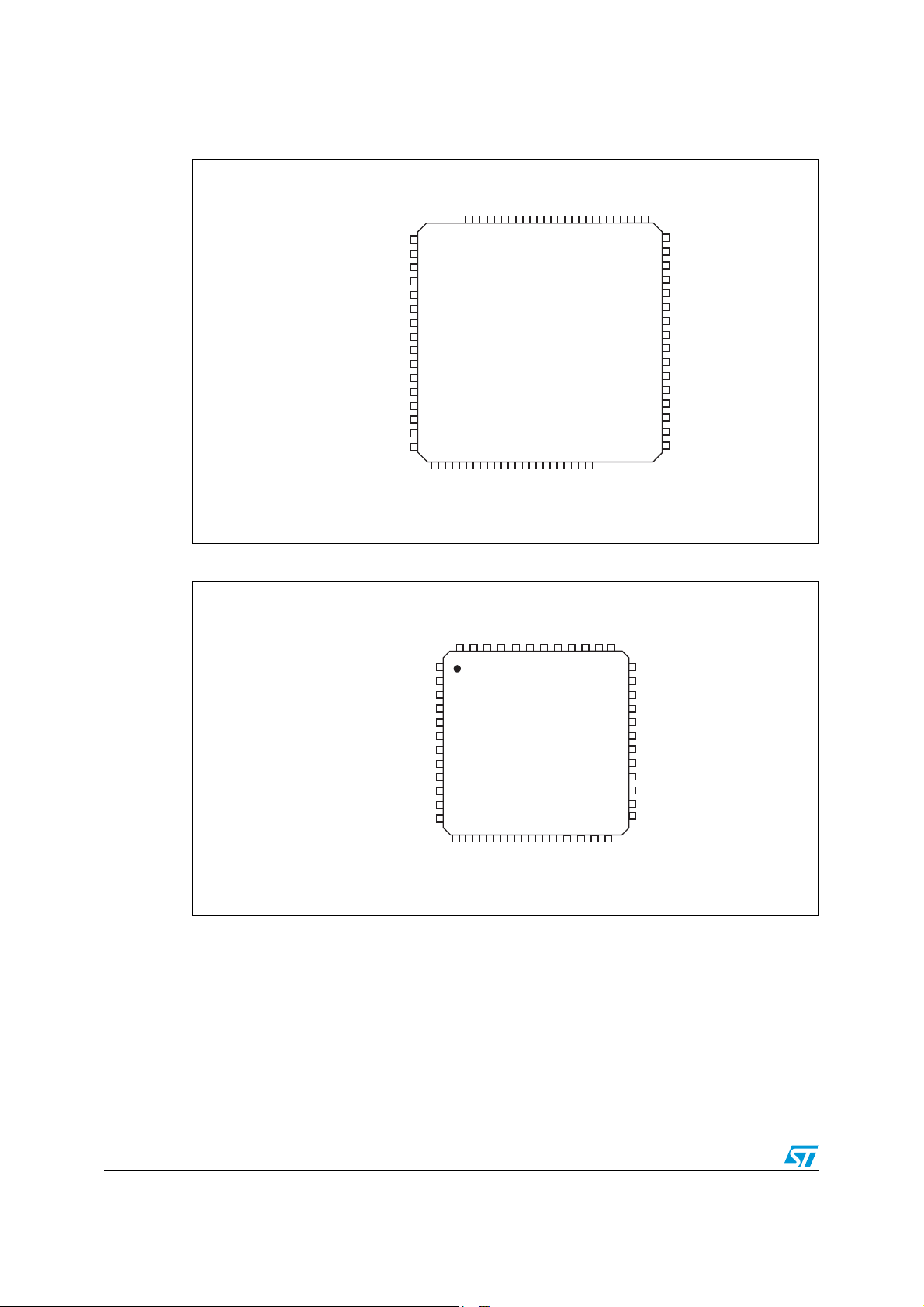
Figure 5. STM32L15xxx LQFP100 pinout . . . . . . . . . . . . . . . . . . . . . . . . . . . . . . . . . . . . . . . . . . . . . 27
Figure 6. STM32L15xxx LQFP64 pinout . . . . . . . . . . . . . . . . . . . . . . . . . . . . . . . . . . . . . . . . . . . . . . 28
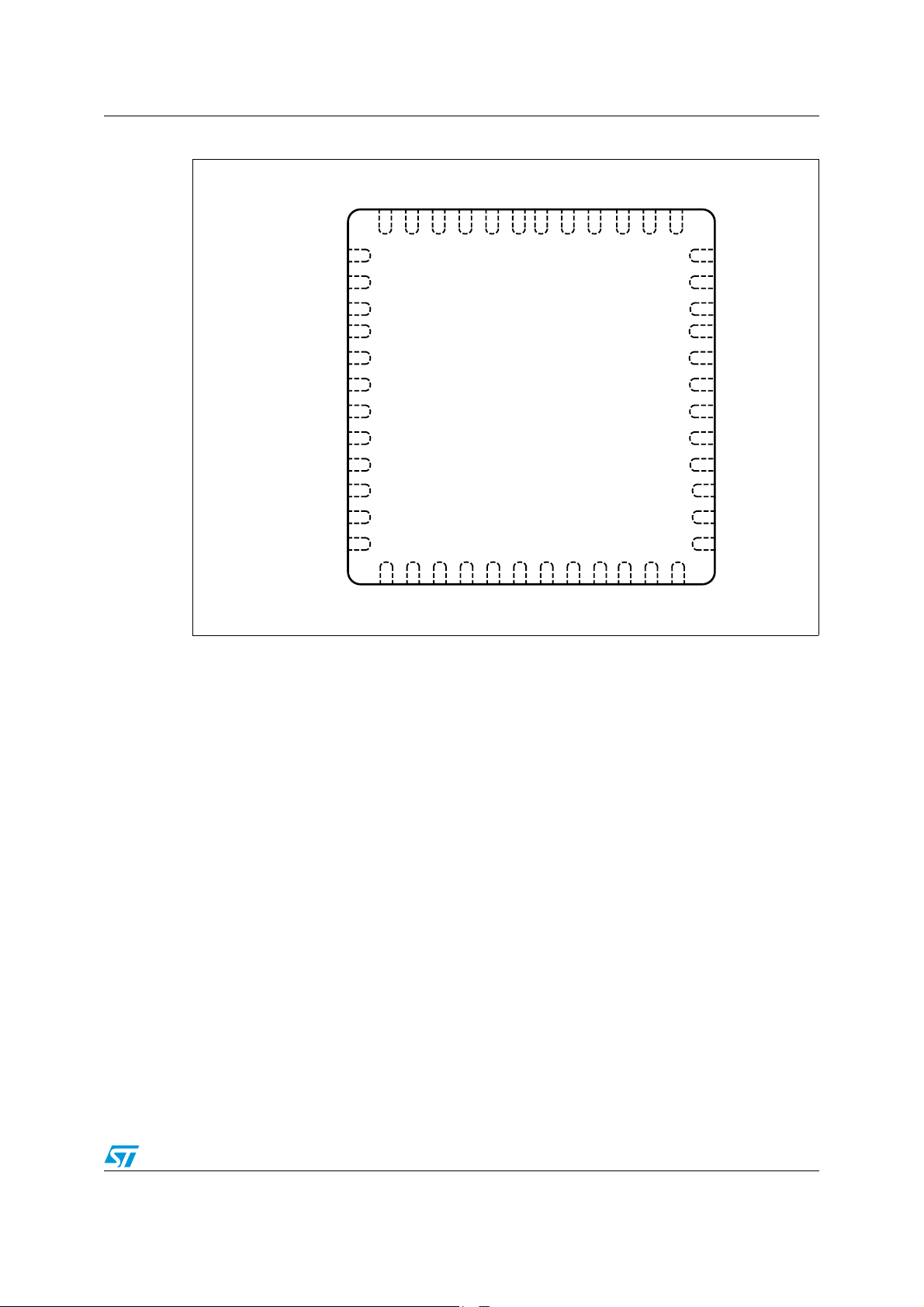
Figure 7. STM32L15xxx LQFP48 pinout . . . . . . . . . . . . . . . . . . . . . . . . . . . . . . . . . . . . . . . . . . . . . . 28
Figure 8. STM32L15xxx UFQFPN48 pinout . . . . . . . . . . . . . . . . . . . . . . . . . . . . . . . . . . . . . . . . . . . 29
Figure 9. Memory map . . . . . . . . . . . . . . . . . . . . . . . . . . . . . . . . . . . . . . . . . . . . . . . . . . . . . . . . . . . . 40
Figure 10. Pin loading conditions . . . . . . . . . . . . . . . . . . . . . . . . . . . . . . . . . . . . . . . . . . . . . . . . . . . . . 41
Figure 11. Pin input voltage . . . . . . . . . . . . . . . . . . . . . . . . . . . . . . . . . . . . . . . . . . . . . . . . . . . . . . . . . 41
Figure 12. Power supply scheme. . . . . . . . . . . . . . . . . . . . . . . . . . . . . . . . . . . . . . . . . . . . . . . . . . . . . 42
Figure 13. Current consumption measurement scheme . . . . . . . . . . . . . . . . . . . . . . . . . . . . . . . . . . . 42
Figure 14. Low-speed external clock source AC timing diagram . . . . . . . . . . . . . . . . . . . . . . . . . . . . . 60
Figure 15. High-speed external clock source AC timing diagram . . . . . . . . . . . . . . . . . . . . . . . . . . . . 61
Figure 16. HSE oscillator circuit diagram. . . . . . . . . . . . . . . . . . . . . . . . . . . . . . . . . . . . . . . . . . . . . . . 63
Figure 17. Typical application with a 32.768 kHz crystal . . . . . . . . . . . . . . . . . . . . . . . . . . . . . . . . . . . 64
Figure 18. I/O AC characteristics definition . . . . . . . . . . . . . . . . . . . . . . . . . . . . . . . . . . . . . . . . . . . . . 76
Figure 19. Recommended NRST pin protection . . . . . . . . . . . . . . . . . . . . . . . . . . . . . . . . . . . . . . . . . 77
Figure 20. I
Figure 21. SPI timing diagram - slave mode and CPHA = 0 . . . . . . . . . . . . . . . . . . . . . . . . . . . . . . . . 81
Figure 22. SPI timing diagram - slave mode and CPHA = 1
Figure 23. SPI timing diagram - master mode
Figure 24. USB timings: definition of data signal rise and fall time . . . . . . . . . . . . . . . . . . . . . . . . . . . 83
Figure 25. ADC accuracy characteristics . . . . . . . . . . . . . . . . . . . . . . . . . . . . . . . . . . . . . . . . . . . . . . . 87
Figure 26. Typical connection diagram using the ADC . . . . . . . . . . . . . . . . . . . . . . . . . . . . . . . . . . . . 87
Figure 27. Maximum dynamic current consumption on V
Figure 28. Power supply and reference decoupling (V
Figure 29. Power supply and reference decoupling (V
Figure 30. 12-bit buffered /non-buffered DAC . . . . . . . . . . . . . . . . . . . . . . . . . . . . . . . . . . . . . . . . . . . 92
Figure 31. UFQFPN48 7 x 7 mm, 0.5 mm pitch, package outline . . . . . . . . . . . . . . . . . . . . . . . . . . . . 97
Figure 32. Recommended footprint (dimensions in mm)
Figure 33. TFBGA64 - 8 x 8 active ball array, 5 x 5 mm, 0.5 mm pitch, package outline . . . . . . . . . . 98
Figure 34. Recommended PCB design rules for pads (0.5 mm pitch BGA) . . . . . . . . . . . . . . . . . . . . 99
Figure 35. UFBGA100 - ultra fine pitch ball grid array, 7 x 7 mm, 0.50 mm pitch,
Figure 36. LQFP100, 14 x 14 mm, 100-pin low-profile quad flat package outline . . . . . . . . . . . . . . . 101
Figure 37. Recommended footprint
Figure 38. LQFP64, 10 x 10 mm, 64-pin low-profile quad flat package outline . . . . . . . . . . . . . . . . . 102
Figure 39. Recommended footprint
Figure 40. LQFP48, 7 x 7 mm, 48-pin low-profile quad flat package outline . . . . . . . . . . . . . . . . . . . 103
Figure 41. Recommended footprint
2
C bus AC waveforms and measurement circuit . . . . . . . . . . . . . . . . . . . . . . . . . . . . . . . . 79
(1)
(1)
. . . . . . . . . . . . . . . . . . . . . . . . . . . . . . . . . . . . . . . . . 82
. . . . . . . . . . . . . . . . . . . . . . . . . . . . . . 81
supply pin during ADC
REF+
conversion . . . . . . . . . . . . . . . . . . . . . . . . . . . . . . . . . . . . . . . . . . . . . . . . . . . . . . . . . . . . . 88
not connected to V
REF+
connected to V
REF+
(1)
. . . . . . . . . . . . . . . . . . . . . . . . . . . . . . . . . 97
DDA
). . . . . . . . . . . . . . 89
DDA
). . . . . . . . . . . . . . . . . 89
package outline. . . . . . . . . . . . . . . . . . . . . . . . . . . . . . . . . . . . . . . . . . . . . . . . . . . . . . . . . 100
(1)
. . . . . . . . . . . . . . . . . . . . . . . . . . . . . . . . . . . . . . . . . . . . . . . . 101
(1)
. . . . . . . . . . . . . . . . . . . . . . . . . . . . . . . . . . . . . . . . . . . . . . . . 102
(1)
. . . . . . . . . . . . . . . . . . . . . . . . . . . . . . . . . . . . . . . . . . . . . . . . 103
Doc ID 17659 Rev 6 7/109
Page 8

Introduction STM32L151xx, STM32L152xx
1 Introduction
This datasheet provides the ordering information and mechanical device characteristics of
the STM32L151xx and STM32L152xx ultralow power ARM Cortex™-based microcontrollers
product line.
The ultralow power STM32L15xxx family includes devices in 3 different package types: from
48 pins to 100 pins. Depending on the device chosen, different sets of peripherals are
included, the description below gives an overview of the complete range of peripherals
proposed in this family.
These features make the ultralow power STM32L15xxx microcontroller family suitable for a
wide range of applications:
● Medical and handheld equipment
● Application control and user interface
● PC peripherals, gaming, GPS and sport equipment
● Alarm systems, Wired and wireless sensors, Video intercom
● Utility metering
For information on the Cortex™-M3 core please refer to the Cortex™-M3 Technical
Reference Manual, available from the www.arm.com website at the following address:
http://infocenter.arm.com/help/index.jsp?topic=/com.arm.doc.ddi0337g.
Figure 1 shows the general block diagram of the device family.
8/109 Doc ID 17659 Rev 6
Page 9

STM32L151xx, STM32L152xx Description
2 Description
The ultralow power STM32L15xxx incorporates the connectivity power of the universal
serial bus (USB) with the high-performance ARM Cortex
a 32
MHz frequency, a memory protection unit (MPU), high-speed embedded memories
(Flash memory up to 128
enhanced I/Os and peripherals connected to two APB buses. All devices offer a 12-bit ADC,
2 DACs and 2 ultralow power comparators, six general-purpose 16-bit timers and two basic
timers, which can be used as time bases. Moreover, the STM32L15xxx devices contain
standard and advanced communication interfaces: up to two I
and a USB. They also include a real-time clock and a set of backup registers that remain
powered in Standby mode. Finally, the integrated LCD controller has a built-in LCD voltage
generator that allows you to drive up to 8 multiplexed LCDs with contrast independent of the
supply voltage.
The ultralow power STM32L15xxx operates from a 1.8 to 3.6 V power supply (down to
1.65
V at power down) with BOR and from a 1.65 to 3.6 V power supply without BOR option.
It is available in the -40 to +85
modes allows the design of low-power applications.
Kbytes and RAM up to 16 Kbytes), and an extensive range of
°C temperature range. A comprehensive set of power-saving
™
-M3 32-bit RISC core operating at
2
Cs and SPIs, three USARTs
Doc ID 17659 Rev 6 9/109
Page 10
Description STM32L151xx, STM32L152xx
2.1 Device overview
Table 2. Ultralow power STM32L15xxx device features and peripheral counts
Flash - Kbytes 32 64 128 32 64 128 64 128
RAM - Kbytes 10 10 16 10 10 16 10 16
Timers
Communication
interfaces
GPIOs 37 51 83
12-bit synchronized ADC
Number of channels
12-bit DAC
Number of channels
Peripheral
Generalpurpose
Basic 222
SPI 222
2
I
USART 333
USB 111
STM32L15xCx STM32L15xRx STM32L15xVx
666
C 222
1
16 channels
2
2
1
20 channels
2
2
1
24 channels
2
2
LCD (STM32L152xx Only)
COM x SEG
Comparator 222
CPU frequency 32 MHz
Operating voltage
Operating temperatures
Packages LQFP48, UFQFPN48 LQFP64, BGA64 LQFP100, BGA100
Ambient temperatures: –40 to +85 °C
Junction temperature: –40 to + 105 °C
4x16
1.8 V to 3.6 V (down to 1.65 V at power-down)
1.65 V to 3.6 V without BOR option
4x32
8x28
with BOR option
4x44
8x40
.
10/109 Doc ID 17659 Rev 6
Page 11

STM32L151xx, STM32L152xx Description
2.2 Ultralow power device continuum
The ultralow power STM32L151xx and STM32L152xx are fully pin-to-pin, software and
feature compatible. Besides the full compatibility within the family, the devices are part of
STMicroelectronics microcontrollers ultralow power strategy which also includes
STM8L101xx and STM8L15xx devices. The STM8L and STM32L families allow a
continuum of performance, peripherals, system architecture and features.
They are all based on STMicroelectronics 0.13 µm ultralow leakage process.
Note: The ultralow power STM32L and general-purpose STM32Fxxxx families are pin-to-pin
compatible. The STM8L15xxx devices are pin-to-pin compatible with the STM8L101xx
devices. Please refer to the STM32F and STM8L documentation for more information on
these devices.
2.2.1 Performance
All families incorporate highly energy-efficient cores with both Harvard architecture and
pipelined execution: advanced STM8 core for STM8L families and ARM Cortex™-M3 core
for STM32L family. In addition specific care for the design architecture has been taken to
optimize the mA/DMIPS and mA/MHz ratios.
This allows the ultralow power performance to range from 5 up to 33.3 DMIPs.
2.2.2 Shared peripherals
STM8L15xxx and STM32L15xxx share identical peripherals which ensure a very easy
migration from one family to another:
● Analog peripherals: ADC, DAC, and comparators
● Digital peripherals: RTC and some communication interfaces
2.2.3 Common system strategy
To offer flexibility and optimize performance, the STM8L15xx and STM32L15xx families use
a common architecture:
● Same power supply range from 1.65 V to 3.6 V, (1.65 V at power down only for
STM8L15xx devices)
● Architecture optimized to reach ultralow consumption both in low power modes and
Run mode
● Fast startup strategy from low power modes
● Flexible system clock
● Ultrasafe reset: same reset strategy including power-on reset, power-down reset,
brownout reset and programmable voltage detector.
2.2.4 Features
ST ultralow power continuum also lies in feature compatibility:
● More than 10 packages with pin count from 20 to 100 pins and size down to 3 x 3 mm
● Memory density ranging from 4 to 128 Kbytes
Doc ID 17659 Rev 6 11/109
Page 12
Functional overview STM32L151xx, STM32L152xx
%84)4
77$'
BIT!$#
*4!'37
!&
*4$)
*4#+37#+
*4-337$
.*4234
*4$/
.234
6$$6TO6
!&
!("
53"$0
53"$-
-/3)-)3/3#+.33
7+50
&
MAX
-(Z
6
33
3#,3$!3-"U S0-"U S
)#
6
$$2%&?!$#
'0$-!
4)-
4)-
84!,/3#
-(Z
84!,K(Z
/3#?).
/3#?/54
/3#?/54
/3#?).
0,,
!0"&
MAX
-(Z
!("0#, +
(#,+
CLOCK
MANAGEMENT
!0"0#, +
AS!&
AS!&
6/,4 2%'
6
#/2%
0/7%2
AS!&
4)-
"US -ATRI X
)NTER FACE
24#
2#(3
)BUS
$BUS
PBUS
OBL
&LASH
53"2!-"
53!24
53!24
30)
CHANNELS
3#,3$!
)#
AS!&
2848#43243
53!24
4EMPS ENSOR
6
332%&?!$#
!("&
MAX
-(Z
#HANN ELS
#HANN ELS
#HANN ELS
&#,+
)7$'
6$$
3UPPLY
MONITORING
6$$!
6$$!
633!
6$$!
3MART# ARDAS !&
2848#43243
3MART #ARD AS!&
2848#43243
3MART#A RDAS !&
!0" &
MAX
-(Z
.6)#
30)
-/3)-)3/
3#+.33AS!&
)&
6$$!
06$
0OWERRESET
)NT
!("
!0"
!0"
!7 5
6$$!
24#?!&
3YST EM
0!; =
0"; =
0#;=
0$;=
0%;=
,#$XX
3%'X
#/-X
)&)&)&
6$$!
$!#AS!&
$!#AS! &
-05
#OMP
#/-0?). ).
#OMP
4)-
4)--
4)-
4)-
4)-
#HANNE LS
#HANNEL
#HANNEL
'ENERALPURPOSE
TIMERS
+"&LASH
+"DATA%%02/-
,#$STEPUP
CONVERTER
6
,#$
6TO6
6
,#$
"!3)#4)-%23
3YNC (Z
62%&/54054
AIE
#ORTEX-#05
4RACECONTROLLER
%4-
2!-
+"
BIT$!#
BIT$!#
'0)/!
'0)/"
'0)/#
'0)/$
'0)/%
42!#%#+42!#%$
42!#%$42!#%$
42!#%$
2#-3
2#,3
3TANDBYINTERFACE
"ACKUPINTERFACE
53"&3DEVICE
"/262%&).4
0OWERUP
0OWERDOWN
"ACKUP
REGISTER
0(;=
'0)/(
3 Functional overview
Figure 1 shows the block diagrams.
Figure 1. Ultralow power STM32L15xxx block diagram
12/109 Doc ID 17659 Rev 6
1. AF = alternate function on I/O port pin.
Page 13

STM32L151xx, STM32L152xx Functional overview
3.1 Low power modes
The ultralow power STM32L15xxx supports dynamic voltage scaling to optimize its power
consumption in run mode. The voltage from the internal low-drop regulator that supplies the
logic can be adjusted according to the system’s maximum operating frequency and the
external voltage supply:
● In range 1 (V
Table 13 for consumption).
● In range 2 (full V
consumption)
● In range 3 (full V
multispeed internal RC oscillator clock source). Refer to Table 13 for consumption.
Seven low power modes are provided to achieve the best compromise between low power
consumption, short startup time and available wakeup sources:
● Sleep mode
In Sleep mode, only the CPU is stopped. All peripherals continue to operate and can
wake up the CPU when an interrupt/event occurs.
Sleep mode power consumption: refer to Ta bl e 1 5.
● Low power run mode
This mode is achieved with the multispeed internal (MSI) RC oscillator set to the
minimum clock (65 kHz), execution from SRAM or Flash memory, and internal regulator
in low power mode to minimize the regulator's operating current. In the Low power run
mode, the clock frequency and the number of enabled peripherals are both limited.
Low power run mode consumption: refer to Table 16.
● Low power sleep mode
This mode is achieved by entering the Sleep mode with the internal voltage regulator in
Low power mode to minimize the regulator’s operating current. In the Low power sleep
mode, both the clock frequency and the number of enabled peripherals are limited; a
typical example would be to have a timer running at 32 kHz.
When wakeup is triggered by an event or an interrupt, the system reverts to the run
mode with the regulator on.
Low power sleep mode consumption: refer to Table 17.
● Stop mode (with or without RTC)
The Stop mode achieves the lowest power consumption while retaining the RAM and
register contents. All clocks in the V
RC and HSE crystal oscillators are disabled. The voltage regulator is in the low power
mode.
The device can be woken up from the Stop mode by any of the EXTI line, in 8 µs. The
EXTI line source can be one of the 16 external lines, the PVD output, the RTC alarm(s),
the USB wakeup, the RTC tamper event, the RTC timestamp event, the RTC Wakeup,
the Comparator 1 event or Comparator 2 event.
Stop mode consumption: refer to Tab le 18 .
range limited to 2.0-3.6 V), the CPU runs at up to 32 MHz (refer to
DD
range), the CPU runs at up to 16 MHz (refer to Table 13 for
DD
range), the CPU runs at up to 4 MHz (generated only with the
DD
domain are stopped, the PLL, MSI RC, HSI
CORE
Doc ID 17659 Rev 6 13/109
Page 14

Functional overview STM32L151xx, STM32L152xx
● Standby mode (with or without RTC)
The Standby mode is used to achieve the lowest power consumption. The internal
voltage regulator is switched off so that the entire V
domain is powered off. The
CORE
PLL, MSI RC, HSI RC and HSE crystal oscillators are also switched off. After entering
Standby mode, the RAM and register contents are lost except for registers in the
Standby circuitry (wakeup logic, IWDG, RTC, LSI, LSE Crystal 32K osc, RCC CSR).
The device exits the Standby mode in 60 µs when an external reset (NRST pin), an
IWDG reset, a rising edge on one of the three WKUP pins, RTC alarm (Alarm A or
Alarm B), RTC tamper event, RTC timestamp event or RTC Wakeup event.
Standby mode consumption: refer to Table 19.
Note: The RTC, the IWDG, and the corresponding clock sources are not stopped by entering the
Stop or Standby mode.
3.2 ARM® Cortex™-M3 core with MPU
The ARM Cortex™-M3 processor is the latest generation of ARM processors for embedded
systems. It has been developed to provide a low-cost platform that meets the needs of MCU
implementation, with a reduced pin count and low-power consumption, while delivering
outstanding computational performance and an advanced system response to interrupts.
The ARM Cortex™-M3 32-bit RISC processor features exceptional code-efficiency,
delivering the high-performance expected from an ARM core in the memory size usually
associated with 8- and 16-bit devices.
The memory protection unit (MPU) improves system reliability by defining the memory
attributes (such as read/write access permissions) for different memory regions. It provides
up to eight different regions and an optional predefined background region.
Owing to its embedded ARM core, the STM32L15xxx is compatible with all ARM tools and
software.
Nested vectored interrupt controller (NVIC)
The ultralow power STM32L15xxx embeds a nested vectored interrupt controller able to
handle up to 45 maskable interrupt channels (not including the 16 interrupt lines of
Cortex™-M3) and 16 priority levels.
● Closely coupled NVIC gives low-latency interrupt processing
● Interrupt entry vector table address passed directly to the core
● Closely coupled NVIC core interface
● Allows early processing of interrupts
● Processing of late arriving, higher-priority interrupts
● Support for tail-chaining
● Processor state automatically saved
● Interrupt entry restored on interrupt exit with no instruction overhead
This hardware block provides flexible interrupt management features with minimal interrupt
latency.
14/109 Doc ID 17659 Rev 6
Page 15

STM32L151xx, STM32L152xx Functional overview
3.3 Reset and supply management
3.3.1 Power supply schemes
● V
● V
= 1.65 to 3.6 V: external power supply for I/Os and the internal regulator.
DD
Provided externally through V
, V
SSA
= 1.65 to 3.6 V: external analog power supplies for ADC, reset blocks, RCs
DDA
and PLL (minimum voltage to be applied to V
V
DDA
and V
must be connected to V
SSA
DD
pins.
is 1.8 V when the ADC is used).
DDA
and VSS, respectively.
DD
3.3.2 Power supply supervisor
The device has an integrated ZEROPOWER power-on reset (POR)/power-down reset
(PDR) that can be coupled with a brownout reset (BOR) circuitry.
For devices operating between 1.8 and 3.6 V, the BOR is always active at power-on and
ensures proper operation starting from 1.8
option byte loading process starts, either to confirm or modify default thresholds, or to
disable BOR permanently (in which case, the V
BOR thresholds are available through option bytes, starting from 1.8
power consumption in Stop mode, it is possible to automatically switch off the internal
reference voltage (V
below a specified threshold, V
) in Stop mode. The device remains in reset mode when V
REFINT
POR/PDR
circuit.
Note: For devices operating between 1.65 V and 3.6 V, the BOR is permanently disabled.
Consequently, the start-up time at power-on can be decreased down to 1ms typically.
The device features an embedded programmable voltage detector (PVD) that monitors the
V
DD/VDDA
levels between 1.85
interrupt can be generated when V
V
DD/VDDA
power supply and compares it to the V
V and 3.05 V, chosen by software, with a step around 200 mV. An
is higher than the V
DD/VDDA
threshold. The interrupt service routine can then generate
PVD
a warning message and/or put the MCU into a safe state. The PVD is enabled by software.
V. After the 1.8 V BOR threshold is reached, the
min value at power down is 1.65 V). Five
DD
V to 3 V. To reduce the
or V
, without the need for any external reset
BOR
threshold. This PVD offers 7 different
PVD
drops below the V
threshold and/or when
PVD
DD
is
3.3.3 Voltage regulator
The regulator has three operation modes: main (MR), low power (LPR) and power down.
● MR is used in Run mode (nominal regulation)
● LPR is used in the Low-power run, Low-power sleep and Stop modes
● Power down is used in Standby mode. The regulator output is high impedance, the
kernel circuitry is powered down, inducing zero consumption but the contents of the
registers and RAM are lost are lost except for the standby circuitry (wakeup logic,
IWDG, RTC, LSI, LSE crystal 32K osc, RCC_CSR).
Doc ID 17659 Rev 6 15/109
Page 16

Functional overview STM32L151xx, STM32L152xx
3.3.4 Boot modes
At startup, boot pins are used to select one of three boot options:
● Boot from Flash memory
● Boot from System Memory
● Boot from embedded RAM
The boot loader is located in System Memory. It is used to reprogram the Flash memory by
using USART1 or USART2. For further details please refer to AN2606.
3.4 Clock management
The clock controller distributes the clocks coming from different oscillators to the core and
the peripherals. It also manages clock gating for low power modes and ensures clock
robustness. It features:
● Clock prescaler: to get the best tradeoff between speed and current consumption, the
clock frequency to the CPU and peripherals can be adjusted by a programmable
prescaler
● Safe clock switching: clock sources can be changed safely on the fly in run mode
through a configuration register.
● Clock management: to reduce power consumption, the clock controller can stop the
clock to the core, individual peripherals or memory.
● Master clock source: three different clock sources can be used to drive the master
clock:
– 1-24 MHz high-speed external crystal (HSE), that can supply a PLL
– 16 MHz high-speed internal RC oscillator (HSI), trimmable by software, that can
supply a PLL
– Multispeed internal RC oscillator (MSI), trimmable by software, able to generate 7
frequencies (65.5 kHz, 131 kHz, 262 kHz, 524 kHz, 1.05 MHz, 2.1 MHz, 4.2 MHz)
with a consumption proportional to speed, down to 750 nA typical. When a
32.768 kHz clock source is available in the system (LSE), the MSI frequency can
be trimmed by software down to a ±0.5% accuracy.
● Auxiliary clock source: two ultralow power clock sources that can be used to drive the
LCD controller and the real-time clock:
– 32.768 kHz low-speed external crystal (LSE)
– 37 kHz low-speed internal RC (LSI), also used to drive the independent watchdog.
The LSI clock can be measured using the high-speed internal RC oscillator for
greater precision.
● RTC and LCD clock sources: the LSI, LSE or HSE sources can be chosen to clock
the RTC and the LCD, whatever the system clock.
● USB clock source: the embedded PLL has a dedicated 48 MHz clock output to supply
the USB interface.
● Startup clock: after reset, the microcontroller restarts by default with an internal
2.1 MHz clock (MSI). The prescaler ratio and clock source can be changed by the
application program as soon as the code execution starts.
16/109 Doc ID 17659 Rev 6
Page 17
STM32L151xx, STM32L152xx Functional overview
● Clock security system (CSS): this feature can be enabled by software. If a HSE clock
failure occurs, the master clock is automatically switched to HSI and a software
interrupt is generated if enabled.
● Clock-out capability (MCO: microcontroller clock output): it outputs one of the
internal clocks for external use by the application.
Several prescalers allow the configuration of the AHB frequency, the high-speed APB
(APB2) and the low-speed APB (APB1) domains. The maximum frequency of the AHB and
the APB domains is 32 MHz. See
Figure 2 for details on the clock tree.
Figure 2. Clock tree
/3#?/54
/3#?).
/3#?).
/3#?/54
-#/
-3)2#
-(Z
(3)2#
-(Z
(3%/3#
,3%/3#
K(Z
,3)2#
K(Z
(3)
0,,32#
,3%
-#/3%,
-3)
XXXX
XXX
24#3%,;=
,3)
393#,+
(3)
-3)
(3%
0,,#,+
,3)
,3%
0ERIPHERALCLOCK
ENABLE
0,,6#/
0,,-5,
XX
24##,+
TO)NDEPENDENT7ATCHDOG)7 $'
0RESCALER
0,,$)6
!("
TO
4IMER%42
TO24#
TO,#$
)7$'#,+
!$##,+
-(Z
53"#,+
TO53"INTERFACE
-(ZMAX
#LOCK
%NABLE
!0"
0RESCALER
)F!0"PRESCALERX
!0"
0RESCALER
)F!0"PRESCALERX
TO!$#
ELSEX
,EGEND
(3%(IGHSPEEDEXTERNALCLOCKSIGNAL
(3) (IGHSPEEDINTERNALCLOCKSIGNAL
,3),OWSPEEDINTERNALCLOCKSIGNAL
,3%,OWSPEEDEXTERNALCLOCKSIGNAL
-3)-ULTISPEEDINTERNALCLOCKSIGNAL
37
(3)
0,,#,+
(3%
#33
(#,+
TO!("BUSCORE
MEMORYAND$-!
TO#ORTEX3YSTEMTIMER
&#,+#ORTEX
FREERUNNINGCLOCK
-(ZMAX
0ERIPHERAL#LOCK
%NABLE
0ERIPHERAL#LOCK
%NABLE
-(ZMAX
0ERIPHERAL#LOCK
%NABLE
ELSEX
0ERIPHERAL#LOCK
%NABLE
393#,+
0#,+
TO!0"
PERIPHERALS
TO4)-AND
4)-X#,+
0#,+
PERIPHERALSTO!0"
TO4)-AND
4)-X#,+
-(Z
MAX
AIC
2. For the USB function to be available, both HSE and PLL must be enabled, with the CPU running at either
24 MHz or 32 MHz.
Doc ID 17659 Rev 6 17/109
Page 18

Functional overview STM32L151xx, STM32L152xx
3.5 Low power real-time clock and backup registers
The real-time clock (RTC) is an independent BCD timer/counter. Dedicated registers contain
the second, minute, hour (12/24 hour), week day, date, month, year, in BCD (binary-coded
decimal) format. Correction for 28, 29 (leap year), 30, and 31 day of the month are made
automatically. The RTC provides a programmable alarm and programmable periodic
interrupts with wakeup from Stop and Standby modes.
● The programmable wakeup time ranges from 120 µs to 36 hours
● Stop mode consumption with LSI and Auto-wakeup: 1.2 µA (at 1.8 V) and 1.4 µA (at
3.0 V)
● Stop mode consumption with LSE, calendar and Auto-wakeup: 1.3 µA (at 1.8V), 1.6 µA
(at 3.0 V)
The RTC can be calibrated with an external 512 Hz output, and a digital compensation
circuit helps reduce drift due to crystal deviation.
There are twenty 32-bit backup registers provided to store 80 bytes of user application data.
They are cleared in case of tamper detection.
3.6 GPIOs (general-purpose inputs/outputs)
Each of the GPIO pins can be configured by software as output (push-pull or open-drain), as
input (with or without pull-up or pull-down) or as peripheral alternate function. Most of the
GPIO pins are shared with digital or analog alternate functions, and can be individually
remapped using dedicated AFIO registers. All GPIOs are high-current-capable. The
alternate function configuration of I/Os can be locked if needed following a specific
sequence in order to avoid spurious writing to the I/O registers. The I/O controller is
connected to the AHB with a toggling speed of up to 16 MHz.
External interrupt/event controller (EXTI)
The external interrupt/event controller consists of 23 edge detector lines used to generate
interrupt/event requests. Each line can be individually configured to select the trigger event
(rising edge, falling edge, both) and can be masked independently. A pending register
maintains the status of the interrupt requests. The EXTI can detect an external line with a
pulse width shorter than the Internal APB2 clock period. Up to 83 GPIOs can be connected
to the 16 external interrupt lines.
18/109 Doc ID 17659 Rev 6
Page 19

STM32L151xx, STM32L152xx Functional overview
3.7 Memories
The STM32L15xxx devices have the following features:
● Up to 16 Kbyte of embedded RAM accessed (read/write) at CPU clock speed with 0
wait states. With the enhanced bus matrix, operating the RAM does not lead to any
performance penalty during accesses to the system bus (AHB and APB buses).
● The non-volatile memory is divided into three arrays:
– 32, 64 or 128 Kbyte of embedded Flash program memory
– 4 Kbyte of data EEPROM
– Options bytes
The options bytes are used to write-protect the memory (with 4 KB granularity) and/or
readout-protect the whole memory with the following options:
– Level 0: no readout protection
– Level 1: memory readout protection, the Flash memory cannot be read from or
written to if either debug features are connected or boot in RAM is selected
– Level 2: chip readout protection, debug features (Cortex-M3 JTAG and serial wire)
and boot in RAM selection disabled (JTAG fuse)
The whole non-volatile memory embeds the error correction code (ECC) feature.
3.8 DMA (direct memory access)
The flexible 7-channel, general-purpose DMA is able to manage memory-to-memory,
peripheral-to-memory and memory-to-peripheral transfers. The DMA controller supports
circular buffer management, avoiding the generation of interrupts when the controller
reaches the end of the buffer.
Each channel is connected to dedicated hardware DMA requests, with software trigger
support for each channel. Configuration is done by software and transfer sizes between
source and destination are independent.
The DMA can be used with the main peripherals: SPI, I2C, USART, general-purpose timers
and ADC.
3.9 LCD (liquid crystal display)
The LCD drives up to 8 common terminals and 44 segment terminals to drive up to 320
pixels.
● Internal step-up converter to guarantee functionality and contrast control irrespective of
V
. This converter can be deactivated, in which case the V
DD
the voltage to the LCD
● Supports static, 1/2, 1/3, 1/4 and 1/8 duty
● Supports static, 1/2, 1/3 and 1/4 bias
● Phase inversion to reduce power consumption and EMI
● Up to 8 pixels can be programmed to blink
● Unneeded segments and common pins can be used as general I/O pins
● LCD RAM can be updated at any time owing to a double-buffer
● The LCD controller can operate in Stop mode
pin is used to provide
LCD
Doc ID 17659 Rev 6 19/109
Page 20

Functional overview STM32L151xx, STM32L152xx
3.10 ADC (analog-to-digital converter)
A 12-bit analog-to-digital converters is embedded into STM32L15xxx devices with up to 24
external channels, performing conversions in single-shot or scan mode. In scan mode,
automatic conversion is performed on a selected group of analog inputs.
The ADC can be served by the DMA controller.
An analog watchdog feature allows very precise monitoring of the converted voltage of one,
some or all selected channels. An interrupt is generated when the converted voltage is
outside the programmed thresholds.
The events generated by the general-purpose timers (TIMx) can be internally connected to
the ADC start trigger and injection trigger, to allow the application to synchronize A/D
conversions and timers.
The ADC includes a specific low power mode. The converter is able to operate at maximum
speed even if the CPU is operating at a very low frequency and has an auto-shutdown
function. The ADC’s runtime and analog front-end current consumption are thus minimized
whatever the MCU operating mode.
Temperature sensor
The temperature sensor has to generate a voltage that varies linearly with temperature. The
conversion range is between 1.8 V < V
connected to the ADC_IN16 input channel.
< 3.6 V. The temperature sensor is internally
DDA
3.11 DAC (digital-to-analog converter)
The two 12-bit buffered DAC channels can be used to convert two digital signals into two
analog voltage signal outputs. The chosen design structure is composed of integrated
resistor strings and an amplifier in non-inverting configuration.
This dual digital Interface supports the following features:
● two DAC converters: one for each output channel
● left or right data alignment in 12-bit mode
● synchronized update capability
● noise-wave generation
● triangular-wave generation
● dual DAC channels’ independent or simultaneous conversions
● DMA capability for each channel (including the underrun interrupt)
● external triggers for conversion
● input reference voltage V
Eight DAC trigger inputs are used in the STM32L15xxx. The DAC channels are triggered
through the timer update outputs that are also connected to different DMA channels.
REF+
20/109 Doc ID 17659 Rev 6
Page 21
STM32L151xx, STM32L152xx Functional overview
3.12 Ultralow power comparators and reference voltage
The STM32L15xxx embeds two comparators sharing the same current bias and reference
voltage. The reference voltage can be internal or external (coming from an I/O).
● one comparator with fixed threshold
● one comparator with rail-to-rail inputs, fast or slow mode. The threshold can be one of
the following:
– DAC output
– External I/O
– Internal reference voltage (V
REFINT
) or V
submultiple (1/4, 1/2, 3/4)
REFINT
Both comparators can wake up from Stop mode, and be combined into a window
comparator.
The internal reference voltage is available externally via a low power / low current output
buffer (driving current capability of 1
µA typical).
3.13 Routing interface
This interface controls the internal routing of I/Os to TIM2, TIM3, TIM4 and to the
comparator and reference voltage output.
3.14 Timers and watchdogs
The ultralow power STM32L15xxx devices include six general-purpose timers, two basic
timers and two watchdog timers.
Ta bl e 3 compares the features of the general-purpose and basic timers.
Table 3. Timer feature comparison
Timer
TIM2,
TIM3,
TIM4
TIM9 16-bit Up
TIM10,
TIM11
TIM6,
TIM7
Counter
resolution
16-bit
16-bit Up
16-bit Up
Counter
type
Up,
down,
up/down
Prescaler
Any integer
between 1
and 65536
Any integer
between 1
and 65536
Any integer
between 1
and 65536
Any integer
between 1
and 65536
factor
DMA request
generation
Ye s 4 N o
No 2 No
No 1 No
Ye s 0 N o
Capture/compare
channels
Complementary
outputs
Doc ID 17659 Rev 6 21/109
Page 22

Functional overview STM32L151xx, STM32L152xx
3.14.1 General-purpose timers (TIM2, TIM3, TIM4, TIM9, TIM10 and TIM11)
There are six synchronizable general-purpose timers embedded in the STM32L15xxx
devices (see
TIM2, TIM3, TIM4
These timers are based on a 16-bit auto-reload up/downcounter and a 16-bit prescaler.
They feature 4 independent channels each for input capture/output compare, PWM or onepulse mode output. This gives up to 12 input captures/output compares/PWMs on the
largest packages.
The TIM2, TIM3, TIM4 general-purpose timers can work together or with the TIM10, TIM11
and TIM9 general-purpose timers via the Timer Link feature for synchronization or event
chaining. Their counter can be frozen in debug mode. Any of the general-purpose timers
can be used to generate PWM outputs.
TIM2, TIM3, TIM4 all have independent DMA request generation.
These timers are capable of handling quadrature (incremental) encoder signals and the
digital outputs from 1 to 3 hall-effect sensors.
TIM10, TIM11 and TIM9
These timers are based on a 16-bit auto-reload upcounter and a 16-bit prescaler. TIM10 and
TIM11 feature one independent channel, whereas TIM9 has two independent channels for
input capture/output compare, PWM or one-pulse mode output. They can be synchronized
with the TIM2, TIM3, TIM4 full-featured general-purpose timers.
Ta bl e 3 for differences).
They can also be used as simple time bases and be clocked by the LSE clock source
(32.768 kHz) to provide time bases independent from the main CPU clock.
3.14.2 Basic timers (TIM6 and TIM7)
These timers are mainly used for DAC trigger generation. They can also be used as generic
16-bit time bases.
3.14.3 SysTick timer
This timer is dedicated to the OS, but could also be used as a standard downcounter. It is
based on a 24-bit downcounter with autoreload capability and a programmable clock
source. It features a maskable system interrupt generation when the counter reaches 0.
3.14.4 Independent watchdog (IWDG)
The independent watchdog is based on a 12-bit downcounter and 8-bit prescaler. It is
clocked from an independent 37 kHz internal RC and, as it operates independently of the
main clock, it can operate in Stop and Standby modes. It can be used either as a watchdog
to reset the device when a problem occurs, or as a free-running timer for application timeout
management. It is hardware- or software-configurable through the option bytes. The counter
can be frozen in debug mode.
22/109 Doc ID 17659 Rev 6
Page 23

STM32L151xx, STM32L152xx Functional overview
3.14.5 Window watchdog (WWDG)
The window watchdog is based on a 7-bit downcounter that can be set as free-running. It
can be used as a watchdog to reset the device when a problem occurs. It is clocked from the
main clock. It has an early warning interrupt capability and the counter can be frozen in
debug mode.
3.15 Communication interfaces
3.15.1 I²C bus
Up to two I²C bus interfaces can operate in multimaster and slave modes. They can support
standard and fast modes.
They support dual slave addressing (7-bit only) and both 7- and 10-bit addressing in master
mode. A hardware CRC generation/verification is embedded.
They can be served by DMA and they support SM Bus 2.0/PM Bus.
3.15.2 Universal synchronous/asynchronous receiver transmitter (USART)
All USART interfaces are able to communicate at speeds of up to 4 Mbit/s. They provide
hardware management of the CTS and RTS signals. They support IrDA SIR ENDEC, are
ISO 7816 compliant and have LIN Master/Slave capability.
All USART interfaces can be served by the DMA controller.
3.15.3 Serial peripheral interface (SPI)
Up to two SPIs are able to communicate at up to 16 Mbits/s in slave and master modes in
full-duplex and simplex communication modes. The 3-bit prescaler gives 8 master mode
frequencies and the frame is configurable to 8 bits or 16 bits. The hardware CRC
generation/verification supports basic SD Card/MMC modes.
Both SPIs can be served by the DMA controller.
3.15.4 Universal serial bus (USB)
The STM32L15xxx embeds a USB device peripheral compatible with the USB full speed
12
Mbit/s. The USB interface implements a full speed (12 Mbit/s) function interface. It has
software-configurable endpoint setting and supports suspend/resume. The dedicated
48
MHz clock is generated from the internal main PLL (the clock source must use a HSE
crystal oscillator).
Doc ID 17659 Rev 6 23/109
Page 24

Functional overview STM32L151xx, STM32L152xx
3.16 CRC (cyclic redundancy check) calculation unit
The CRC (cyclic redundancy check) calculation unit is used to get a CRC code from a 32-bit
data word and a fixed generator polynomial.
Among other applications, CRC-based techniques are used to verify data transmission or
storage integrity. In the scope of the EN/IEC 60335-1 standard, they offer a means of
verifying the Flash memory integrity. The CRC calculation unit helps compute a signature of
the software during runtime, to be compared with a reference signature generated at linktime and stored at a given memory location.
3.17 Development support
Serial wire JTAG debug port (SWJ-DP)
The ARM SWJ-DP interface is embedded, and is a combined JTAG and serial wire debug
port that enables either a serial wire debug or a JTAG probe to be connected to the target.
The JTAG TMS and TCK pins are shared with SWDIO and SWCLK, respectively, and a
specific sequence on the TMS pin is used to switch between JTAG-DP and SW-DP.
The JTAG port can be permanently disabled with a JTAG fuse.
Embedded Trace Macrocell™
The ARM® Embedded Trace Macrocell provides a greater visibility of the instruction and
data flow inside the CPU core by streaming compressed data at a very high rate from the
STM32L15xxx through a small number of ETM pins to an external hardware trace port
analyzer (TPA) device. The TPA is connected to a host computer using USB, Ethernet, or
any other high-speed channel. Real-time instruction and data flow activity can be recorded
and then formatted for display on the host computer running debugger software. TPA
hardware is commercially available from common development tool vendors. It operates
with third party debugger software tools.
24/109 Doc ID 17659 Rev 6
Page 25
STM32L151xx, STM32L152xx Pin descriptions
ai17096d
A
B
E
D
C
F
G
H
J
K
L
M
PE3
OSC_IN
PC15
OSC32_OUT
PC14
RTC_AF1
WKUP2
PE4
OSC_OUT
PC0
VSSA
VREF-
VREF+
VDDA
PE1
PE5
PE2
PE6
WUKP3
VLCD
VSS_5
VDD_5
NRST
PC1
PC3
PA 0
WKUP1
PA 1
PB8
PE0
PB9
VSS_3
VSS_4
VDD_4
PC2
PA 2
PA 3
PA 4
BOOT0
PB7
VDD_3
PA 5
PA 6
PA 7
PD7
PB6
PB5
PC4
PC5
PB0
PD5
PD6
PB2
PB1
PB4
PD4
PE8
PE7
PB3
PD3
PD2
PD9
PE10
PE9
PA15
PD1
PD0
PD8
PE12
PE11
PA14
PC12
PC11
PC8
PA 9
PD15
PD12
PB15
PB10
PE13
PA 13
PC10
PH2
PA 8
PC7
PD14
PD11
PB14
PB11
PE14
VSS_2
VDD_2
PA12
PA11
PA10
PC9
PC6
PD13
PD10
PB13
PB12
PE15
VSS_1
VDD_1
2 3 4 5 6 7 8 9 10 11 12
1
PC13
PH0
PH1
OSC32_IN
4 Pin descriptions
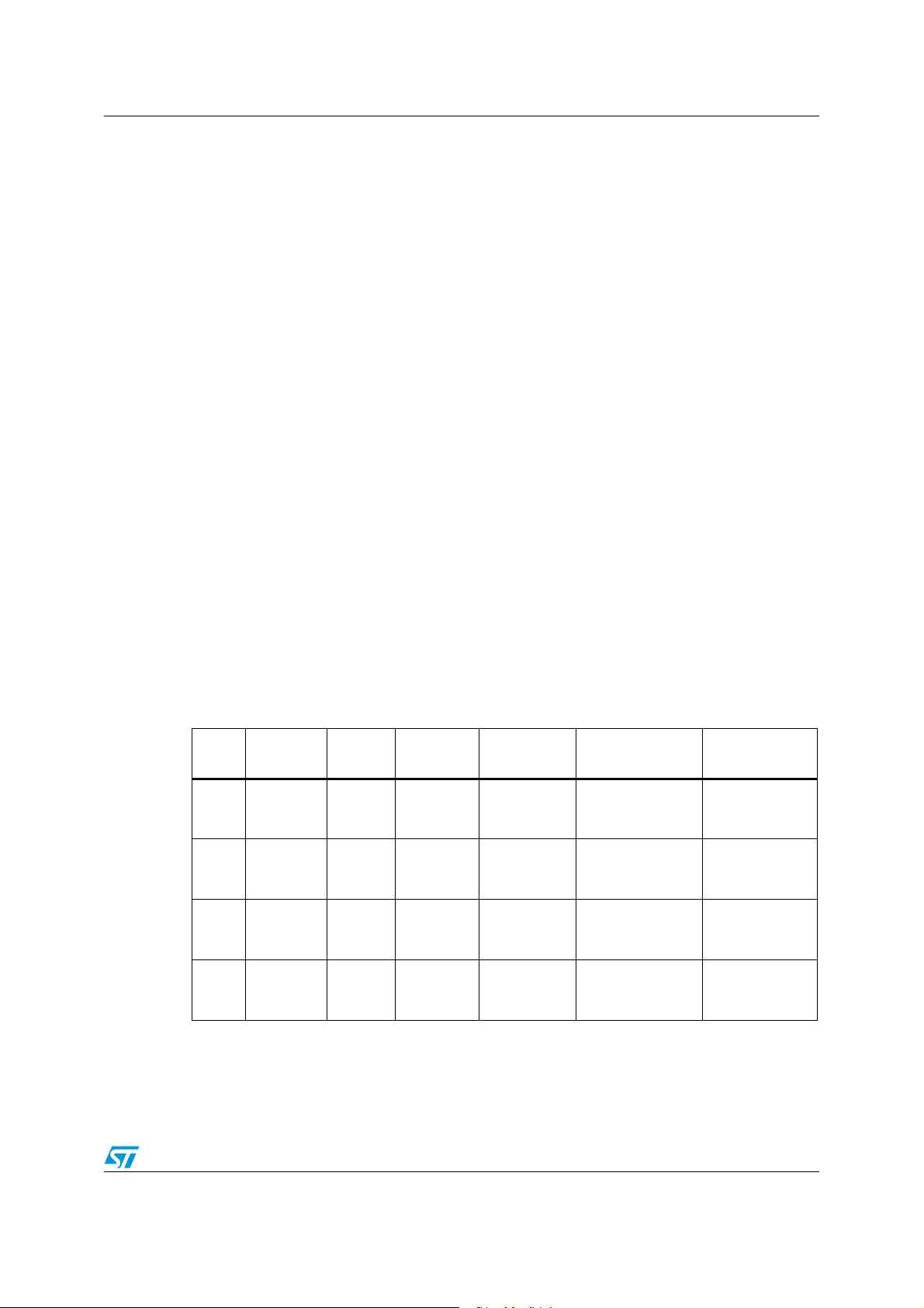
Figure 3. STM32L15xxx UFBGA100 ballout
Doc ID 17659 Rev 6 25/109
Page 26
Pin descriptions STM32L151xx, STM32L152xx
AI16090b
PB2
PC14-
OSC32_IN
PA7PA4
PA2
PA15
PB11
PB1PA6PA3
H
PB10
PC5PC4
D PA8
PA9
BOOT0PB8
C
PC9
PA11
PB6
PC12
V
DDA
PB9
B
PA12
PC10
PC15-
OSC32_OUT
PB3
PD2
A
87654321
V
SS_4
OSC_IN
OSC_OUT V
DD_4
G
F
E
PC2
V
REF+
PC13-
RTC_AF1
PB4 PA13PA14
PB7
PB5
V
SS_3
PC7 PC8PC0NRST PC1
PB0PA5 PB14
V
DD_2
V
DD_3
PB13
VLCD
PC11
PA10
V
SS_2
V
SS_1
PC6V
SSA
PA1
V
DD_1
PB15
PB12
PA0-WKUP1
PH0-
PH1-
-
WKUP2
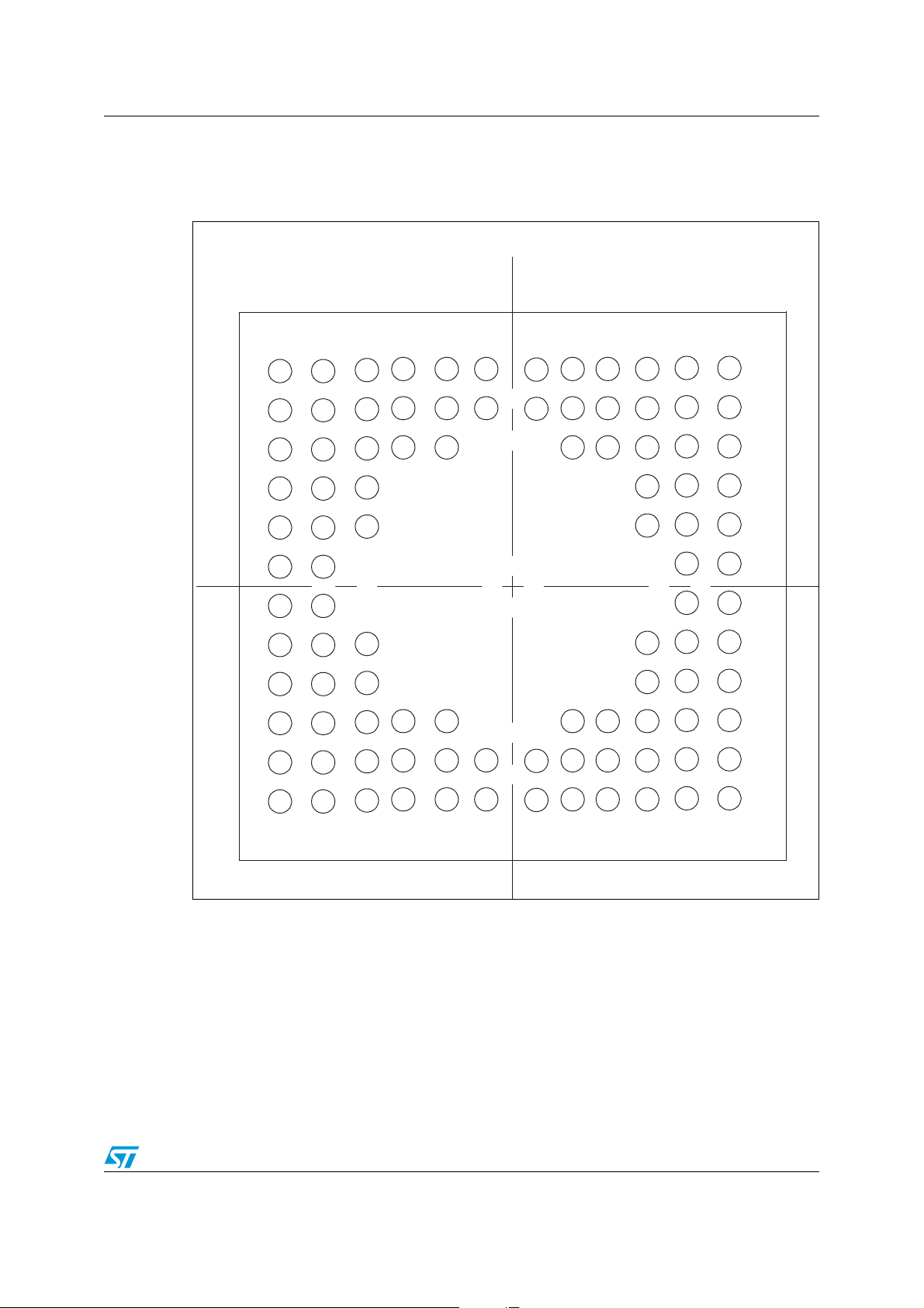
Figure 4. STM32L15xxx TFBGA64 ballout
26/109 Doc ID 17659 Rev 6
Page 27
STM32L151xx, STM32L152xx Pin descriptions
100999897969594939291908988878685848382818079787776
1
2
3
4
5
6
7
8
9
10
11
12
13
14
15
16
17
18
19
20
21
22
23
24
25
75
74
73
72
71
70
69
68
67
66
65
64
63
62
61
60
59
58
57
56
55
54
53
52
51
VDD_2
VSS_2
PH2
PA 1 3
PA 1 2
PA 1 1
PA 1 0
PA 9
PA 8
PC9
PC8
PC7
PC6
PD15
PD14
PD13
PD12
PD11
PD10
PD9
PD8
PB15
PB14
PB13
PB12
PA 3
VSS_4
VDD_4
PA 4
PA 5
PA 6
PA 7
PC4
PC5
PB0
PB1
PB2
PE7
PE8
PE9
PE10
PE11
PE12
PE13
PE14
PE15
PB10
PB11
VSS_1
VDD_1
VDD_3
VSS_3
PE1
PE0
PB9
PB8
BOOT0
PB7
PB6
PB5
PB4
PB3
PD7
PD6
PD5
PD4
PD3
PD2
PD1
PD0
PC12
PC11
PC10
PA15
PA14
26272829303132333435363738394041424344454647484950
PE2
PE3
PE4
PE5
PE6-WKUP3
V
LCD
PC13-RTC_AF1-WKUP2
PC14-OSC32_IN
PC15-OSC32_OUT
VSS_5
VDD_5
PH0-OSC_IN
PH1-OSC_OUT
NRST
PC0
PC1
PC2
PC3
VSSA
VREF-
VREF+
VDDA
PA 0- W K UP1
PA 1
PA 2
ai15692b
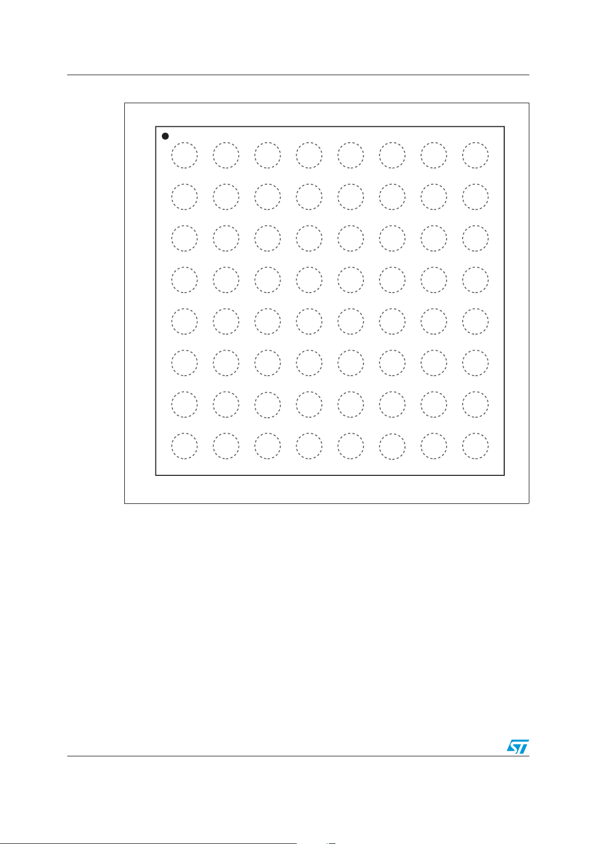
LQFP100
Figure 5. STM32L15xxx LQFP100 pinout
Doc ID 17659 Rev 6 27/109
Page 28
Pin descriptions STM32L151xx, STM32L152xx
44 43 42 41 40 39 38 37
36
35
34
33
32
31
30
29
28
27
26
25
24
23
12
13 14 15 16 17 18 19 20 21 22
1
2
3
4
5
6
7
8
9
10
11
48 47 46 45
PA 3
PA 4
PA 5
PA 6
PA 7
PB0
PB1
PB2
PB10
PB11
VSS_1
VDD_1
VDD_2
VSS_2
PA1 3
PA1 2
PA1 1
PA1 0
PA9
PA8
PB15
PB14
PB13
PB12
V
LCD
PC13- RTC_AF1-WKUP2
PC14-OSC32_IN
PC15-OSC32_OUT
PH0-OSC_IN
PH1-OSC_OUT
NRST
VSSA
VDDA
PA 0 -W K UP1
PA 1
PA 2
VDD_3
VSS_3
PB9
PB8
BOOT0
PB7
PB6
PB5
PB4
PB3
PA1 5
PA 14
LQFP48
ai15694 b
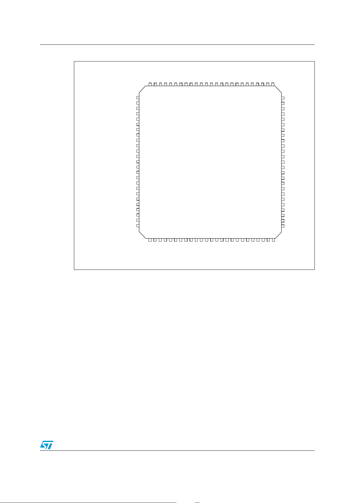
Figure 6. STM32L15xxx LQFP64 pinout
VDD_3
VSS_3
PB9
PB8
BOOT0
PB7
PB6
PB5
PB4
PB3
PD2
PC12
PC11
PC10
PA 1 5
PA 14
V
PC13-RTC_AF1-WKUP2
LCD
PC14-OSC32_IN
PC15-OSC32_OUT
PH0 -OSC_IN
PH1- OSC_OUT
NRST
PC0
PC1
PC2
PC3
VSSA
VDDA
PA 0- W K UP1
PA 1
PA 2
64 63 62 61 60 59 58 57 56 55 54 53 52 51 50 49
1
2
3
4
5
6
7
8
9
10
11
12
13
14
15
16
17 18 19 20 21 22 23 24 29 30 31 3225 26 27 28
PA 3
VSS_4
VDD_4
LQFP64
PA 4
PA 5
PA 6
PA 7
PB0
PB1
PC5
PB2
PB10
PB11
PC4
VDD_2
48
VSS_2
47
PA 1 3
46
PA 1 2
45
PA 1 1
44
PA 1 0
43
PA 9
42
PA 8
41
PC9
40
PC8
39
PC7
38
PC6
37
PB15
36
PB14
35
PB13
34
33
PB12
VSS_1
VDD_1
ai15693b
Figure 7. STM32L15xxx LQFP48 pinout
28/109 Doc ID 17659 Rev 6
Page 29
STM32L151xx, STM32L152xx Pin descriptions
6
33?
"//4
0"
0"
0"
0"
0"
0!
0!
6
$$?
6
33?
0!
5&1&0.
0!
6
33!
0!
6
$$!
0!
0!7+50
0!
0!
0!
0!
6
$$?
0!
0!
0!
0!
0!
0"
0"
0"
6
33?
AIC
0"
0"
0"
0"
0"
0"
6
,#$
0#24#?!&
0#/3#?).
0#/3#?/54
0(/3#?).
0(/3#?/54
.234
0"
0"
6
$$?
Figure 8. STM32L15xxx UFQFPN48 pinout
Doc ID 17659 Rev 6 29/109
Page 30
Pin descriptions STM32L151xx, STM32L152xx
Table 4. STM32L15xxx pin definitions
Pins
(2)
Main
function
(after reset)
I/O Level
(3)
Alternate functions
LQFP100
LQFP64
TFBGA64
Pin name
(1)
Type
UFBGA100
LQFP48 or UFQFPN48
1 - B2 - PE2 I/O FT PE2 TRACECK/LCD_SEG38/TIM3_ETR
2 - A1 - PE3 I/O FT PE3 TRACED0/LCD_SEG39/TIM3_CH1
3 - B1 - PE4 I/O FT PE4 TRACED1/TIM3_CH2
4 - C2 - PE5 I/O FT PE5 TRACED2/TIM9_CH1
5 - D2 - PE6 I/O FT PE6 TRACED3/WKUP3/TIM9_CH2
6 1 B2 E2 1 V
72A2C1 2
83A1D1 3
OSC32_IN
(4)
LCD
PC13-
RTC_AF1
PC14-
SV
LCD
I/O FT PC13 RTC_AF1/WKUP2
I/O PC14 OSC32_IN
(5)
PC15-
9 4 B1 E1 4
OSC32_OUT
(5)
I/O PC15 OSC32_OUT
10 - - F2 - V
11 - - G2 - V
12 5 C1 F1 5
13 6 D1 G1 6
OSC_IN
OSC_OUT
SS_5
DD_5
PH0-
PH1-
SV
SV
I PH0 OSC_IN
(6)
SS_5
DD_5
O PH1 OSC_OUT
14 7 E1 H2 7 NRST I/O NRST
15 8 E3 H1 - PC0 I/O FT PC0 ADC_IN10/LCD_SEG18/ COMP1_INP
16 9 E2 J2 - PC1 I/O FT PC1 ADC_IN11/LCD_SEG19/ COMP1_INP
17 10 F2 J3 - PC2 I/O FT PC2 ADC_IN12/LCD_SEG20/ COMP1_INP
(7)
18 11 -
19 12 F1 J1 8 V
20 - - K1 - V
21 -
22 13 H1 M1 9 V
23 14 G2 L2 10 PA0-WKUP1 I/O FT PA0
K2 - PC3 I/O PC3 ADC_IN13/LCD_SEG21/ COMP1_INP
SV
SV
SV
SV
SSA
REF-
REF+
DDA
G1
L1 - V
(7)
SSA
REF-
REF+
DDA
WKUP1/USART2_CTS/ADC_IN0/TIM2_CH1_ETR/
COMP1_INP
30/109 Doc ID 17659 Rev 6
Page 31

STM32L151xx, STM32L152xx Pin descriptions
Table 4. STM32L15xxx pin definitions (continued)
Pins
(2)
Pin name
(1)
Type
LQFP64
LQFP100
TFBGA64
UFBGA100
LQFP48 or UFQFPN48
24 15 H2 M2 11 PA1 I/O FT PA1
25 16 F3 K3 12 PA2 I/O FT PA2
26 17 G3 L3 13 PA3 I/O PA3
27 18 C2 E3 - V
28 19 D2 H3 - V
SS_4
DD_4
SV
SV
29 20 H3 M3 14 PA4 I/O PA4
30 21 F4 K4 15 PA5 I/O PA5
31 22 G4 L4 16 PA6 I/O FT PA6
32 23 H4 M4 17 PA7 I/O FT PA7
33 24 H5 K5 - PC4 I/O FT PC4 ADC_IN14/LCD_SEG22/COMP1_INP
34 25 H6 L5 - PC5 I/O FT PC5 ADC_IN15/LCD_SEG23/COMP1_INP
35 26 F5 M5 18 PB0 I/O PB0
36 27 G5 M6 19 PB1 I/O FT PB1
37 28 G6 L6 20 PB2 I/O FT PB2/BOOT1
38 - - M7 - PE7 I/O PE7 ADC_IN22/COMP1_INP
39 - - L7 - PE8 I/O PE8 ADC_IN23/COMP1_INP
40 - - M8 - PE9 I/O PE9 ADC_IN24/TIM2_CH1_ETR/COMP1_INP
41 - - L8 - PE10 I/O PE10 ADC_IN25/TIM2_CH2/COMP1_INP
42 - - M9 - PE11 I/O FT PE11 TIM2_CH3
43 - - L9 - PE12 I/O FT PE12 TIM2_CH4/SPI1_NSS
44 - - M10 - PE13 I/O FT PE13 SPI1_SCK
45 - - M11 - PE14 I/O FT PE14 SPI1_MISO
46 - - M12 - PE15 I/O FT PE15 SPI1_MOSI
Main
function
(after reset)
I/O Level
SS_4
DD_4
(3)
Alternate functions
USART2_RTS/ADC_IN1/ TIM2_CH2/LCD_SEG0/
COMP1_INP
USART2_TX/ADC_IN2/ TIM2_CH3/TIM9_CH1/
LCD_SEG1/COMP1_INP
USART2_RX/ADC_IN3/TIM2_CH4/TIM9_CH2/
LCD_SEG2/COMP1_INP
SPI1_NSS/ USART2_CK/
ADC_IN4/DAC_OUT1/COMP1_INP
SPI1_SCK/ADC_IN5/
DAC_OUT2/TIM2_CH1_ETR/COMP1_INP
SPI1_MISO/ADC_IN6/TIM3_CH1/
LCD_SEG3/TIM10_CH1/
COMP1_INP
SPI1_MOSI/ADC_IN7/TIM3_CH2/
LCD_SEG4/TIM11_CH1/COMP1_INP
ADC_IN8/TIM3_CH3/LCD_SEG5/
COMP1_INP/VREF_OUT
ADC_IN9/TIM3_CH4/LCD_SEG6/
COMP1_INP/VREF_OUT
Doc ID 17659 Rev 6 31/109
Page 32

Pin descriptions STM32L151xx, STM32L152xx
Table 4. STM32L15xxx pin definitions (continued)
Pins
(2)
Pin name
(1)
Type
LQFP64
LQFP100
TFBGA64
UFBGA100
LQFP48 or UFQFPN48
47 29 G7 L10 21 PB10 I/O FT PB10 I2C2_SCL/USART3_TX/TIM2_CH3/LCD_SEG10
48 30 H7 L11 22 PB11 I/O FT PB11 I2C2_SDA/ USART3_RX/TIM2_CH4/LCD_SEG11
49 31 D6 F12 23 V
50 32 E6 G12 24 V
SS_1
DD_1
SV
SV
51 33 H8 L12 25 PB12 I/O FT PB12
52 34 G8 K12 26 PB13 I/O FT PB13
53 35 F8 K11 27 PB14 I/O FT PB14
54 36 F7 K10 28 PB15 I/O FT PB15
55 - - K9 - PD8 I/O FT PD8 USART3_TX/LCD_SEG28
56 - - K8 - PD9 I/O FT PD9 USART3_RX/LCD_SEG29
57 - - J12 - PD10 I/O FT PD10 USART3_CK/LCD_SEG30
58 - - J11 - PD11 I/O FT PD11 USART3_CTS/LCD_SEG31
59 - - J10 - PD12 I/O FT PD12
60 - - H12 - PD13 I/O FT PD13 TIM4_CH2/LCD_SEG33
61 - - H11 - PD14 I/O FT PD14 TIM4_CH3/LCD_SEG34
62 - - H10 - PD15 I/O FT PD15 TIM4_CH4/LCD_SEG35
63 37 F6 E12 - PC6 I/O FT PC6 TIM3_CH1/LCD_SEG24
64 38 E7 E11 PC7 I/O FT PC7 TIM3_CH2/LCD_SEG25
65 39 E8 E10 PC8 I/O FT PC8 TIM3_CH3/LCD_SEG26
66 40 D8 D12 - PC9 I/O FT PC9 TIM3_CH4/LCD_SEG27
67 41 D7 D11 29 PA8 I/O FT PA8 USART1_CK/MCO/LCD_COM0
68 42 C7 D10 30 PA9 I/O FT PA9 USART1_TX / LCD_COM1
69 43 C6 C12 31 PA10 I/O FT PA10 USART1_RX / LCD_COM2
70 44 C8 B12 32 PA11 I/O FT PA11 USART1_CTS/ USBDM/SPI1_MISO
71 45 B8 A12 33 PA12 I/O FT PA12 USART1_RTS/USBDP/SPI1_MOSI
72 46 A8 A11 34 PA13 I/O FT JTMS/SWDIO PA13
Main
function
(after reset)
I/O Level
SS_1
DD_1
(3)
Alternate functions
SPI2_NSS/I2C2_SMBA/USART3_CK/LCD_SEG12/
ADC_IN18/COMP1_INP/TIM10_CH1
SPI2_SCK/USART3_CTS/LCD_SEG13/ADC_IN19/
COMP1_INP/TIM9_CH1
SPI2_MISO/ USART3_RTS/LCD_SEG14/ADC_IN20/
COMP1_INP/TIM9_CH2
SPI2_MOSI/LCD_SEG15/ADC_IN21/
COMP1_INP/TIM11_CH1/RTC_50_60Hz
TIM4_CH1 / USART3_RTS/
LCD_SEG32
32/109 Doc ID 17659 Rev 6
Page 33

STM32L151xx, STM32L152xx Pin descriptions
Table 4. STM32L15xxx pin definitions (continued)
Pins
(2)
Pin name
(1)
Type
LQFP64
LQFP100
TFBGA64
UFBGA100
LQFP48 or UFQFPN48
73 - - C11 - PH2 I/O FT PH2 I2C2_SMBA
74 47 D5 F11 35 V
75 48 E5 G11 36 V
SS_2
DD_2
SV
SV
76 49 A7 A10 37 PA14 I/O FT JTCK/SWCLK PA14
77 50 A6 A9 38 PA15 I/O FT JTDI TIM2_CH1_ETR/ PA15/SPI1_NSS/LCD_SEG17
78 51 B7 B11 - PC10 I/O FT PC10
79 52 B6 C10 - PC11 I/O FT PC11 USART3_RX/LCD_SEG29/LCD_SEG41/LCD_COM5
80 53 C5 B10 - PC12 I/O FT PC12 USART3_CK/LCD_SEG30/LCD_SEG42/LCD_COM6
81 - - C9 - PD0 I/O FT PD0 SPI2_NSS/TIM9_CH1
82 - - B9 - PD1 I/O FT PD1 SPI2_SCK
83 54 B5 C8 PD2 I/O FT PD2 TIM3_ETR/LCD_SEG31/LCD_SEG43/LCD_COM7
84 - - B8 - PD3 I/O FT PD3 USART2_CTS/SPI2_MISO
85 - - B7 - PD4 I/O FT PD4 USART2_RTS/SPI2_MOSI
86 - - A6 - PD5 I/O FT PD5 USART2_TX
87 - - B6 - PD6 I/O FT PD6 USART2_RX
88 - - A5 - PD7 I/O FT PD7 USART2_CK/TIM9_CH2
89 55 A5 A8 39 PB3 I/O FT JTDO
90 56 A4 A7 40 PB4 I/O FT JNTRST
91 57 C4 C5 41 PB5 I/O FT PB5
92 58 D3 B5 42 PB6 I/O FT PB6
93 59 C3 B4 43 PB7 I/O FT PB7
94 60 B4 A4 44 BOOT0 I BOOT0
95 61 B3 A3 45 PB8 I/O FT PB8 TIM4_CH3/I2C1_SCL / LCD_SEG16/TIM10_CH1
96 62 A3 B3 46 PB9 I/O FT PB9 TIM4_CH4/I2C1_SDA/LCD_COM3 / TIM11_CH1
97 - - C3 - PE0 I/O FT PE0 TIM4_ETR/LCD_SEG36 /TIM10_CH1
Main
function
(after reset)
I/O Level
SS_2
DD_2
(3)
Alternate functions
USART3_TX/LCD_SEG28/LCD_SEG40/
LCD_COM4
TIM2_CH2 / PB3/TRACESWO
SPI1_SCK/COMP2_INM/LCD_SEG7
TIM3_CH1/ PB4/
SPI1_MISO/COMP2_INP/LCD_SEG8
I2C1_SMBAl/TIM3_CH2
/SPI1_MOSI/COMP2_INP/LCD_SEG9
I2C1_SCL/TIM4_CH1/
USART1_TX
I2C1_SDA/TIM4_CH2/
USART1_RX/PVD_IN
Doc ID 17659 Rev 6 33/109
Page 34

Pin descriptions STM32L151xx, STM32L152xx
Table 4. STM32L15xxx pin definitions (continued)
Pins
(2)
Pin name
(1)
Type
LQFP64
LQFP100
TFBGA64
UFBGA100
LQFP48 or UFQFPN48
98 - - A2 - PE1 I/O FT PE1 LCD_SEG37/TIM11_CH1
99 63 D4 D3 47 V
10
64 E4 C4 48 V
0
1. I = input, O = output, S = supply.
2. FT = 5 V tolerant.
3. Function availability depends on the chosen device. For devices having reduced peripheral counts, it is always the lower
number of peripheral that is included. For example, if a device has only one SPI and two USARTs, they will be called SPI1
and USART1 & USART2, respectively. Refer to Table 2 on page 10.
4. Applicable to STM32L152xx devices only. In STM32L151xx devices, this pin should be connected to V
5. The PC14 and PC15 I/Os are only configured as OSC32_IN/OSC32_OUT when the LSE oscillator is on (by setting the
LSEON bit in the RCC_CSR register). The LSE oscillator pins OSC32_IN/OSC32_OUT can be used as general-purpose
PC14/PC15 I/Os, respectively, when the LSE oscillator is off ( after reset, the LSE oscillator is off ). The LSE has priority
over the GPIO function. For more details, refer to Using the OSC32_IN/OSC32_OUT pins as GPIO PC14/PC15 port pins
section in the STM32L15xxx reference manual (RM0038).
6. The PH0 and PH1 I/Os are only configured as OSC_IN/OSC_OUT when the HSE oscillator is on ( by setting the HSEON bit
in the RCC_CR register). The HSE oscillator pins OSC_IN/OSC_OUT can be used as general-purpose PH0/PH1 I/Os,
respectively, when the HSE oscillator is off (after reset, the HSE oscillator is off ). The HSE has priority over the GPIO
function.
7. Unlike in the LQFP64 package, there is no PC3 in the TFBGA64 package. The V
SS_3
DD_3
SV
SV
Main
function
(after reset)
I/O Level
SS_3
DD_3
(3)
Alternate functions
.
DD
functionality is provided instead.
REF+
34/109 Doc ID 17659 Rev 6
Page 35

Table 5. Alternate function input/output
STM32L151xx, STM32L152xx Pin descriptions
Digital alternate function number
Port
name
BOOT0 BOOT0
NRST NRST
PA0-WKUP1 WKUP1
PA1 TIM2_CH2
Doc ID 17659 Rev 6 35/109
PA2 TIM2_CH3 TIM9_CH1
PA3 TIM2_CH4 TIM9_CH2
PA 4 SPI1_NSS
PA 5
PA6 TIM3_CH1 TIM10_CH1 SPI1_MISO [SEG3] TIMx_IC3 EVENTOUT
PA7 TIM3_CH2 TIM11_CH1 SPI1_MOSI [SEG4] TIMx_IC4 EVENTOUT
PA 8 M CO
PA 9
PA 10
PA 11 SPI1_MISO
PA 12 SPI1_MOSI
PA13 JTMS-SWDAT TIMx_IC2 EVENTOUT
PA14 JTCK-SWCLK TIMx_IC3 EVENTOUT
AFIO0 AFIO1 AFIO2 AFIO3 AFIO4 AFIO5 AFOI6 AFIO7 AFIO8 AFIO9 AFIO10 AFIO11 AFIO12 AFIO13 AFIO14 AFIO15
Alternate function
SYSTEM TIM2 TIM3/4 TIM9/10/11 I2C1/2 SPI1/2 N/A
TIM2_CH1_
ETR
TIM2_CH1_
ETR
SPI1_SCK TIMx_IC2 EVENTOUT
USART
1/2/3
USART2_
CTS
USART2_
RTS
USART2_
TX
USART2_
RX
USART2_
CK
USART1_
CK
USART1_
TX
USART1_
RX
USART1_
CTS
USART1_
RTS
N/A N/A USBFS LCD N/A N/A RI SYSTEM
TIMx_IC1 EVENTOUT
[SEG0] TIMx_IC2 EVENTOUT
[SEG1] TIMx_IC3 EVENTOUT
[SEG2] TIMx_IC4 EVENTOUT
TIMx_IC1 EVENTOUT
[COM0] TIMx_IC1 EVENTOUT
[COM1] TIMx_IC2 EVENTOUT
[COM2] TIMx_IC3 EVENTOUT
DM TIMx_IC4 EVENTOUT
DP TIMx_IC1 EVENTOUT
Page 36

36/109 Doc ID 17659 Rev 6
Table 5. Alternate function input/output (continued)
Pin descriptions STM32L151xx, STM32L152xx
Digital alternate function number
Port
name
PA15 JTDI
PB0 TIM3_CH3 [SEG5] EVENTOUT
PB1 TIM3_CH4 [SEG6] EVENTOUT
PB2 BOOT1 EVENTOUT
PB3 JTDO TIM2_CH2 SPI1_SCK [SEG7] EVENTOUT
PB4 JTRST TIM3_CH1 SPI1_MISO [SEG8] EVENTOUT
PB5 TIM3_CH2
PB6 TIM4_CH1 I2C1_SCL
PB7 TIM4_CH2 I2C1_SDA
PB8 TIM4_CH3
PB9 TIM4_CH4
PB10 TIM2_CH3 I2C2_SCL
PB11 TIM2_CH4 I2C2_SDA
PB12 TIM10_CH1
PB13 TIM9_CH1 SPI2_SCK
PB14 TIM9_CH2 SPI2_MISO
PB15 RTC 50/60 Hz TIM11_CH1 SPI2_MOSI SEG15 EVENTOUT
PC0 SEG18 TIMx_IC1 EVENTOUT
AFIO0 AFIO1 AFIO2 AFIO3 AFIO4 AFIO5 AFOI6 AFIO7 AFIO8 AFIO9 AFIO10 AFIO11 AFIO12 AFIO13 AFIO14 AFIO15
Alternate function
SYSTEM TIM2 TIM3/4 TIM9/10/11 I2C1/2 SPI1/2 N/A
TIM2_CH1_
ETR
TIM10_CH1
*
TIM11_CH1
*
I2C1_SMB
Al
I2C1_SCL SEG16 EVENTOUT
I2C1_SDA [COM3] EVENTOUT
I2C2_SMB
Al
SPI1_NSS SEG17 TIMx_IC4 EVENTOUT
SPI1_MOSI [SEG9] EVENTOUT
SPI2_NSS
USART
1/2/3
USART1_
TX
USART1_
RX
USART3_
TX
USART3_
RX
USART3_
CK
USART3_
CTS
USART3_
RTS
N/A N/A USBFS LCD N/A N/A RI SYSTEM
EVENTOUT
EVENTOUT
SEG10 EVENTOUT
SEG11 EVENTOUT
SEG12 EVENTOUT
SEG13 EVENTOUT
SEG14 EVENTOUT
Page 37

Table 5. Alternate function input/output (continued)
STM32L151xx, STM32L152xx Pin descriptions
Digital alternate function number
Port
name
PC1 SEG19 TIMx_IC2 EVENTOUT
PC2 SEG20 TIMx_IC3 EVENTOUT
PC3 SEG21 TIMx_IC4 EVENTOUT
PC4 SEG22 TIMx_IC1 EVENTOUT
PC5 SEG23 TIMx_IC2 EVENTOUT
PC6 TIM3_CH1 SEG24 TIMx_IC3 EVENTOUT
Doc ID 17659 Rev 6 37/109
PC7 TIM3_CH2 SEG25 TIMx_IC4 EVENTOUT
PC8 TIM3_CH3 SEG26 TIMx_IC1 EVENTOUT
PC9 TIM3_CH4 SEG27 TIMx_IC2 EVENTOUT
PC10
PC11
PC12
AFIO0 AFIO1 AFIO2 AFIO3 AFIO4 AFIO5 AFOI6 AFIO7 AFIO8 AFIO9 AFIO10 AFIO11 AFIO12 AFIO13 AFIO14 AFIO15
Alternate function
SYSTEM TIM2 TIM3/4 TIM9/10/11 I2C1/2 SPI1/2 N/A
USART
1/2/3
USART3_
TX
USART3_
RX
USART3_
CK
N/A N/A USBFS LCD N/A N/A RI SYSTEM
COM4 /
SEG28 /
SEG40
COM5 /
SEG29 /
SEG41
COM6 /
SEG30 /
SEG42
TIMx_IC3 EVENTOUT
TIMx_IC4 EVENTOUT
TIMx_IC1 EVENTOUT
PC13RTC_AF1
PC14OSC32_IN
PC15OSC32_OUT
PD0 TIM9_CH1 SPI2_NSS TIMx_IC1 EVENTOUT
PD1 SPI2_SCK TIMx_IC2 EVENTOUT
RTC_AF1 /
WKUP2
OSC32_IN TIMx_IC3 EVENTOUT
OSC32_OUT TIMx_IC4 EVENTOUT
TIMx_IC2 EVENTOUT
Page 38

38/109 Doc ID 17659 Rev 6
Table 5. Alternate function input/output (continued)
Pin descriptions STM32L151xx, STM32L152xx
Digital alternate function number
Port
name
PD2 TIM3_ETR
PD3 SPI2_MISO
PD4 SPI2_MOSI
PD5
PD6
PD7 TIM9_CH2
PD8
PD9
PD10
PD11
PD12 TIM4_CH1
PD13 TIM4_CH2 SEG33 TIMx_IC2 EVENTOUT
PD14 TIM4_CH3 SEG34 TIMx_IC3 EVENTOUT
PD15 TIM4_CH4 SEG35 TIMx_IC4 EVENTOUT
PE0 TIM4_ETR TIM10_CH1 SEG36 TIMx_IC1 EVENTOUT
PE1 TIM11_CH1 SEG37 TIMx_IC2 EVENTOUT
PE2 TRACECK TIM3_ETR SEG 38 TIMx_IC3 EVENTOUT
PE3 TRACED0 TIM3_CH1 SEG 39 TIMx_IC4 EVENTOUT
AFIO0 AFIO1 AFIO2 AFIO3 AFIO4 AFIO5 AFOI6 AFIO7 AFIO8 AFIO9 AFIO10 AFIO11 AFIO12 AFIO13 AFIO14 AFIO15
Alternate function
SYSTEM TIM2 TIM3/4 TIM9/10/11 I2C1/2 SPI1/2 N/A
USART
1/2/3
USART2_
CTS
USART2_
RTS
USART2_
TX
USART2_
RX
USART2_
CK
USART3_
TX
USART3_
RX
USART3_
CK
USART3_
CTS
USART3_
RTS
N/A N/A USBFS LCD N/A N/A RI SYSTEM
COM7 /
SEG31 /
SEG43
SEG28 TIMx_IC1 EVENTOUT
SEG29 TIMx_IC2 EVENTOUT
SEG30 TIMx_IC3 EVENTOUT
SEG31 TIMx_IC4 EVENTOUT
SEG32 TIMx_IC1 EVENTOUT
TIMx_IC3 EVENTOUT
TIMx_IC4 EVENTOUT
TIMx_IC1 EVENTOUT
TIMx_IC2 EVENTOUT
TIMx_IC3 EVENTOUT
TIMx_IC4 EVENTOUT
Page 39

Table 5. Alternate function input/output (continued)
STM32L151xx, STM32L152xx Pin descriptions
Digital alternate function number
Port
name
PE4 TRACED1 TIM3_CH2 TIMx_IC1 EVENTOUT
PE5 TRACED2 TIM9_CH1* TIMx_IC2 EVENTOUT
PE6
PE7 TIMx_IC4 EVENTOUT
PE8 TIMx_IC1 EVENTOUT
Doc ID 17659 Rev 6 39/109
PE9
PE10 TIM2_CH2 TIMx_IC3 EVENTOUT
PE11 TIM2_CH3 TIMx_IC4 EVENTOUT
PE12 TIM2_CH4 SPI1_NSS TIMx_IC1 EVENTOUT
PE13 SPI1_SCK TIMx_IC2 EVENTOUT
PE14 SPI1_MISO TIMx_IC3 EVENTOUT
PE15 SPI1_MOSI TIMx_IC4 EVENTOUT
PH0-OSC_IN OSC_IN
PH1OSC_OUT
PH2
AFIO0 AFIO1 AFIO2 AFIO3 AFIO4 AFIO5 AFOI6 AFIO7 AFIO8 AFIO9 AFIO10 AFIO11 AFIO12 AFIO13 AFIO14 AFIO15
Alternate function
SYSTEM TIM2 TIM3/4 TIM9/10/11 I2C1/2 SPI1/2 N/A
TRACED3 /
WKUP3
OSC_OUT
TIM2_CH1_
ETR
TIM9_CH2* TIMx_IC3 EVENTOUT
USART
1/2/3
N/A N/A USBFS LCD N/A N/A RI SYSTEM
TIMx_IC2 EVENTOUT
Page 40
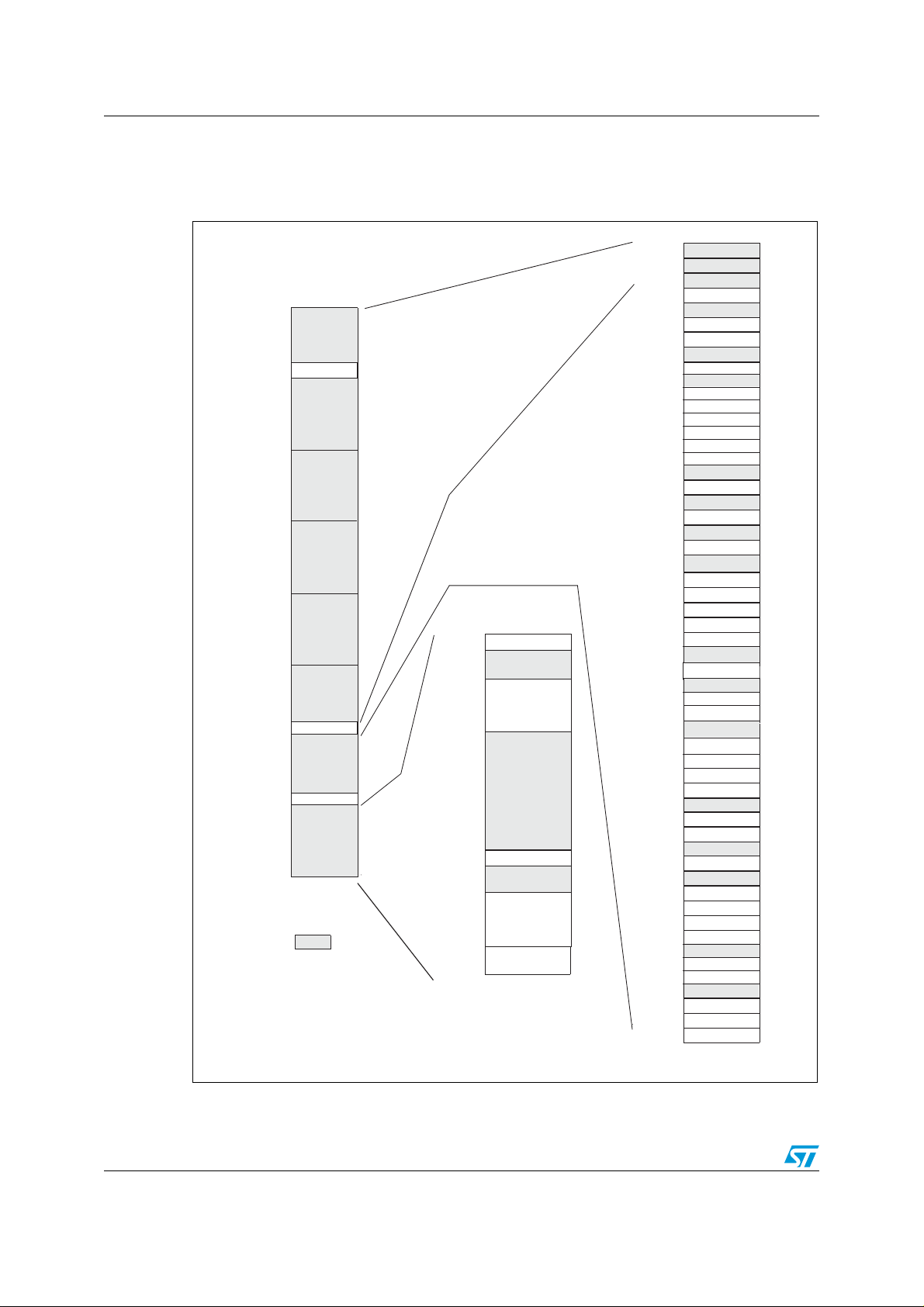
reserved
0x4000 0000
0x4000 0400
0x4000 0800
0x4000 0C00
0x4000 2800
0x4000 2C00
0x4000 3000
0x4000 3400
0x4000 3800
0x4000 3C00
0x4000 4400
0x4000 4800
0x4000 4C00
0x4001 0C00
0x4001 1000
0x4001 1400
APB memory space
CRC
0x4002 3800
TIM2
Reserved
0x4001 0800
0x4001 2400
0x4001 2800
0x4001 3000
0x4001 3400
0x4001 3800
TIM3
TIM4
RTC
WWDG
IWDG
reserved
SPI2
USART2
USART3
SYSCFG
TIM9
TIM11
reserve d
ADC
reserved
USART1
reserved
0x4002 3400
0x4002 0000
0x4001 3C00
0x4000 5400
0x4000 5800
reserved
reserved
SPI1
I2C1
0x4000 6000
0x4000 5C00
PWR
TIM10
I2C2
reserved
EXTI
reserved
RCC
Flash In terface
reserved
reserved
reserved
0x4000 6200
0x4000 7000
0x4000 7400
0x4000 7C00
0x4001 0400
0x4002 3C00
0x4002 4000
0x4002 6000
0x4002 6400
0x6000 0000
0xE010 0000
reserved
0xFFFF FFFF
USB Regi sters
DMA
0
1
2
3
4
5
6
7
0x2000 0000
0x4000 0000
0x6000 0000
0x8000 0000
0xA000 0000
0xC000 0000
0xE000 0000
0xFFFF FFFF
0x0000 0000
Peripherals
SRAM
Cortex- M3 Internal
Perip herals
0xE010 0000
ai18200b
512 byte
USB
TIM6
TIM7
LCD
reserved
reserved
0x4000 1000
0x4000 1400
0x4000 2400
0x4000 1C00
DAC1 & 2
0x4000 7800
Port A
Port B
Port C
Port D
Port E
Port H
reserved
0x4002 3000
0x4002 1800
0x4002 1400
0x4002 1000
0x4002 0C00
0x4002 0800
0x4002 0400
COMP + RI
Flash memory
reserved
reserved
0x0800 0000
0x0801 FFFF
0x1FF0 0000
0x1FF8 001F
System memory
Option Bytes
0x1FF0 0FFF
0x1FF8 0000
Aliased to Flash or system
memory depending on
BOOT pins
0x0000 0000
reserved
Data EEPROM
reserved
0x0808 0000
0x0808 0FFF
0x4001 0000
reserved
reserved
Memory mapping STM32L151xx, STM32L152xx
5 Memory mapping
The memory map is shown in the following figure.Figure 9.Memory map
40/109 Doc ID 17659 Rev 6
Page 41

STM32L151xx, STM32L152xx Electrical characteristics
AI
#P&
34-,XXXPIN
AI
34-,XXXPIN
6
).
6 Electrical characteristics
6.1 Parameter conditions
Unless otherwise specified, all voltages are referenced to VSS.
6.1.1 Minimum and maximum values
Unless otherwise specified the minimum and maximum values are guaranteed in the worst
conditions of ambient temperature, supply voltage and frequencies by tests in production on
100% of the devices with an ambient temperature at T
the selected temperature range).
Data based on characterization results, design simulation and/or technology characteristics
are indicated in the table footnotes and are not tested in production. Based on
characterization, the minimum and maximum values refer to sample tests and represent the
mean value plus or minus three times the standard deviation (mean±3
6.1.2 Typical values
Unless otherwise specified, typical data are based on TA = 25 °C, VDD = 3.6 V (for the
1.65
V ≤ V
tested.
≤ 3.6 V voltage range). They are given only as design guidelines and are not
DD
= 25 °C and TA = TAmax (given by
A
Σ).
Typical ADC accuracy values are determined by characterization of a batch of samples from
a standard diffusion lot over the full temperature range, where 95% of the devices have an
error less than or equal to the value indicated
6.1.3 Typical curves
Unless otherwise specified, all typical curves are given only as design guidelines and are
not tested.
6.1.4 Loading capacitor
The loading conditions used for pin parameter measurement are shown in Figure 10.
6.1.5 Pin input voltage
The input voltage measurement on a pin of the device is described in Figure 11.
Figure 10. Pin loading conditions Figure 11. Pin input voltage
(mean±2Σ).
Doc ID 17659 Rev 6 41/109
Page 42

Electrical characteristics STM32L151xx, STM32L152xx
ai15401c
V
DD1/2/.../5
Analo g:
RCs, PLL,
...
GP I/O s
OUT
IN
Kernel logic
(CPU,
Digital
& Memories)
Standby-power circuitry
(OSC32K,RTC,
RTC backup registers)
Wake-up logic
11 × 100 nF
+ 1 × 4.7 µF
Regulator
V
SS1/2/.../5
V
DDA
V
REF+
V
REF-
V
SSA
ADC
Level shifter
IO
Logic
V
DD
10 nF
+ 1 µF
V
REF
10 nF
+ 1 µF
V
DD
ai14126b
V
DD
V
DDA
I
DD
6.1.6 Power supply scheme
Figure 12. Power supply scheme
Caution: In this figure, the 4.7 µF capacitor must be connected to V
6.1.7 Current consumption measurement
Figure 13. Current consumption measurement scheme
42/109 Doc ID 17659 Rev 6
DD2
.
Page 43

STM32L151xx, STM32L152xx Electrical characteristics
6.2 Absolute maximum ratings
Stresses above the absolute maximum ratings listed in Tab le 6: Voltage characteristics,
Ta bl e 7: Current characteristics, and Ta bl e 8: Thermal characteristics may cause permanent
damage to the device. These are stress ratings only and functional operation of the device
at these conditions is not implied. Exposure to maximum rating conditions for extended
periods may affect device reliability.
Table 6. Voltage characteristics
Symbol Ratings Min Max Unit
VDD–V
(2)
V
IN
|ΔV
DDx
− VSS| Variations between all different ground pins 50
|V
SSX
V
ESD(HBM)
1. All main power (VDD, V
supply, in the permitted range.
2. V
maximum must always be respected. Refer to Table 7 for maximum allowed injected current values.
IN
Table 7. Current characteristics
External main supply voltage
SS
(including V
DDA
and VDD)
(1)
Input voltage on five-volt tolerant pin V
Input voltage on any other pin V
| Variations between different V
power pins 50
DD
Electrostatic discharge voltage
(human body model)
) and ground (VSS, V
DDA
) pins must always be connected to the external power
SSA
–0.3 4.0
− 0.3 VDD+4.0
SS
− 0.3 4.0
SS
see Section 6.3.10
Symbol Ratings Max. Unit
(1)
(1)
80
80
I
VDD
I
VSS
Total current into VDD/V
Total current out of V
SS
power lines (source)
DDA
ground lines (sink)
Output current sunk by any I/O and control pin 25
I
IO
I
INJ(PIN)
ΣI
INJ(PIN)
1. All main power (VDD, V
supply, in the permitted range.
2. Negative injection disturbs the analog performance of the device. See note in Section 6.3.16.
3. Positive current injection is not possible on these I/Os. A negative injection is induced by VIN<VSS. I
must never be exceeded. Refer to Table 6 for maximum allowed input voltage values.
4. A positive injection is induced by V
must never be exceeded. Refer to Table 6: Voltage characteristics for the maximum allowed input voltage
values.
5. When several inputs are submitted to a current injection, the maximum ΣI
positive and negative injected currents (instantaneous values).
Output current sourced by any I/O and control pin - 25
Injected current on five-volt tolerant I/O
(2)
Injected current on any other pin
(3)
(4)
Total injected current (sum of all I/O and control pins)
) and ground (VSS, V
DDA
> VDD while a negative injection is induced by V
IN
) pins must always be connected to the external power
SSA
INJ(PIN)
+0 /-5
± 5
(5)
is the absolute sum of the
< VSS. I
IN
± 25
INJ(PIN)
mA
INJ(PIN)
V
mV
Doc ID 17659 Rev 6 43/109
Page 44

Electrical characteristics STM32L151xx, STM32L152xx
Table 8. Thermal characteristics
Symbol Ratings Value Unit
T
STG
T
J
Storage temperature range –65 to +150 °C
Maximum junction temperature 150 °C
6.3 Operating conditions
6.3.1 General operating conditions
Table 9. General operating conditions
Symbol Parameter Conditions Min Max Unit
f
HCLK
PCLK1
f
PCLK2
V
DD
V
DDA
P
A Temperature range
T
Internal AHB clock frequency 0 32
Internal APB1 clock frequency 0 32
Internal APB2 clock frequency 0 32
Standard operating voltage
Analog operating voltage
(ADC and DAC not used)
(1)
Analog operating voltage
(ADC or DAC used)
Power dissipation at
D
= 85 °C
T
A
(3)
BOR detector disabled 1.65 3.6
BOR detector enabled,
at power on
BOR detector disabled,
after power on
1.8 3.6
1.65 3.6
1.65 3.6
Must be the same voltage
(2)
as V
DD
1.8 3.6
290 mW
Maximum power dissipation –40 85
Low power dissipation
(4)
–40 105
MHzf
V
V
°C
T
J Junction temperature range -40 °C ≤ TA ≤ 105 °C –40 105 °C
1. When the ADC is used, refer to Table 50: ADC characteristics.
2. It is recommended to power VDD and V
between V
3. If TA is lower, higher PD values are allowed as long as TJ does not exceed TJ max (see Table 64: Thermal
characteristics on page 104).
4. In low power dissipation state, TA can be extended to this range as long as TJ does not exceed TJ max
(see Table 64: Thermal characteristics on page 104).
DD
and V
can be tolerated during power-up and operation.
DDA
from the same source. A maximum difference of 300 mV
DDA
44/109 Doc ID 17659 Rev 6
Page 45

STM32L151xx, STM32L152xx Electrical characteristics
Table 10. Functionalities depending on the operating power supply range
Functionalities depending on the operating power supply range
Maximum
Operating power
supply range
= 1.65 to 1.8 V Not functional
V
DD
= 1.8 to 2.0 V
V
DD
DAC and ADC
operation
Conversion
time up to 500
Ksps
USB V
Not
functional
Not
functional
CORE
Range 2 or
range 3
Range 2 or
range 3
CPU
frequency
max)
(f
CPU
16 MHz
(1ws)
8MHz
(0ws)
16 MHz
(1ws)
8MHz
(0ws)
I/O operation
- Degraded speed
performance
- Degraded speed
performance
Conversion
= 2.0 to 2.4 V
V
DD
time up to 500
Functional
Ksps
Conversion
= 2.4 to 3.6 V
V
DD
time up to 1
Functional
Msps
1. Should be USB compliant from I/O voltage standpoint, the minimum VDD is 3.0 V.
Range 1, range
(1)
2 or range 3
Range 1, range
(1)
2 or range 3
32 MHz
(1ws)
16MHz
(0ws)
32 MHz
(1ws)
16MHz
(0ws)
- Full speed operation
- Full speed operation
Doc ID 17659 Rev 6 45/109
Page 46

Electrical characteristics STM32L151xx, STM32L152xx
6.3.2 Embedded reset and power control block characteristics
The parameters given in the following table are derived from the tests performed under the
ambient temperature condition summarized in
Table 11. Embedded reset and power control block characteristics
Symbol Parameter Conditions Min Typ Max Unit
Ta bl e 9.
t
VDD
T
RSTTEMPO
V
POR/PDR
V
BOR0
V
BOR1
V
BOR2
V
BOR3
V
BOR4
V
PVD0
V
PVD1
V
PVD2
VDD rise time rate
(1)
V
fall time rate
DD
(1)
Reset temporization
Power on/power down reset
threshold
Brown-out reset threshold 0
Brown-out reset threshold 1
Brown-out reset threshold 2
Brown-out reset threshold 3
Brown-out reset threshold 4
Programmable voltage detector
threshold 0
PVD threshold 1
PVD threshold 2
BOR detector enabled 0
BOR detector disabled 0
BOR detector enabled 20
BOR detector disabled 0
∞
1000
∞
1000
VDD rising, BOR enabled 2 3.3
rising, BOR disabled 0.4 0.7 1.6
V
DD
Falling edge 1 1.5 1.65
Rising edge 1.3 1.5 1.65
Falling edge 1.67 1.7 1.74
Rising edge 1.69 1.76 1.8
Falling edge 1.87 1.93 1.97
Rising edge 1.96 2.03 2.07
Falling edge 2.22 2.30 2.35
Rising edge 2.31 2.41 2.44
Falling edge 2.45 2.55 2.60
Rising edge 2.54 2.66 2.7
Falling edge 2.68 2.8 2.85
Rising edge 2.78 2.9 2.95
Falling edge 1.8 1.85 1.88
Rising edge 1.88 1.94 1.99
Falling edge 1.98 2.04 2.09
Rising edge 2.08 2.14 2.18
Falling edge 2.20 2.24 2.28
Rising edge 2.28 2.34 2.38
µs/V
ms
V
V
PVD3
PVD threshold 3
Rising edge 2.47 2.54 2.58
Falling edge 2.57 2.64 2.69
Falling edge 2.39 2.44 2.48
V
PVD4
PVD threshold 4
Rising edge 2.68 2.74 2.79
Falling edge 2.77 2.83 2.88
V
PVD5
PVD threshold 5
Rising edge 2.87 2.94 2.99
46/109 Doc ID 17659 Rev 6
Page 47

STM32L151xx, STM32L152xx Electrical characteristics
Table 11. Embedded reset and power control block characteristics (continued)
Symbol Parameter Conditions Min Typ Max Unit
V
PVD6
V
hyst
1. Guaranteed by characterisation, not tested in production.
PVD threshold 6
Hysteresis voltage
Falling edge 2.97 3.05 3.09
Rising edge 3.08 3.15 3.20
BOR0 threshold 40
All BOR and PVD thresholds
excepting BOR0
100
V
mV
Doc ID 17659 Rev 6 47/109
Page 48

Electrical characteristics STM32L151xx, STM32L152xx
6.3.3 Embedded internal reference voltage
The parameters given in Tab l e 12 are based on characterization results, unless otherwise
specified.
Coeff
Coeff
(3)
(3)
(3)(4)
(3)
Typ
(1)
Internal reference voltage – 40 °C < TJ < +105 °C 1.202 1.224 1.242 V
Internal reference current
consumption
1.4 2.3 µA
Internal reference startup time 2 3 ms
V
and V
DDA
V
factory measure
REFINT
Accuracy of factory-measured
V
value
REF
voltage during
REF+
(2)
Including uncertainties
due to ADC and
V
DDA/VREF+
values
2.99 3 3.01 V
–40 °C < TJ < +105 °C 20 50
Temperature coefficient
0 °C < T
< +50 °C 20
J
Long-term stability 1000 hours, T= 25 °C 1000 ppm
(3)
Voltage coefficient 3.0 V < V
< 3.6 V 2000 ppm/V
DDA
ADC sampling time when
reading the internal reference
510 µs
voltage
Startup time of reference voltage
buffer for ADC
Max Unit
±5 mV
ppm/°C
10 µs
Table 12. Embedded internal reference voltage
Symbol Parameter Conditions Min
V
REFINT out
I
REFINT
T
VREFINT
V
VREF_MEAS
A
VREF_MEAS
T
A
VDDCoeff
T
S_vrefint
T
ADC_BUF
Consumption of reference
LPBUF
(3)
(3)
voltage buffer for ADC
(3)
VREF_OUT output current
(3)
VREF_OUT output load 50 pF
(5)
Consumption of reference
voltage buffer for VREF_OUT
I
BUF_ADC
I
VREF_OUT
C
VREF_OUT
I
and COMP
V
REFINT_DIV1
V
REFINT_DIV2
V
REFINT_DIV3
1. Tested in production;
2. The internal V
3. Guaranteed by design, not tested in production.
4. Shortest sampling time can be determined in the application by multiple iterations.
5. To guarantee less than 1% VREF_OUT deviation.
(3)
1/4 reference voltage 24 25 26
(3)
1/2 reference voltage 49 50 51
(3)
3/4 reference voltage 74 75 76
value is individually measured in production and stored in dedicated EEPROM bytes.
REF
13.5 25 µA
1µA
730 1200 nA
%
V
REFINT
48/109 Doc ID 17659 Rev 6
Page 49

STM32L151xx, STM32L152xx Electrical characteristics
6.3.4 Supply current characteristics
The current consumption is a function of several parameters and factors such as the
operating voltage, ambient temperature, I/O pin loading, device software configuration,
operating frequencies, I/O pin switching rate, program location in memory and executed
binary code. The current consumption is measured as described in
consumption measurement scheme.
All Run-mode current consumption measurements given in this section are performed with a
reduced code that gives a consumption equivalent to Dhrystone 2.1 code.
Maximum current consumption
The MCU is placed under the following conditions:
● V
● All I/O pins are in input mode with a static value at V
● All peripherals are disabled except when explicitly mentioned
● The Flash memory access time is adjusted depending on f
● Prefetch and 64-bit access are enabled in configurations with 1 wait state
The parameters given in Tab l e 13, Ta bl e 9 and Ta bl e 11 are derived from tests performed
under ambient temperature and VDD supply voltage conditions summarized in Ta bl e 9.
Table 13. Current consumption in Run mode, code with data processing running from Flash
Symbol Parameter
DD
range
= 3.6 V
Conditions
f
HCLK
or VSS (no load)
DD
Typ
Figure 13: Current
frequency and voltage
HCLK
(1)
Max
55 °C 85 °C 105 °C
Unit
1 MHz 270 400 400 400
4 MHz 890 1025 1025 1025
4 MHz 1 1.3 1.3 1.3
8 MHz 2 2.5 2.5 2.5
16 MHz 3.9 5 5 5
8 MHz 2.16 3 3 3
16 MHz 4.8 5.5 5.5 5.5
32 MHz 9.6 11 11 11
16 MHz 4 5 5 5
32 MHz 9.4 11 11 11
I
DD (Run
from
Flash)
Supply
current in
Run mode,
code
executed
from Flash
f
HSE
= f
HCLK
up to 8 MHz,
included
= f
f
HSE
above 8 MHz
(PLL ON)
HCLK
(2)
/2
HSI clock source
(16 MHz)
Range 3,
V
=1.2 V
CORE
VOS[1:0] = 11
Range 2,
V
=1.5 V
CORE
VOS[1:0] = 10
Range 1,
V
=1.8 V
CORE
VOS[1:0] = 01
Range 2,
V
=1.5 V
CORE
VOS[1:0] = 10
Range 1,
V
=1.8 V
CORE
VOS[1:0] = 01
MSI clock, 65 kHz
MSI clock, 524 kHz 524 kHz 0.15 0.185 0.19 0.2
MSI clock,
1. Based on characterization, not tested in production, unless otherwise specified.
2. Oscillator bypassed (HSEBYP = 1 in RCC_CR register).
4.2 MHz 4.2 MHz 0.9 1 1 1
Range 3,
V
=1.2 V
CORE
VOS[1:0] = 11
65 kHz 0.05 0.085 0.09 0.1
µA2 MHz 470 600 600 600
mA
Doc ID 17659 Rev 6 49/109
Page 50

Electrical characteristics STM32L151xx, STM32L152xx
Table 14. Current consumption in Run mode, code with data processing running from RAM
Symbol Parameter Conditions f
I
DD (Run
from
RAM)
Supply current
in Run mode,
code executed
from RAM,
Flash switched
off
f
HSE
= f
HCLK
up to 8 MHz,
included
= f
f
HSE
above 8 MHz
(PLL ON)
HCLK
(2)
/2
HSI clock source
(16 MHz)
Range 3,
V
=1.2 V
CORE
VOS[1:0] = 11
Range 2,
V
=1.5 V
CORE
VOS[1:0] = 10
Range 1,
=1.8 V
V
CORE
VOS[1:0] = 01
Range 2,
V
=1.5 V
CORE
VOS[1:0] = 10
Range 1,
=1.8 V
V
CORE
(1)
Max
HCLK
Typ
55 °C 85 °C 105 °C
1 MHz 200 300 300 300
4 MHz 720 860 860 860
4 MHz 0.9 1 1 1
8 MHz 1.65 2 2 2
16 MHz 3.2 3.7 3.7 3.7
8 MHz 2 2.5 2.5 2.5
16 MHz 4 4.5 4.5 4.5
32 MHz 7.7 8.5 8.5 8.5
16 MHz 3.3 3.8 3.8 3.8
32 MHz 7.8 9.2 9.2 9.2
(3)
VOS[1:0] = 01
MSI clock, 65 kHz
MSI clock, 4.2 MHz 4.2 MHz 700 800 800 820
1. Based on characterization, not tested in production, unless otherwise specified.
2. Oscillator bypassed (HSEBYP = 1 in RCC_CR register).
3. Tested in production.
Range 3,
V
=1.2 V
CORE
VOS[1:0] = 11
65 kHz 40 60 60 80
Unit
µA2 MHz 380 500 500 500
mA
µAMSI clock, 524 kHz 524 kHz 110 140 140 160
50/109 Doc ID 17659 Rev 6
Page 51

STM32L151xx, STM32L152xx Electrical characteristics
Table 15. Current consumption in Sleep mode
Symbol Parameter Conditions f
Range 3,
=1.2 V
V
CORE
VOS[1:0] = 11
(2)
Range 2,
V
CORE
VOS[1:0] = 10
=1.5 V
Supply
HSE = 16 MHz
(PLL ON for f
>16 MHz)
HCLK
current in
Sleep
mode,
code
Range 1,
V
=1.8 V
CORE
VOS[1:0] = 01
executed
from RAM,
Flash
switched
OFF
HSI clock source
(16 MHz)
Range 2,
V
=1.5 V
CORE
VOS[1:0] = 10
Range 1,
=1.8 V
V
CORE
VOS[1:0] = 01
I
DD
(Sleep)
MSI clock, 65 kHz
MSI clock, 524 kHz 524 kHz 50 70 70 80
MSI clock, 4.2 MHz 4.2 MHz 200 240 240 250
Range 3,
V
=1.2 V
CORE
VOS[1:0] = 11
Range 3,
=1.2 V
V
CORE
VOS[1:0] = 11
(2)
Range 2,
Supply
current in
HSE = 16 MHz
(PLL ON for f
above 16 MHz)
HCLK
V
CORE
VOS[1:0] = 10
=1.5 V
Sleep
mode,
code
executed
Range 1,
V
=1.8 V
CORE
VOS[1:0] = 01
from Flash
Range 2,
V
=1.5 V
CORE
HSI clock source
(16 MHz)
VOS[1:0] = 10
Range 1,
V
=1.8 V
CORE
VOS[1:0] = 01
I
DD
(Sleep)
Supply
current in
Sleep
mode,
code
executed
MSI clock, 65 kHz
MSI clock, 524 kHz 524 kHz 60 90 90 100
MSI clock, 4.2 MHz 4.2 MHz 210 250 250 260
Range 3,
=1.2V
V
CORE
VOS[1:0] = 11
from Flash
(1)
Max
HCLK
Typ
55 °C 85 °C 105 °C
1 MHz 80 140 140 140
2 MHz 150 210 210 210
4 MHz 280 330 330 330
4 MHz 280 400 400 400
8 MHz 450 550 550 550
16 MHz 900 1050 1050 1050
8 MHz 550 650 650 650
16 MHz 1050 1200 1200 1200
32 MHz 2300 2500 2500 2500
16 MHz 1000 1100 1100 1100
32 MHz 2300 2500 2500 2500
65 kHz 30 50 50 60
1 MHz 80 140 140 140
2 MHz 150 210 210 210
4 MHz 290 350 350 350
4 MHz 300 400 400 400
8 MHz 500 600 600 600
16 MHz 1000 1100 1100 1100
8 MHz 550 650 650 650
16 MHz 1050 1200 1200 1200
32 MHz 2300 2500 2500 2500
16 MHz 1000 1100 1100 1100
32 MHz 2300 2500 2500 2500
65 kHz 40 70 70 80
Unit
(3)
µA
µA
µA
Doc ID 17659 Rev 6 51/109
Page 52

Electrical characteristics STM32L151xx, STM32L152xx
1. Based on characterization, not tested in production, unless otherwise specified.
2. Oscillator bypassed (HSEBYP = 1 in RCC_CR register)
3. Tested in production
Table 16. Current consumption in Low power run mode
Symbol Parameter Conditions Typ
TA = -40 °C to 25 °C 9 12
I
DD (LP
Run)
I
Max
DD
(LP
Run)
(2)
Supply
current in
Low power
run mode
Max allowed
current in
Low power
run mode
All
peripherals
OFF, code
executed
from RAM,
Flash
switched
DD
OFF, V
from 1.65 V
to 3.6 V
All
peripherals
OFF, code
executed
from Flash,
from
V
DD
1.65 V to
3.6 V
from
V
DD
1.65 V to
3.6 V
MSI clock, 65 kHz
= 32 kHz
f
HCLK
MSI clock, 65 kHz
f
= 65 kHz
HCLK
MSI clock, 131 kHz
= 131 kHz
f
HCLK
MSI clock, 65 kHz
= 32 kHz
f
HCLK
MSI clock, 65 kHz
f
= 65 kHz
HCLK
MSI clock, 131 kHz
= 131 kHz
f
HCLK
= 85 °C 17.5 24
T
A
TA = 105 °C 31 46
TA = -40 °C to 25 °C 14 17
T
= 85 °C 22 29
A
TA = 105 °C 35 51
T
= -40 °C to 25 °C 37 42
A
T
= 55 °C 37 42
A
TA = 85 °C 37 42
TA = 105 °C 48 65
TA = -40 °C to 25 °C 24 32
TA = 85 °C 33 42
TA = 105 °C 48 64
TA = -40 °C to 25 °C 31 40
TA = 85 °C 40 48
TA = 105 °C 54 70
= -40 °C to 25 °C 48 58
T
A
TA = 55 °C 54 63
= 85 °C 56 65
T
A
T
= 105 °C 70 90
A
Max
(1)
200
Unit
µA
1. Based on characterization, not tested in production, unless otherwise specified.
2. This limitation is related to the consumption of the CPU core and the peripherals that are powered by the regulator.
Consumption of the I/Os is not included in this limitation.
52/109 Doc ID 17659 Rev 6
Page 53

STM32L151xx, STM32L152xx Electrical characteristics
Table 17. Current consumption in Low power sleep mode
Symbol Parameter Conditions Typ
MSI clock, 65 kHz
f
HCLK
= 32 kHz
TA = -40 °C to 25 °C 4.4
Flash OFF
= -40 °C to 25 °C 17.5 25
T
A
T
= 85 °C 22 27
A
TA = 105 °C 31 39
T
= -40 °C to 25 °C 18 26
A
T
= 85 °C 23 28
A
TA = 105 °C 31 40
= -40 °C to 25 °C 22 30
T
A
T
= 55 °C 24 32
A
TA = 85 °C 26 34
TA = 105 °C 34 45
TA = -40 °C to 25 °C 17.5 25
T
= 85 °C 22 27
A
TA = 105 °C 31 39
TA = -40 °C to 25 °C 18 26
T
= 85 °C 23 28
A
TA = 105 °C 31 40
T
= -40 °C to 25 °C 22 30
A
T
= 55 °C 24 32
A
TA = 85 °C 26 34
(LP
I
DD
Sleep)
Supply
current in
Low power
sleep
mode
All
peripherals
DD
OFF, V
from 1.65 V
to 3.6 V
TIM9 and
USART1
enabled,
Flash ON,
VDD from
1.65 V to
3.6 V
MSI clock, 65 kHz
f
= 32 kHz
HCLK
Flash ON
MSI clock, 65 kHz
= 65 kHz,
f
HCLK
Flash ON
MSI clock, 131 kHz
f
= 131 kHz,
HCLK
Flash ON
MSI clock, 65 kHz
= 32 kHz
f
HCLK
MSI clock, 65 kHz
f
= 65 kHz
HCLK
MSI clock, 131 kHz
= 131 kHz
f
HCLK
TA = 105 °C 34 45
Max
IDD Max
(LP Sleep)
allowed
current in
Low power
Sleep
from
V
DD
1.65 V to
3.6 V
mode
1. Based on characterization, not tested in production, unless otherwise specified.
Max
(1)
200
Unit
µA
Doc ID 17659 Rev 6 53/109
Page 54

Electrical characteristics STM32L151xx, STM32L152xx
Table 18. Typical and maximum current consumptions in Stop mode
Symbol Parameter Conditions Typ
T
= -40°C to 25°C 1.9 4
A
= 55°C 3.1 6
T
LCD OFF
A
TA= 85°C 6.2 10
= 105°C 14 23
T
A
RTC clocked by LSI,
regulator in LP mode,
HSI and HSE OFF
(no independent
watchdog)
LCD ON
(static
duty)
TA = -40°C to 25°C 4 6
TA = 55°C 5 8
(2)
= 85°C 8 12
T
A
= 105°C 18 27
T
A
TA = -40°C to 25°C 8 10
I
DD (Stop
with RTC)
Supply current in
Stop mode with
RTC enabled
RTC clocked by LSE
external clock (32.768
kHz), regulator in LP
mode, HSI and HSE
OFF (no independent
watchdog)
LCD ON
(1/8
(3)
duty)
LCD OFF
LCD ON
(static
(2)
duty)
= 55°C 9 12
T
A
= 85°C 12 16
T
A
= 105°C 25 40
T
A
= -40°C to 25°C 1.9 4
T
A
= 55°C 3.1 6
T
A
= 85°C 6.2 10
T
A
TA = 105°C 14 23
TA = -40°C to 25°C 4 6
= 55°C 5 8
T
A
TA= 85°C 8 12
= 105°C 14 23
T
A
TA = -40°C to 25°C 8 10
RTC clocked by LSE
(no independent
watchdog)
(4)
LCD ON
(1/8
(3)
duty)
LCD OFF
TA = 55°C 9 12
= 85°C 12 16
T
A
= 105°C 25 40
T
A
= -40°C to 25°C
T
A
VDD = 1.8V
= -40°C to 25°C
T
A
VDD = 3.0V
= -40°C to 25°C
T
A
VDD = 3.6V
1.45
1.9
2.2
Regulator in LP mode, HSI and
HSE OFF, independent watchdog
= -40°C to 25°C 1.6 2.2
T
A
and LSI enabled
I
DD (Stop)
Supply current in
Stop mode (
RTC disabled)
Regulator in LP mode, LSI, HSI
= -40°C to 25°C 0.6 0.9
T
A
TA = 55°C 2.5 5
and HSE OFF (no independent
= 85°C 5 8
T
watchdog)
A
= 105°C 12.5 20
T
A
Max
(5)
(1)
Unit
µA
µA
54/109 Doc ID 17659 Rev 6
Page 55

STM32L151xx, STM32L152xx Electrical characteristics
Table 18. Typical and maximum current consumptions in Stop mode
Symbol Parameter Conditions Typ
Max
(1)
Unit
I
DD (WU
from Stop)
RMS (root mean
square) supply
current during
wakeup time
when exiting
MSI = 4.2 MHz
MSI = 1.05 MHz 1.45
TA = -40°C to 25°C
MSI = 65 kHz
(6)
V
= 3.0 V
DD
from Stop mode
1. Based on characterization, not tested in production, unless otherwise specified
2. LCD enabled with external VLCD, static duty, division ratio = 256, all pixels active, no LCD connected
3. LCD enabled with external VLCD, 1/4 duty, 1/3 bias, division ratio = 64, all pixels active, no LCD connected.
4. Based on characterization done with a 32.768 kHz crystal (MC306-G-06Q-32.768, manufacturer JFVNY)
with two 6.8pF loading capacitors.
5. Tested in production
6. When MSI = 64 kHz, the RMS current is measured over the first 15 µs following the wakeup event. For the
remaining time of the wakeup period, the current is similar to the Run mode current.
Table 19. Typical and maximum current consumptions in Standby mode
Symbol Parameter Conditions Typ
T
= -40 °C to 25 °C 1.4 1.8
A
= 55 °C 1.55 2.5
T
A
= 85 °C 2.2 3
T
A
TA = 105 °C 3.5 5
TA = -40 °C to 25 °C 1.55 2.9
= 55 °C 1.7 3.4
T
A
= 85 °C 2.3 4.3
T
A
I
DD
(Standby
with RTC)
Supply current in Standby
mode with RTC enabled
RTC clocked by LSI (no
independent watchdog)
RTC clocked by LSE (no
independent watchdog)
(2)
TA = 105 °C 4.1 6.3
I
DD
(Standby)
I
DD (WU
from
Standby)
Supply current in Standby
mode (RTC disabled)
RMS supply current during
wakeup time when exiting
from Standby mode
Independent watchdog and
LSI enabled
Independent watchdog and
LSI OFF
= -40 °C to 25 °C 1.2 1.6
T
A
= -40 °C to 25 °C 0.3 0.55
T
A
= 55 °C 0.5 0.8
T
A
TA = 85 °C 1 1.7
= 105 °C 2.5 4
T
A
= 3.0 V
V
DD
= -40 °C to 25 °C
T
A
2
mA
1.45
(1)
Max
Unit
µA
(3)
0.95 mA
1. Based on characterization, not tested in production, unless otherwise specified
2. Based on characterization done with a 32.768 kHz crystal (MC306-G-06Q-32.768, manufacturer JFVNY) with two 6.8pF
loading capacitors.
3. Tested in production
Doc ID 17659 Rev 6 55/109
Page 56

Electrical characteristics STM32L151xx, STM32L152xx
Wakeup time from Low power mode
The wakeup times given in the following table are measured with the MSI RC oscillator. The
clock source used to wake up the device depends on the current operating mode:
● Sleep mode: the clock source is the clock that was set before entering Sleep mode
● Stop mode: the clock source is the MSI oscillator in the range configured before
entering Stop mode
● Standby mode: the clock source is the MSI oscillator running at 2.1 MHz
All timings are derived from tests performed under ambient temperature and VDD supply
voltage conditions summarized in
Table 20. Typical and maximum timings in Low power modes
Symbol Parameter Conditions Typ
Ta bl e 9.
Max
(1)
Unit
t
WUSLEEP
t
WUSLEEP_LP
Wakeup from Sleep mode f
Wakeup from Low power
sleep mode
= 262 kHz
f
HCLK
Wakeup from Stop mode,
regulator in Run mode
= 32 MHz 0.36
HCLK
f
= 262 kHz
HCLK
Flash enabled
= 262 kHz
f
HCLK
Flash switched OFF
= f
f
HCLK
f
HCLK
= 4.2 MHz 8.2
MSI
= f
= 4.2 MHz
MSI
Voltage range 1 and 2
= f
f
HCLK
= 4.2 MHz
MSI
Voltage range 3
t
WUSTOP
Wakeup from Stop mode,
regulator in low power mode
Wakeup from Standby mode
t
WUSTDBY
FWU bit = 1
Wakeup from Standby mode
FWU bit = 0
1. Based on characterization, not tested in production, unless otherwise specified
= f
f
HCLK
f
HCLK
f
HCLK
f
HCLK
f
HCLK
f
HCLK
f
HCLK
f
HCLK
= 2.1 MHz 10 12
MSI
= f
= 1.05 MHz 15.5 20
MSI
= f
= 524 kHz 29 35
MSI
= f
= 262 kHz 53 63
MSI
= f
= 131 kHz 105 118
MSI
= MSI = 65 kHz 210 237
= MSI = 2.1 MHz 50 103
= MSI = 2.1 MHz 2.5 3.2 ms
32
34
8.2 9.3
7.8 11.2
µs
56/109 Doc ID 17659 Rev 6
Page 57

STM32L151xx, STM32L152xx Electrical characteristics
On-chip peripheral current consumption
The current consumption of the on-chip peripherals is given in the following table. The MCU
is placed under the following conditions:
● all I/O pins are in input mode with a static value at V
● all peripherals are disabled unless otherwise mentioned
● the given value is calculated by measuring the current consumption
– with all peripherals clocked off
– with only one peripheral clocked on
Table 21. Peripheral current consumption
(1)
or VSS (no load)
DD
APB1
= 3.0 V, TA = 25 °C
DD
Range 3,
V
=
CORE
1.2 V
Low power
sleep and
VOS[1:0] =
11
Peripheral
Typical consumption, V
Range 1,
V
CORE
1.8 V
VOS[1:0] =
01
=
Range 2,
V
CORE
1.5 V
VOS[1:0] =
10
=
TIM2 13 10.5 8 10.5
TIM3 14 12 9 12
TIM4 12.5 10.5 8 11
TIM6 5.5 4.5 3.5 4.5
TIM7 5.5 5 3.5 4.5
LCD 5.553.55
WWDG 4 3.5 2.5 3.5
SPI2 5.5 5 4 5
USART2 9 8 5.5 8.5
USART3 10.5 9 6 8
I2C1 8.5 7 5.5 7.5
I2C2 8.5 7 5.5 6.5
USB 12.5 10 6.5 10
run
Unit
µA/MHz
(f
HCLK
)
PWR 4.5 4 3 3.5
DAC 9 7.5 6 7
COMP 4.5 4 3.5 4.5
Doc ID 17659 Rev 6 57/109
Page 58

Electrical characteristics STM32L151xx, STM32L152xx
Table 21. Peripheral current consumption
Typical consumption, V
=
Range 2,
V
CORE
1.5 V
VOS[1:0] =
10
APB2
AHB
Range 1,
Peripheral
V
CORE
1.8 V
VOS[1:0] =
01
SYSCFG &
RI
32.522.5
TIM9 9 7.5 6 7
TIM10 6.5 5.5 4.5 5.5
TIM11 7 6 4.5 5.5
(2)
ADC
11.5 9.5 8 9
SPI1 5 4.5 3 4
USART197.567.5
GPIOA 5 4.5 3.5 4
GPIOB 5 4.5 3.5 4.5
GPIOC 5 4.5 3.5 4.5
GPIOD 5 4.5 3.5 4.5
GPIOE 5 4.5 3.5 4.5
GPIOH4433.5
(1)
(continued)
DD
Range 3,
=
V
VOS[1:0] =
= 3.0 V, TA = 25 °C
=
CORE
1.2 V
Low power
sleep and
run
11
Unit
µA/MHz
(f
HCLK
)
CRC 1 0.5 0.5 0.5
FLASH 13 11.5 9 18.5
DMA1 12 10 8 10.5
All enabled 166 138 106 130
I
DD (RTC)
I
DD (LCD)
I
DD (ADC)
I
DD (DAC)
I
DD (COMP1)
(3)
(4)
0.47
3.1
1450
340
0.16
Slow mode 2
I
DD (COMP2)
I
DD (PVD / BOR)
I
DD (IWDG)
1. Data based on differential IDD measurement between all peripherals OFF an one peripheral with clock
enabled, in the following conditions: f
(range 3), f
each peripheral. The CPU is in Sleep mode in both cases. No I/O pins toggling. Not tested in production.
2. HSI oscillator is OFF for this measure.
3. Data based on a differential I
conversion (HSI consumption not included).
Fast mode 5
(5)
= 32 MHz (range 1), f
= 64kHz (Low power run/sleep), f
HCLK
HCLK
DD measurement between ADC in reset configuration and continuous ADC
APB1
= f
2.6
0.25
HCLK
= 16 MHz (range 2), f
HCLK
, f
= f
APB2
HCLK
= 4 MHz
, default prescaler value for
HCLK
µA
58/109 Doc ID 17659 Rev 6
Page 59

STM32L151xx, STM32L152xx Electrical characteristics
4. Data based on a differential IDD measurement between DAC in reset configuration and continuous DAC
conversion of VDD/2. DAC is in buffered mode, output is left floating.
5. Including supply current of internal reference voltage.
6.3.5 External clock source characteristics
High-speed external user clock generated from an external source
Table 22. High-speed external user clock characteristics
(1)
Symbol Parameter Conditions Min Typ Max Unit
f
HSE_ext
V
HSEH
V
HSEL
t
w(HSE)
t
w(HSE)
t
r(HSE)
t
f(HSE)
C
in(HSE)
DuCy
I
1. Guaranteed by design, not tested in production.
User external clock source
frequency
OSC_IN input pin high level voltage 0.7V
OSC_IN input pin low level voltage V
1832MHz
DD
SS
OSC_IN high or low time 12
OSC_IN rise or fall time 20
OSC_IN input capacitance 2.6 pF
Duty cycle 45 55 %
(HSE)
OSC_IN Input leakage current V
L
SS
≤ V
IN
≤ V
DD
V
DD
0.3V
DD
±1 µA
V
ns
Doc ID 17659 Rev 6 59/109
Page 60

Electrical characteristics STM32L151xx, STM32L152xx
AI
/3#?).
%84%2.!,
34-,XX
#,/#+ 3/52#%
6
,3%(
T
F,3%
T
7,3%
)
,
4
,3%
T
T
R,3%
T
7,3%
F
,3%?EXT
6
,3%,
Low-speed external user clock generated from an external source
The characteristics given in the following table result from tests performed using a lowspeed external clock source, and under ambient temperature and supply voltage conditions
summarized in
Table 23. Low-speed external user clock characteristics
Symbol Parameter Conditions Min Typ Max Unit
Ta bl e 9.
(1)
f
LSE_ext
V
LSEH
V
LSEL
t
w(LSE)
t
w(LSE)
t
r(LSE)
t
f(LSE)
C
IN(LSE)
DuCy
I
1. Guaranteed by design, not tested in production
User external clock source
frequency
OSC32_IN input pin high level
voltage
OSC32_IN input pin low level
voltage
1 32.768 1000 kHz
0.7V
DD
V
SS
OSC32_IN high or low time TBD
OSC32_IN rise or fall time TBD
OSC32_IN input capacitance 0.6 pF
Duty cycle TBD TBD %
(LSE)
OSC32_IN Input leakage current V
L
SS
≤ V
IN
≤ V
DD
Figure 14. Low-speed external clock source AC timing diagram
V
DD
0.3V
DD
±1 µA
V
ns
60/109 Doc ID 17659 Rev 6
Page 61

STM32L151xx, STM32L152xx Electrical characteristics
AI
/3# ?) .
%84%2.!,
34-,XX
#,/#+ 3/52#%
6
(3%(
T
F(3%
T
7(3%
)
,
4
(3%
T
T
R(3%
T
7(3%
F
(3%?EXT
6
(3%,
Figure 15. High-speed external clock source AC timing diagram
High-speed external clock generated from a crystal/ceramic resonator
The high-speed external (HSE) clock can be supplied with a 1 to 24 MHz crystal/ceramic
resonator oscillator. All the information given in this paragraph are based on characterization
results obtained with typical external components specified in
the resonator and the load capacitors have to be placed as close as possible to the oscillator
pins in order to minimize output distortion and startup stabilization time. Refer to the crystal
resonator manufacturer for more details on the resonator characteristics (frequency,
package, accuracy).
Ta bl e 24. In the application,
Doc ID 17659 Rev 6 61/109
Page 62

Electrical characteristics STM32L151xx, STM32L152xx
Table 24. HSE 1-24 MHz oscillator characteristics
(1)(2)
Symbol Parameter Conditions Min Typ Max Unit
f
OSC_IN
Oscillator frequency 1 24 MHz
Feedback resistor 200 kΩ
R
F
Recommended load
capacitance versus
C
equivalent serial resistance
of the crystal (R
I
I
DD(HSE)
t
SU(HSE)
1. Resonator characteristics given by the crystal/ceramic resonator manufacturer.
2. Based on characterization results, not tested in production.
3. The relatively low value of the RF resistor offers a good protection against issues resulting from use in a
4. t
HSE driving current
HSE
HSE oscillator power
consumption
g
Oscillator transconductance Startup 3.5
m
Startup time VDD is stabilized 1 ms
(4)
humid environment, due to the induced leakage and the bias condition change. However, it is
recommended to take this point into account if the MCU is used in tough humidity conditions.
is the startup time measured from the moment it is enabled (by software) to a stabilized 8 MHz
SU(HSE)
oscillation is reached. This value is measured for a standard crystal resonator and it can vary significantly
with the crystal manufacturer.
(3)
)
S
RS = 30 Ω 20 pF
V
= 3.3 V, V
DD
with 30 pF load
C = 20 pF
= 16 MHz
f
OSC
C = 10 pF
= 16 MHz
f
OSC
IN
= V
SS
3mA
2.5 (startup)
0.7 (stabilized)
2.5 (startup)
0.46 (stabilized)
mA
mA
/V
For CL1 and CL2, it is recommended to use high-quality external ceramic capacitors in the
5
pF to 25 pF range (typ.), designed for high-frequency applications, and selected to match
the requirements of the crystal or resonator (see
same size. The crystal manufacturer typically specifies a load capacitance which is the
series combination of C
and CL2. PCB and MCU pin capacitance must be included (10 pF
L1
can be used as a rough estimate of the combined pin and board capacitance) when sizing
C
and CL2. Refer to the application note AN2867 “Oscillator design guide for ST
L1
microcontrollers” available from the ST website www.st.com.
62/109 Doc ID 17659 Rev 6
Figure 16). CL1 and C
are usually the
L2
Page 63

STM32L151xx, STM32L152xx Electrical characteristics
/3#?/54
/3#?).
F
(3%
TOCORE
#
,
#
,
2
&
34-
2ESONATOR
#ONSUMPTION
CONTROL
G
M
2
M
#
M
,
M
#
/
2ESONATOR
AI
Figure 16. HSE oscillator circuit diagram
1. R
value depends on the crystal characteristics.
EXT
Low-speed external clock generated from a crystal/ceramic resonator
The low-speed external (LSE) clock can be supplied with a 32.768 kHz crystal/ceramic
resonator oscillator. All the information given in this paragraph are based on characterization
results obtained with typical external components specified in
the resonator and the load capacitors have to be placed as close as possible to the oscillator
pins in order to minimize output distortion and startup stabilization time. Refer to the crystal
resonator manufacturer for more details on the resonator characteristics (frequency,
package, accuracy).
Table 25. LSE oscillator characteristics (f
Symbol Parameter Conditions Min Typ Max Unit
f
LSE
R
C
I
LSE
I
DD (LSE)
g
t
SU(LSE)
1. Based on characterization, not tested in production.
2. Refer to the note and caution paragraphs below the table, and to the application note AN2867 “Oscillator
design guide for ST microcontrollers”.
3. The oscillator selection can be optimized in terms of supply current using an high quality resonator with
small RS value for example MSIV-TIN32.768kHz. Refer to crystal manufacturer for more details;
4. t
SU(LSE)
32.768 kHz oscillation is reached. This value is measured for a standard crystal resonator and it can vary
significantly with the crystal manufacturer.
Low speed external oscillator
frequency
Feedback resistor 1.2 MΩ
F
Recommended load capacitance
(2)
versus equivalent serial
resistance of the crystal (R
(3)
)
S
LSE driving current V
LSE oscillator current
consumption
Oscillator transconductance 3 µA/V
m
(4)
Startup time VDD is stabilized 1 s
is the startup time measured from the moment it is enabled (by software) to a stabilized
= 32.768 kHz)
LSE
RS = 30 kΩ 8pF
= 3.3 V, V
DD
= 1.8 V 450
V
DD
= 3.0 V 600
DD
= 3.6V 750
V
DD
Ta bl e 25. In the application,
(1)
32.768 kHz
= V
IN
SS
1.1 µA
nAV
Doc ID 17659 Rev 6 63/109
Page 64

Electrical characteristics STM32L151xx, STM32L152xx
AI
/3#?/54
/3#?).
F
,3%
#
,
2
&
34-,XXX
K(Z
RESONATOR
#
,
2ESONATORWITH
INTEGRATEDCAPACITORS
"IAS
CONTROLLED
GAIN
Note: For CL1 and CL2, it is recommended to use high-quality ceramic capacitors in the 5 pF to
15
pF range selected to match the requirements of the crystal or resonator (see Figure 17).
CL1 and C
capacitance which is the series combination of C
Load capacitance CL has the following formula: CL = CL1 x CL2 / (CL1 + CL2) + C
C
is the pin capacitance and board or trace PCB-related capacitance. Typically, it is
stray
are usually the same size. The crystal manufacturer typically specifies a load
L2,
and CL2.
L1
stray
where
between 2 pF and 7 pF.
Caution: To avoid exceeding the maximum value of CL1 and CL2 (15 pF) it is strongly recommended
to use a resonator with a load capacitance C
≤ 7 pF. Never use a resonator with a load
L
capacitance of 12.5 pF.
Example: if you choose a resonator with a load capacitance of C
then C
= CL2 = 8 pF.
L1
= 6 pF and C
L
stray
= 2 pF,
Figure 17. Typical application with a 32.768 kHz crystal
64/109 Doc ID 17659 Rev 6
Page 65

STM32L151xx, STM32L152xx Electrical characteristics
6.3.6 Internal clock source characteristics
The parameters given in Tab l e 26 are derived from tests performed under ambient
temperature and VDD supply voltage conditions summarized in Tab l e 9.
High-speed internal (HSI) RC oscillator
Table 26. HSI oscillator characteristics
Symbol Parameter Conditions Min Typ Max Unit
f
HSI
TRIM
ACC
t
SU(HSI)
I
DD(HSI)
1. The trimming step differs depending on the trimming code. It is usually negative on the codes which are
multiples of 16 (0x00, 0x10, 0x20, 0x30...0xE0).
2. Based on characterization, not tested in production.
3. Tested in production.
Frequency VDD = 3.0 V 16 MHz
HSI user-trimmed
(1)(2)
resolution
Accuracy of the
(2)
factory-calibrated
HSI
HSI oscillator
HSI oscillator
(2)
startup time
HSI oscillator
(2)
power consumption
Trimming code is not a multiple of 16 ± 0.4 0.7 %
Trimming code is a multiple of 16 ± 1.5 %
V
= 3.0 V, TA = 25 °C -1
DDA
= 3.0 V, TA = 0 to 55 °C -1.5 1.5 %
V
DDA
= 3.0 V, TA = -10 to 70 °C -2 2 %
V
DDA
V
= 3.0 V, TA = -10 to 85 °C -2.5 2 %
DDA
= 3.0 V, TA = -10 to 105 °C -4 2 %
V
DDA
V
= 1.65 V to 3.6 V
DDA
TA = -40 to 105 °C
(3)
-4 3 %
3.7 6 µs
100 140 µA
(3)
1
Low-speed internal (LSI) RC oscillator
Table 27. LSI oscillator characteristics
%
Symbol Parameter Min Typ Max Unit
(1)
f
LSI
D
LSI
t
su(LSI)
I
DD(LSI)
1. Tested in production.
2. This is a deviation for an individual part, once the initial frequency has been measured.
3. Guaranteed by design, not tested in production.
LSI frequency 26 38 56 kHz
LSI oscillator frequency drift
(2)
0°C ≤ T
(3)
LSI oscillator startup time 200 µs
(3)
LSI oscillator power consumption 400 510 nA
≤ 85°C
A
-10 4 %
Doc ID 17659 Rev 6 65/109
Page 66

Electrical characteristics STM32L151xx, STM32L152xx
Multi-speed internal (MSI) RC oscillator
Table 28. MSI oscillator characteristics
Symbol Parameter Condition Typ Max Unit
MSI range 0 65.5
f
MSI
ACC
D
TEMP(MSI)
D
VOLT(MSI)
MSI
MSI range 1 131
MSI range 2 262
Frequency after factory calibration, done at
= 3.3 V and TA = 25 °C
V
DD
MSI range 3 524
MSI range 4 1.05
MSI range 6 4.2
Frequency error after factory calibration ±0.5 %
MSI oscillator frequency drift
(1)
0 °C ≤ TA ≤ 85 °C
MSI oscillator frequency drift
(1)
±3%
1.65 V ≤ VDD ≤ 3.6 V, TA = 25 °C
MSI range 0 0.75
kHz
MHzMSI range 5 2.1
2.5 %/V
I
DD(MSI)
t
SU(MSI)
(2)
MSI oscillator power consumption
MSI oscillator startup time
MSI range 1 1
MSI range 2 1.5
MSI range 3 2.5
MSI range 4 4.5
MSI range 5 8
MSI range 6 15
MSI range 0 30
MSI range 1 20
MSI range 2 15
MSI range 3 10
MSI range 4 6
MSI range 5 5
MSI range 6,
Voltage range 1
3.5
and 2
MSI range 6,
Voltage range 3
µA
µs
5
66/109 Doc ID 17659 Rev 6
Page 67

STM32L151xx, STM32L152xx Electrical characteristics
Table 28. MSI oscillator characteristics (continued)
Symbol Parameter Condition Typ Max Unit
MSI range 0 40
MSI range 1 20
MSI range 2 10
MSI range 3 4
t
STAB(MSI)
f
OVER(MSI)
1. This is a deviation for an individual part, once the initial frequency has been measured.
2. Based on characterization, not tested in production.
(2)
MSI oscillator stabilization time
MSI oscillator frequency overshoot
6.3.7 PLL characteristics
The parameters given in Tab l e 29 are derived from tests performed under ambient
temperature and VDD supply voltage conditions summarized in Tab l e 9.
Table 29. PLL characteristics
Symbol Parameter
f
PLL_IN
PLL input clock
PLL input clock duty cycle 45 55 %
(2)
MSI range 4 2.5
µs
MSI range 5 2
MSI range 6,
Voltage range 1
2
and 2
MSI range 3,
Voltage range 3
Any range to
range 5
3
4
MHz
Any range to
range 6
6
Val ue
Unit
Min Typ Max
(1)
224MHz
f
PLL_OUT
PLL output clock 2 32 MHz
Worst case PLL lock time
t
LOCK
PLL input = 2 MHz
100 130 µs
PLL VCO = 96 MHz
Jitter Cycle-to-cycle jitter ± 600 ps
(PLL) Current consumption on V
I
DDA
(PLL) Current consumption on V
I
DD
1. Based on characterization, not tested in production.
2. Take care of using the appropriate multiplier factors so as to have PLL input clock values compatible with
the range defined by f
PLL_OUT
.
DDA
DD
220 450
µA
120 150
Doc ID 17659 Rev 6 67/109
Page 68

Electrical characteristics STM32L151xx, STM32L152xx
6.3.8 Memory characteristics
The characteristics are given at TA = -40 to 105 °C unless otherwise specified.
RAM memory
Table 30. RAM and hardware registers
Symbol Parameter Conditions Min Typ Max Unit
(1)
VRM Data retention mode
1. Minimum supply voltage without losing data stored in RAM (in Stop mode or under Reset) or in hardware
registers (only in Stop mode).
Flash memory
Table 31. Flash memory characteristics
Symbol Parameter Conditions Min Typ Max
STOP mode (or RESET) 1.65 V
(1)
Unit
V
t
Operating voltage
DD
Read / Write / Erase
Programming time for
prog
word or half-page
Erasing 3.28 3.94
Programming 3.28 3.94
Average current during
whole programme/erase
operation
I
DD
Maximum current (peak)
= 25 °C, VDD = 3.6 V
T
A
during programme/erase
operation
1. Guaranteed by design, not tested in production.
1.65 3.6 V
ms
300 µA
1.5 2.5 mA
68/109 Doc ID 17659 Rev 6
Page 69

STM32L151xx, STM32L152xx Electrical characteristics
Table 32. Flash memory endurance and data retention
Val ue
Symbol Parameter Conditions
Min
(1)
Typ Max
Unit
Cycling (erase / write )
Program memory
(2)
N
CYC
Cycling (erase / write )
EEPROM data memory
Data retention (program memory) after
10 kcycles at T
A
Data retention (EEPROM data memory)
after 300 kcycles at T
(2)
t
RET
Data retention (program memory) after
10 kcycles at T
A
Data retention (EEPROM data memory)
after 300 kcycles at T
1. Based on characterization not tested in production.
2. Characterization is done according to JEDEC JESD22-A117.
6.3.9 EMC characteristics
Susceptibility tests are performed on a sample basis during device characterization.
Functional EMS (electromagnetic susceptibility)
While a simple application is executed on the device (toggling 2 LEDs through I/O ports). the
device is stressed by two electromagnetic events until a failure occurs. The failure is
indicated by the LEDs:
● Electrostatic discharge (ESD) (positive and negative) is applied to all device pins until
a functional disturbance occurs. This test is compliant with the IEC 61000-4-2 standard.
● FTB: A Burst of Fast Transient voltage (positive and negative) is applied to V
V
through a 100 pF capacitor, until a functional disturbance occurs. This test is
SS
compliant with the IEC 61000-4-4 standard.
= 85 °C
= 85 °C
A
= 105 °C
= 105 °C
A
T
= -40°C to
A
105 °C
= +85 °C
T
RET
T
= +105 °C
RET
10
300
30
30
10
10
DD
kcycles
years
and
A device reset allows normal operations to be resumed.
The test results are given in Tab l e 33. They are based on the EMS levels and classes
defined in application note AN1709.
Table 33. EMS characteristics
Symbol Parameter Conditions
= 3.3 V, LQFP100, TA = +25 °C,
V
V
V
FESD
EFTB
Voltage limits to be applied on any I/O pin to
induce a functional disturbance
Fast transient voltage burst limits to be
applied through 100 pF on VDD and V
SS
pins to induce a functional disturbance
Doc ID 17659 Rev 6 69/109
DD
f
= 32 MHz
HCLK
conforms to IEC 61000-4-2
V
= 3.3 V, LQFP100, TA = +25 °C,
DD
f
= 32 MHz
HCLK
conforms to IEC 61000-4-4
Level/
Class
2B
4A
Page 70

Electrical characteristics STM32L151xx, STM32L152xx
Designing hardened software to avoid noise problems
EMC characterization and optimization are performed at component level with a typical
application environment and simplified MCU software. It should be noted that good EMC
performance is highly dependent on the user application and the software in particular.
Therefore it is recommended that the user applies EMC software optimization and
prequalification tests in relation with the EMC level requested for his application.
Software recommendations
The software flowchart must include the management of runaway conditions such as:
● Corrupted program counter
● Unexpected reset
● Critical data corruption (control registers...)
Prequalification trials
Most of the common failures (unexpected reset and program counter corruption) can be
reproduced by manually forcing a low state on the NRST pin or the oscillator pins for 1
second.
To complete these trials, ESD stress can be applied directly on the device, over the range of
specification values. When unexpected behavior is detected, the software can be hardened
to prevent unrecoverable errors occurring (see application note AN1015).
Electromagnetic Interference (EMI)
The electromagnetic field emitted by the device are monitored while a simple application is
executed (toggling 2 LEDs through the I/O ports). This emission test is compliant with
IEC
61967-2 standard which specifies the test board and the pin loading.
Table 34. EMI characteristics
Max vs. frequency range
Symbol Parameter Conditions
= 3.3 V,
V
DD
= 25 °C,
T
S
EMI
Peak level
A
LQFP100 package
compliant with IEC
61967-2
Monitored
frequency band
0.1 to 30 MHz 3 -6 -5
130 MHz to 1GHz 15 5 -7
SAE EMI Level 2.5 2 1 -
4 MHz
voltage
range 3
16 MHz
voltage
range 2
32 MHz
voltage
range 1
Unit
dBµV30 to 130 MHz 18 4 -7
70/109 Doc ID 17659 Rev 6
Page 71

STM32L151xx, STM32L152xx Electrical characteristics
6.3.10 Absolute maximum ratings (electrical sensitivity)
Based on three different tests (ESD, LU) using specific measurement methods, the device is
stressed in order to determine its performance in terms of electrical sensitivity.
Electrostatic discharge (ESD)
Electrostatic discharges (a positive then a negative pulse separated by 1 second) are
applied to the pins of each sample according to each pin combination. The sample size
depends on the number of supply pins in the device (3 parts × (n+1) supply pins). This test
conforms to the JESD22-A114/C101 standard.
Table 35. ESD absolute maximum ratings
Symbol Ratings Conditions Class Maximum value
(1)
Unit
V
ESD(HBM)
V
ESD(CDM)
1. Based on characterization results, not tested in production.
Electrostatic discharge
voltage (human body model)
Electrostatic discharge
voltage (charge device model)
TA = +25 °C, conforming
to JESD22-A114
TA = +25 °C, conforming
to JESD22-C101
Static latch-up
Two complementary static tests are required on six parts to assess the latch-up
performance:
● A supply overvoltage is applied to each power supply pin
● A current injection is applied to each input, output and configurable I/O pin
These tests are compliant with EIA/JESD 78A IC latch-up standard.
Table 36. Electrical sensitivities
Symbol Parameter Conditions Class
LU Static latch-up class T
= +105 °C conforming to JESD78A II level A
A
6.3.11 I/O current injection characteristics
As a general rule, current injection to the I/O pins, due to external voltage below VSS or
above V
in order to give an indication of the robustness of the microcontroller in cases when
abnormal injection accidentally happens, susceptibility tests are performed on a sample
basis during device characterization.
(for standard pins) should be avoided during normal product operation. However,
DD
22000
V
II 500
Doc ID 17659 Rev 6 71/109
Page 72

Electrical characteristics STM32L151xx, STM32L152xx
Functional susceptibility to I/O current injection
While a simple application is executed on the device, the device is stressed by injecting
current into the I/O pins programmed in floating input mode. While current is injected into the
I/O pin, one at a time, the device is checked for functional failures.
The failure is indicated by an out of range parameter: ADC error, out of spec current
injection on adjacent pins or other functional failure (for example reset, oscillator frequency
deviation, LCD levels, etc.).
The test results are given in the following table.
Table 37. I/O current injection susceptibility
Functional susceptibility
Symbol Description
Injected current on true open-drain pins -5 +0
I
INJ
Injected current on any other pin -5 +5
Negative
injection
Positive
injection
Unit
mAInjected current on all 5 V tolerant (FT) pins -5 +0
72/109 Doc ID 17659 Rev 6
Page 73

STM32L151xx, STM32L152xx Electrical characteristics
6.3.12 I/O port characteristics
General input/output characteristics
Unless otherwise specified, the parameters given in Ta bl e 38 are derived from tests
performed under conditions summarized in Ta bl e 9. All I/Os are CMOS and TTL compliant.
Table 38. I/O static characteristics
Symbol Parameter Conditions Min Typ Max Unit
V
IL
V
IH
Input low level voltage
Standard I/O input high level voltage
(2)
I/O input high level voltage 5.5V
FT
TTL ports
2.7 V
≤ VDD≤ 3.6 V
VSS - 0.3 0.8
(1)
2
VDD+0.3
V
Input low level voltage
IL
Standard I/O Input high level voltage
V
IH
(5)
I/O input high level voltage
FT
CMOS ports
1.65 V
≤ VDD≤ 3.6 V
CMOS ports
≤ VDD≤ 3.6 V
1.65 V
CMOS ports
1.65 V ≤ V
DD
≤ 2.0 V
–0.3 0.3V
0.7
(3)(4)
V
DD
VDD+0.3
CMOS ports
≤ VDD≤ 3.6 V
2.0 V
V
Standard I/O Schmitt trigger voltage
hys
hysteresis
(6)
10% V
V
≤ V
IN
≤ V
DD
SS
DD
(7)
I/Os with LCD
≤ V
IN
≤ V
DD
V
SS
I/Os with analog switches
V
≤ V
I
Input leakage current
lkg
(8)(3)
SS
I/Os with analog switches
IN
≤ V
DD
and LCD
V
≤ V
IN
≤ V
DD
SS
I/Os with USB
≤ V
IN
≤ V
DD
V
SS
Standard I/Os
R
R
1. Guaranteed by design.
2. FT = 5V tolerant. To sustain a voltage higher than V
3. Tested in production
4. 0.7V
5. FT = Five-volt tolerant.
6. Hysteresis voltage between Schmitt trigger switching levels. Based on characterization, not tested in production.
7. With a minimum of 200 mV. Based on characterization, not tested in production.
8. The max. value may be exceeded if negative current is injected on adjacent pins.
Weak pull-up equivalent resistor
PU
Weak pull-down equivalent resistor
PD
C
I/O pin capacitance 5 pF
IO
for 5V-tolerant receiver
DD
(9)(3)
(9)(3)
DD +0.5 the internal pull-up/pull-down resistors must be disabled.
V
= V
IN
SS
V
= V
IN
DD
30 45 60 kΩ
30 45 60 kΩ
DD
5.25
5.5
±50
±50
±50
TBD
±50
(3)
V
nA
Doc ID 17659 Rev 6 73/109
Page 74

Electrical characteristics STM32L151xx, STM32L152xx
9. Pull-up and pull-down resistors are designed with a true resistance in series with a switchable PMOS/NMOS. This
MOS/NMOS contribution to the series resistance is minimum (~10% order).
Output driving current
The GPIOs (general purpose input/outputs) can sink or source up to ±8 mA, and sink or
source up to ±20
mA (with the non-standard VOL/V
specifications given in Tab le 39.
OH
in the user application, the number of I/O pins which can drive current must be limited to
respect the absolute maximum rating specified in
● The sum of the currents sourced by all the I/Os on V
consumption of the MCU sourced on V
I
(see Ta b le 7).
VDD
● The sum of the currents sunk by all the I/Os on V
consumption of the MCU sunk on V
I
(see Ta b le 7).
VSS
SS
Section 6.2:
plus the maximum Run
cannot exceed the absolute maximum rating
DD,
DD,
plus the maximum Run
SS
cannot exceed the absolute maximum rating
Output voltage levels
Unless otherwise specified, the parameters given in Ta bl e 39 are derived from tests
performed under ambient temperature and VDD supply voltage conditions summarized in
Ta bl e 9. All I/Os are CMOS and TTL compliant.
Table 39. Output voltage characteristics
Symbol Parameter Conditions Min Max Unit
Output low level voltage for an I/O pin
(1)(2)
V
OL
V
OH
V
OL
V
OH
V
OL
V
OH
1. The IIO current sunk by the device must always respect the absolute maximum rating specified in Table 7
and the sum of I
2. Tested in production.
3. The IIO current sourced by the device must always respect the absolute maximum rating specified in
Table 7 and the sum of I
4. Based on characterization data, not tested in production.
when 8 pins are sunk at same time
Output high level voltage for an I/O pin
(3)(2)
when 8 pins are sourced at same time
Output low level voltage for an I/O pin
(1)(4)
when 8 pins are sunk at same time
Output high level voltage for an I/O pin
(3)(4)
when 8 pins are sourced at same time
Output low level voltage for an I/O pin
(1)(4)
when 4 pins are sunk at same time
Output high level voltage for an I/O pin
(3)(4)
when 4 pins are sourced at same time
(I/O ports and control pins) must not exceed I
IO
(I/O ports and control pins) must not exceed I
IO
= +8 mA
I
IO
2.7 V < V
I
=+ 4 mA
IO
DD
1.65 V < VDD <
2.7 V
= +20 mA
I
IO
2.7 V < V
VSS
DD
.
< 3.6 V
< 3.6 V
.
VDD
2.4
-0.45
V
DD
-1.3
V
DD
0.4
0.45
1.3
V
74/109 Doc ID 17659 Rev 6
Page 75

STM32L151xx, STM32L152xx Electrical characteristics
Input/output AC characteristics
The definition and values of input/output AC characteristics are given in Figure 18 and
Ta bl e 40, respectively.
Unless otherwise specified, the parameters given in Ta bl e 40 are derived from tests
performed under ambient temperature and VDD supply voltage conditions summarized in
Ta bl e 9.
Table 40. I/O AC characteristics
(1)
OSPEEDRx
[1:0] bit
(1)
value
00
01
10
11
Symbol Parameter Conditions Min Max
f
max(IO)out
t
f(IO)out
t
r(IO)out
f
max(IO)out
t
f(IO)out
t
r(IO)out
F
max(IO)out
t
f(IO)out
t
r(IO)out
F
max(IO)out
t
f(IO)out
t
r(IO)out
Maximum frequency
(3)
Output rise and fall time
Maximum frequency
(3)
Output rise and fall time
Maximum frequency
(3)
Output rise and fall time
Maximum frequency
(3)
Output rise and fall time
CL = 50 pF, V
= 50 pF, V
C
L
C
= 50 pF, V
L
= 50 pF, V
C
L
CL = 50 pF, V
= 50 pF, V
C
L
CL = 50 pF, V
= 50 pF, V
C
L
CL = 50 pF, V
= 50 pF, V
C
L
C
= 50 pF, V
L
= 50 pF, V
C
L
CL = 50 pF, V
= 50 pF, V
C
L
C
= 30 pF, V
L
C
= 50 pF, V
L
= 2.7 V to 3.6 V 400
DD
= 1.65 V to 2.7 V TBD
DD
= 2.7 V to 3.6 V 625
DD
= 1.65 V to 2.7 V TBD
DD
= 2.7 V to 3.6 V 2
DD
= 1.65 V to 2.7 V 1
DD
= 2.7 V to 3.6 V 125
DD
= 1.65 V to 2.7 V TBD
DD
= 2.7 V to 3.6 V 10
DD
= 1.65 V to 2.7 V 2
DD
= 2.7 V to 3.6 V 25
DD
= 1.65 V to 2.7 V TBD
DD
= 2.7 V to 3.6 V 50
DD
= 1.65 V to 2.7 V 8
DD
= 2.7 V to 3.6 V 5
DD
= 1.65 V to 2.7 V TBD
DD
(2)
Unit
MHz
MHz
MHz
Pulse width of external
-t
EXTIpw
signals detected by the
8
EXTI controller
1. The I/O speed is configured using the OSPEEDRx[1:0] bits. Refer to the STM32L15xxx reference manual for a description
of GPIO Port configuration register.
2. Guaranteed by design. Not tested in production.
3. The maximum frequency is defined in Figure 18.
kHz
ns
ns
ns
ns
Doc ID 17659 Rev 6 75/109
Page 76

Electrical characteristics STM32L151xx, STM32L152xx
AIB
T
R ) /OU T
%XTERNAL
/UTPUT
ONP&
-AXIMUMFREQUENCYISACHIEVEDIFTRTFa4ANDIFTHEDUTYCYCLEIS
WHENLOADEDBYP&
4
T
F) /OU T
Figure 18. I/O AC characteristics definition
6.3.13 NRST pin characteristics
The NRST pin input driver uses CMOS technology.
Unless otherwise specified, the parameters given in Ta bl e 41 are derived from tests
performed under ambient temperature and VDD supply voltage conditions summarized in
Ta bl e 9.
Table 41. NRST pin characteristics
Symbol Parameter Conditions Min Typ Max Unit
V
IL(NRST)
V
IH(NRST)
V
OL(NRST)
(1)
NRST input low level voltage V
(1)
NRST input high level voltage 1.4 V
= 2 mA
I
OL
NRST output low level
(1)
voltage
2.7 V < VDD < 3.6 V
= 1.5 mA
I
OL
SS
0.8
DD
0.4
1.65 V < VDD < 2.7 V
NRST Schmitt trigger voltage
V
hys(NRST)
V
F(NRST)
V
NF(NRST)
1. Guaranteed by design, not tested in production.
2. 200 mV minimum value
3. The pull-up is designed with a true resistance in series with a switchable PMOS. This PMOS contribution to
the series resistance is around 10%.
(1)
hysteresis
R
PU
Weak pull-up equivalent
(3)
resistor
(1)
NRST input filtered pulse 50 ns
(1)
NRST input not filtered pulse 350 ns
V
= V
IN
SS
10%V
(2)
DD
30 45 60 kΩ
V
mV
76/109 Doc ID 17659 Rev 6
Page 77

STM32L151xx, STM32L152xx Electrical characteristics
AI
34-,XXX
2
05
.234
6
$$
&ILTER
)NTERNALRESET
&
%XTERNAL
RESETCIRCUIT
Figure 19. Recommended NRST pin protection
1. The reset network protects the device against parasitic resets.
2. The user must ensure that the level on the NRST pin can go below the V
Table 41. Otherwise the reset will not be taken into account by the device.
max level specified in
IL(NRST)
6.3.14 TIM timer characteristics
The parameters given in the following table are guaranteed by design.
Refer to Section 6.3.11: I/O current injection characteristics for details on the input/output
alternate function characteristics (output compare, input capture, external clock, PWM
output).
Table 42. TIMx
(1)
characteristics
Symbol Parameter Conditions Min Max Unit
t
res(TIM)
f
EXT
Res
TIM
Timer resolution time
Timer external clock
frequency on CH1 to CH4
f
TIMxCLK
0
f
TIMxCLK
= 32 MHz 31.25 ns
= 32 MHz 0 16 MHz
Timer resolution 16 bit
16-bit counter clock period
t
COUNTER
t
MAX_COUNT
1. TIMx is used as a general term to refer to the TIM2, TIM3 and TIM4 timers.
when internal clock is
selected (timer’s prescaler
disabled)
Maximum possible count
f
TIMxCLK
f
TIMxCLK
= 32 MHz 0.0312 2048 µs
= 32 MHz 134.2 s
1
f
TIMxCLK
1 65536
65536 × 65536
/2
t
TIMxCLK
MHz
t
TIMxCLK
t
TIMxCLK
Doc ID 17659 Rev 6 77/109
Page 78

Electrical characteristics STM32L151xx, STM32L152xx
6.3.15 Communications interfaces
I2C interface characteristics
Unless otherwise specified, the parameters given in Ta bl e 43 are derived from tests
performed under ambient temperature, f
summarized in
The line
Ta bl e 9.
2
I
C interface meets the requirements of the standard I2C communication protocol
with the following restrictions: SDA and SCL are not “true” open-drain I/O pins. When
configured as open-drain, the PMOS connected between the I/O pin and V
but is still present.
The I2C characteristics are described in Ta b le 43. Refer also to Section 6.3.11: I/O current
injection characteristics
(SDA and SCL)
Table 43. I2C characteristics
Symbol Parameter
.
for more details on the input/output alternate function characteristics
frequency and VDD supply voltage conditions
PCLK1
DD
Standard mode I
2C(1)
Fast mode I2C
Min Max Min Max
is disabled,
(1)(2)
Unit
t
w(SCLL)
t
w(SCLH)
t
su(SDA)
t
h(SDA)
t
r(SDA)
t
r(SCL)
t
f(SDA)
t
f(SCL)
t
h(STA)
t
su(STA)
t
su(STO)
t
w(STO:STA)
C
Guaranteed by design, not tested in production.
1.
2. f
PCLK1
achieve fast mode I²C frequencies. It must be a multiple of 10 MHz to reach the 400 kHz maximum I²C fast
mode clock.
The maximum hold time of the Start condition has only to be met if the interface does not stretch the low
3.
period of SCL signal.
The device must internally provide a hold time of at least 300 ns for the SDA signal in order to bridge the
4.
undefined region of the falling edge of SCL.
SCL clock low time 4.7 1.3
SCL clock high time 4.0 0.6
SDA setup time 250 100
SDA data hold time 0
(3)
SDA and SCL rise time 1000 20 + 0.1C
(4)
0
b
900
300
(3)
SDA and SCL fall time 300 300
Start condition hold time 4.0 0.6
Repeated Start condition
setup time
4.7 0.6
Stop condition setup time 4.0 0.6 μs
Stop to Start condition time
(bus free)
Capacitive load for each bus
b
line
must be at least 2 MHz to achieve standard mode I²C frequencies. It must be at least 4 MHz to
4.7 1.3 μs
400 400 pF
µs
ns
µs
78/109 Doc ID 17659 Rev 6
Page 79

STM32L151xx, STM32L152xx Electrical characteristics
AI
34!24
3$ !
½
K½
)
#BUS
K½
½
6
$$
6
$$
34-,XXX
3$!
3#,
T
F3$!
T
R3$!
3#,
T
H34!
T
W3#+(
T
W3#+,
T
SU3$!
T
R3#+
T
F3#+
T
H3$!
3 4!242%0%!4%$
34!24
T
SU34!
T
SU34/
34/0
T
SU34!34/
Figure 20. I2C bus AC waveforms and measurement circuit
Measurement points are done at CMOS levels: 0.3V
1.
Table 44. SCL frequency (f
= 32 MHz, VDD = 3.3 V)
PCLK1
and 0.7VDD.
DD
(1)(2)
I2C_CCR value
f
(kHz)
SCL
R
= 4.7 kΩ
P
400 0x801B
300 0x8024
200 0x8035
100 0x00A0
50 0x0140
20 0x0320
= External pull-up resistance, f
1. R
P
2. For speeds around 200 kHz, the tolerance on the achieved speed is of ±5%. For other speed ranges, the
tolerance on the achieved speed is ±2%. These variations depend on the accuracy of the external
components used to design the application.
= I2C speed.
SCL
Doc ID 17659 Rev 6 79/109
Page 80

Electrical characteristics STM32L151xx, STM32L152xx
SPI characteristics
Unless otherwise specified, the parameters given in the following table are derived from
tests performed under ambient temperature, f
conditions summarized in
Ta bl e 9.
Refer to Section 6.3.11: I/O current injection characteristics for more details on the
input/output alternate function characteristics (NSS, SCK, MOSI, MISO).
Table 45. SPI characteristics
Symbol Parameter Conditions Min Max
(1)
frequency and VDD supply voltage
PCLKx
(2)
Unit
f
SCK
1/t
c(SCK)
t
r(SCK)
t
f(SCK)
DuCy(SCK)
t
su(NSS)
t
h(NSS)
t
w(SCKH)
t
w(SCKL)
t
su(MI)
t
su(SI)
t
h(MI)
t
h(SI)
t
a(SO)
t
dis(SO)
t
v(SO)
t
v(MO)
t
h(SO)
t
h(MO)
1. Remapped SPI1 characteristics to be determined.
2. Based on characterization, not tested in production.
3. Min time is for the minimum time to drive the output and max time is for the maximum time to validate the
data.
4. Min time is for the minimum time to invalidate the output and max time is for the maximum time to put the
data in Hi-Z.
SPI clock frequency
SPI clock rise and fall
time
SPI slave input clock duty
cycle
NSS setup time Slave mode 4t
NSS hold time Slave mode 2t
SCK high and low time
Data input setup time
Data input hold time
(3)
Data output access time Slave mode, f
(4)
Data output disable time Slave mode TBD TBD
(2)
Data output valid time Slave mode (after enable edge) TBD
(2)
Data output valid time Master mode (after enable edge) TBD
(2)
Data output hold time
(2)
Master mode 16
Slave mode 16
Capacitive load: C = 30 pF TBD ns
Slave mode 30 70 %
PCLK
PCLK
Master mode, f
presc = 4
= 16 MHz,
PCLK
TBD TBD
Master mode 5
Slave mode 5
Master mode 5
Slave mode 4
= 20 MHz 0 3t
PCLK
PCLK
Slave mode (after enable edge) TBD
Master mode (after enable edge) TBD
MHz
ns
80/109 Doc ID 17659 Rev 6
Page 81

STM32L151xx, STM32L152xx Electrical characteristics
ai14134c
SCK Input
CPHA=0
MOSI
INPUT
MISO
OUT PUT
CPHA=0
MS B O U T
MSB IN
BI T6 O UT
LSB IN
LSB OUT
CPOL=0
CPOL=1
BIT1 IN
NSS input
t
SU(NSS)
t
c(SCK)
t
h(NSS)
t
a(SO)
t
w(SCKH)
t
w(SCKL)
t
v(SO)
t
h(SO)
t
r(SCK)
t
f(SCK)
t
dis(SO)
t
su(SI)
t
h(SI)
ai14135
SCK Input
CPHA=1
MOSI
INPUT
MISO
OUT PUT
CPHA=1
MS B O U T
MSB IN
BI T6 O UT
LSB IN
LSB OUT
CPOL=0
CPOL=1
BIT1 IN
t
SU(NSS)
t
c(SCK)
t
h(NSS)
t
a(SO)
t
w(SCKH)
t
w(SCKL)
t
v(SO)
t
h(SO)
t
r(SCK)
t
f(SCK)
t
dis(SO)
t
su(SI)
t
h(SI)
NSS input
Figure 21. SPI timing diagram - slave mode and CPHA = 0
Figure 22. SPI timing diagram - slave mode and CPHA = 1
1. Measurement points are done at CMOS levels: 0.3V
and 0.7V
DD
DD
.
(1)
Doc ID 17659 Rev 6 81/109
Page 82

Electrical characteristics STM32L151xx, STM32L152xx
ai14136
SCK Input
CPHA=0
MOSI
OUTPUT
MISO
INP UT
CPHA=0
MSBIN
M SB OUT
BIT6 IN
LSB OUT
LSB IN
CPOL=0
CPOL=1
B I T1 OUT
NSS input
t
c(SCK)
t
w(SCKH)
t
w(SCKL)
t
r(SCK)
t
f(SCK)
t
h(MI)
High
SCK Input
CPHA=1
CPHA=1
CPOL=0
CPOL=1
t
su(MI)
t
v(MO)
t
h(MO)
Figure 23. SPI timing diagram - master mode
(1)
1. Measurement points are done at CMOS levels: 0.3V
and 0.7V
DD
DD
.
USB characteristics
The USB interface is USB-IF certified (full speed).
Table 46. USB startup time
Symbol Parameter Max Unit
t
STARTUP
(1)
1. Guaranteed by design, not tested in production.
USB transceiver startup time 1 µs
82/109 Doc ID 17659 Rev 6
Page 83

STM32L151xx, STM32L152xx Electrical characteristics
ai14137
t
f
Differen tial
Data L ines
V
SS
V
CR S
t
r
Crossover
points
Table 47. USB DC electrical characteristics
Symbol Parameter Conditions Min.
(1)
Input levels
V
V
DI
CM
V
SE
USB operating voltage
DD
(4)
Differential input sensitivity I(USBDP, USBDM) 0.2
(4)
Differential common mode range Includes V
(4)
Single ended receiver threshold 1.3 2.0
(2)
range 0.8 2.5
DI
3.0
(3)
Output levels
(5)
V
OL
V
OH
1. All the voltages are measured from the local ground potential.
2. To be compliant with the USB 2.0 full speed electrical specification, the USBDP (D+) pin should be pulled
up with a 1.5 kΩ resistor to a 3.0-to-3.6 V voltage range.
3. The STM32L15xxx USB functionality is ensured down to 2.7 V but not the full USB electrical characteristics
which are degraded in the 2.7-to-3.0 V VDD voltage range.
4. Guaranteed by characterization, not tested in production.
5. Tested in production.
R
6.
Static output level low RL of 1.5 kΩ to 3.6 V
(5)
Static output level high RL of 15 kΩ to V
is the load connected on the USB drivers.
L
SS
(6)
(6)
2.8 3.6
(1)
Max.
3.6 V
0.3
Unit
VV
V
Figure 24. USB timings: definition of data signal rise and fall time
Table 48. USB: full speed electrical characteristics
Driver characteristics
Symbol Parameter Conditions Min Max Unit
(2)
(2)
CL = 50 pF
CL = 50 pF 4 20 ns
t
Rise time
r
Fall Time
t
f
t
rfm
V
CRS
1. Guaranteed by design, not tested in production.
Measured from 10% to 90% of the data signal. For more detailed informations, please refer to USB
2.
Specification - Chapter 7 (version 2.0).
Rise/ fall time matching tr/t
Output signal crossover voltage 1.3 2.0 V
(1)
f
420ns
90 110 %
Doc ID 17659 Rev 6 83/109
Page 84

Electrical characteristics STM32L151xx, STM32L152xx
6.3.16 12-bit ADC characteristics
Unless otherwise specified, the parameters given in Ta bl e 50 are guaranteed by design.
Table 49. ADC clock frequency
Symbol Parameter Conditions Min Max Unit
V
REF+ = VDDA
< V
V
f
ADC
ADC clock
frequency
Voltage
range 1 & 2
2.4 V ≤ V
1.8 V ≤ V
DDA
DDA
≤ 3.6 V
≤ 2.4 V
REF+
V
REF+
V
REF+
V
REF+
V
REF+ = VDDA
V
REF+
DDA
> 2.4 V
< V
DDA
≤ 2.4 V
< V
DDA
Voltage range 3 4
Table 50. ADC characteristics
Symbol Parameter Conditions Min Typ
V
V
I
VDDA
I
VREF
V
DDA
REF+
REF-
AIN
Power supply 1.8 3.6
≤ 3.6 V
DDA
must be below
DDA
1.8
(1)
Positive reference voltage
2.4 V ≤ V
V
REF+
or equal to V
Negative reference voltage V
Current on the V
DDA
input
pin
Current on the V
(2)
pin
Conversion voltage range
REF
input
(3)
Peak
Average 450
(4)
0
Direct channels 0.03 1
12-bit sampling rate
Multiplexed channels 0.03 0.76
16
0.480
Max Unit
V
DDA
SSA
1000 1450
700
400
V
REF+
8
4
MHz
8
4
VV
µA
V
Msps
10-bit sampling rate
Direct channels 0.03 1.07
f
S
Multiplexed channels 0.03 0.8
Direct channels 0.03 1.23
8-bit sampling rate
Multiplexed channels 0.03 0.89
Direct channels 0.03 1.45
6-bit sampling rate
Multiplexed channels 0.03 1
84/109 Doc ID 17659 Rev 6
Msps
Msps
Msps
Page 85

STM32L151xx, STM32L152xx Electrical characteristics
Table 50. ADC characteristics (continued)
Symbol Parameter Conditions Min Typ
Max Unit
Direct channels
2.4 V ≤ V
DDA
≤ 3.6 V
Multiplexed channels
2.4 V ≤ V
t
S
Sampling time
Direct channels
1.8 V ≤ V
DDA
DDA
≤ 3.6 V
≤ 2.4 V
Multiplexed channels
1.8 V ≤ V
DDA
≤ 2.4 V
0.25
0.56
0.56
1
(5)
(5)
(5)
(5)
4 384 1/f
= 16 MHz 1 24.75 µs
f
ADC
t
CONV
Total conversion time
(including sampling time)
4 to 384 (sampling
phase) +12 (successive
approximation)
C
ADC
f
TRIG
f
TRIG
R
AIN
t
t
latr
t
STAB
1. The Vref+ input can be grounded iif neither the ADC nor the DAC are used (this allows to shut down an
external voltage reference).
2. The current consumption through VREF is composed of two parameters:
- one constant (max 300 µA)
- one variable (max 400 µA), only during sampling time + 2 first conversion pulses.
So, peak consumption is 300+400 = 700 µA and average consumption is 300 + [(4 sampling + 2) /16] x
400 = 450 µA at 1Msps
3. V
REF+
the package. Refer to Section 4: Pin descriptions for further details.
4. V
SSA
5. Minimum sampling and conversion time is reached for maximum Rext = 0.5 kΩ.
6. For 1 Msps, maximum Rext is 0.5 k
Internal sample and hold
capacitor
External trigger frequency
Regular sequencer
External trigger frequency
Injected sequencer
(6)
External input impedance
Injection trigger conversion
lat
latency
Regular trigger conversion
latency
Power-up time 3.5 µs
can be internally connected to V
or V
must be tied to ground.
REF-
DDA
Ω.
Direct channels
16 pF
Multiplexed channels
12-bit conversions Tconv+1 1/f
6/8/10-bit conversions Tconv 1/f
12-bit conversions Tconv+2 1/f
6/8/10-bit conversions Tconv+1 1/f
50
0.5
= 16 MHz 219 281 ns
f
ADC
3.5 4.5 1/f
= 16 MHz 156 219 ns
f
ADC
2.5 3.5 1/f
and V
can be internally connected to V
REF-
, depending on
SSA
1/f
µs
ADC
ADC
ADC
ADC
ADC
ADC
kΩ
ADC
ADC
Doc ID 17659 Rev 6 85/109
Page 86

Electrical characteristics STM32L151xx, STM32L152xx
Table 51. ADC accuracy
Symbol Parameter Test conditions Min
ET Total unadjusted error
EO Offset error - 1 2
EG Gain error - 1.5 3.5
ED Differential linearity error - 1 2
(1)(2)
2.4 V ≤ V
2.4 V ≤
= 8 MHz, R
f
ADC
V
DDA
REF+
≤ 3.6 V
≤ 3.6 V
AIN
TA = -40 to 105 ° C
= 50 Ω
(3)
Typ M ax
-24
EL Integral linearity error - 1.7 3
ENOB Effective number of bits
SINAD
Signal-to-noise and
distorsion ratio
SNR Signal-to-noise ratio 57.5 62 -
THD Total harmonic distorsion -74 -75 -
2.4 V ≤ V
V
f
ADC
T
A
1 kHz ≤ F
DDA
= V
DDA
REF+
= 16 MHz, R
= -40 to 105 ° C
input
≤ 3.6 V
= 50 Ω
AIN
≤ 100 kHz
ET Total unadjusted error
EO Offset error - 2 4
EG Gain error - 4 6
ED Differential linearity error - 1 2
2.4 V ≤ V
1.8 V ≤
f
= 4 MHz, R
ADC
= -40 to 105 ° C
T
A
V
DDA
REF+
≤ 3.6 V
≤ 2.4 V
AIN
= 50 Ω
9.2 10 - bits
57.5 62 -
-46.5
EL Integral linearity error - 1.5 3
ET Total unadjusted error
1.8 V ≤
V
≤ 2.4 V
EO Offset error 1 1.5
EG Gain error 1.5 2
ED Differential linearity error 1 2
1.8 V ≤ V
f
ADC
T
A
DDA
≤ 2.4 V
REF+
= 4 MHz, R
AIN
= -40 to 105 ° C
= 50 Ω
23
EL Integral linearity error 1 1.5
(3)
Unit
LSB
dB
LSB
LSB
1. ADC DC accuracy values are measured after internal calibration.
2. ADC accuracy vs. negative injection current: injecting negative current on any of the standard (non-robust) analog input
pins should be avoided as this significantly reduces the accuracy of the conversion being performed on another analog
input. It is recommended to add a Schottky diode (pin to ground) to standard analog pins which may potentially inject
negative current.
Any positive injection current within the limits specified for I
accuracy.
3. Based on characterization, not tested in production.
INJ(PIN)
and ΣI
in Section 6.3.11 does not affect the ADC
INJ(PIN)
86/109 Doc ID 17659 Rev 6
Page 87

STM32L151xx, STM32L152xx Electrical characteristics
E
O
E
G
1LSB
IDEAL
(1) Example of an actual transfer curve
(2) The ideal transfer curve
(3) End point correlation line
E
T
=Total Unadjusted Error: maximum deviation
between the actual and the ideal transfer curves.
E
O
=Offset Error: deviation between the first actual
transition and the first ideal one.
E
G
=Gain Error: deviation between the last ideal
transition and the last actual one.
E
D
=Differential Linearity Error: maximum deviation
between actual steps and the ideal one.
E
L
=Integral Linearity Error: maximum deviation
between any actual transition and the end point
correlation line.
4095
4094
4093
5
4
3
2
1
0
7
6
1234567
4093 4094 4095 4096
(1)
(2)
E
T
E
D
E
L
(3)
V
DDA
V
SSA
ai14395b
V
REF+
4096
(or depending on package)]
V
DDA
4096
[1LSB
IDEAL =
AIB
34-,XXX
6
$$
!).X
),N!
6
6
4
2
!).
#
PARASITIC
6
!).
6
6
4
2
!$#
BIT
CONVERTER
#
!$#
3AMPLEANDHOLD!$#
CONVERTER
Figure 25. ADC accuracy characteristics
Figure 26. Typical connection diagram using the ADC
1. Refer to Table 50 for the values of R
represents the capacitance of the PCB (dependent on soldering and PCB layout quality) plus the
parasitic
pad capacitance (roughly 7 pF). A high C
this, f
should be reduced.
ADC
2. C
, R
ADC
parasitic
and C
AIN
Doc ID 17659 Rev 6 87/109
.
ADC
value will downgrade conversion accuracy. To remedy
Page 88

Electrical characteristics STM32L151xx, STM32L152xx
ADC clock
Sampling (n cycles)
Conversion (12 cycles)
I
ref+
300µA
700µA
Figure 27. Maximum dynamic current consumption on V
supply pin during ADC
REF+
conversion
Table 52. R
Ts
(cycles)
AIN
Ts
(µs)
max for f
2.4 V < V
= 16 MHz
ADC
Multiplexed channels Direct channels
< 3.6 V 1.8 V < V
DDA
4 0.25 Not allowed Not allowed 0.7 Not allowed
(1)
R
max (kohm)
AIN
< 2.4 V 2.4 V < V
DDA
< 3.3 V 1.8 V < V
DDA
DDA
< 2.4 V
9 0.5625 0.8 Not allowed 2.0 1.0
16 1 2.0 0.8 4.0 3.0
24 1.5 3.0 1.8 6.0 4.5
48 3 6.8 4.0 15.0 10.0
96 6 15.0 10.0 30.0 20.0
192 12 32.0 25.0 50.0 40.0
384 24 50.0 50.0 50.0 50.0
1. Guaranteed by design, not tested in production.
General PCB design guidelines
Power supply decoupling should be performed as shown in Figure 28 or Figure 29,
depending on whether V
ceramic (good quality). They should be placed as close as possible to the chip.
is connected to V
REF+
or not. The 10 nF capacitors should be
DDA
88/109 Doc ID 17659 Rev 6
Page 89

STM32L151xx, STM32L152xx Electrical characteristics
6
2%&
SEENOTE
34-,XXX
6
$$!
6
33!62%&n
SEENOTE
&N&
&N&
AIB
6
2%&6$$!
34-,XXX
&N&
6
2%&n633!
AIA
3EENOTE
3EENOTE
Figure 28. Power supply and reference decoupling (V
1. V
REF+
and V
inputs are available only on 100-pin packages.
REF–
Figure 29. Power supply and reference decoupling (V
not connected to V
REF+
connected to V
REF+
DDA
DDA
)
)
1. V
REF+
and V
inputs are available only on 100-pin packages.
REF–
Doc ID 17659 Rev 6 89/109
Page 90

Electrical characteristics STM32L151xx, STM32L152xx
6.3.17 DAC electrical specifications
Data guaranteed by design, not tested in production, unless otherwise specified.
Table 53. DAC characteristics
Symbol Parameter Conditions Min Typ Max Unit
V
DDA
V
REF+
V
REF-
I
DDVREF+
(1)
I
DDA
(2)
R
L
(2)
C
L
R
O
V
DAC_OUT
(1)
DNL
(1)
INL
Offset
Offset1
(1)
Analog supply voltage 1.8 3.6
V
must always be below
Reference supply voltage
Lower reference voltage V
Current consumption on
(1)
V
supply
REF+
= 3.3 V
V
REF+
Current consumption on
V
supply
DDA
= 3.3 V
V
DDA
Resistive load
V
REF+
DDA
1.8 3.6
SSA
No load, middle code (0x800) 130 220
No load, worst code (0x000) 220 350
No load, middle code (0x800) 210 320
No load, worst code (0xF1C) 320 520
5kΩ
DAC output buffer ON
Capacitive load 50 pF
Output impedance DAC output buffer OFF 6 8 10 kΩ
Voltage on DAC_OUT
output
Differential non linearity
Integral non linearity
Offset error at code 0x800
(5)
Offset error at code
(1)
0x001
(6)
DAC output buffer ON 0.2 V
DAC output buffer OFF 0.5 V
CL ≤ 50 pF, RL ≥ 5 kΩ
DAC output buffer ON
(3)
No R
, CL ≤ 50 pF
LOAD
DAC output buffer OFF
CL ≤ 50 pF, RL ≥ 5 kΩ
DAC output buffer ON
(4)
No R
, CL ≤ 50 pF
LOAD
DAC output buffer OFF
CL ≤ 50 pF, RL ≥ 5 kΩ
DAC output buffer ON
No R
, CL ≤ 50 pF
LOAD
DAC output buffer OFF
No R
, CL ≤ 50 pF
LOAD
DAC output buffer OFF
1.5 3
1.5 3
24
24
±10 ±25
±5 ±8
±1.5 ±5
DDA
REF+
V
µA
– 0.2 V
– 1LSB mV
LSB
90/109 Doc ID 17659 Rev 6
Page 91

STM32L151xx, STM32L152xx Electrical characteristics
Table 53. DAC characteristics (continued)
Symbol Parameter Conditions Min Typ Max Unit
= 3.3V
V
DDA
= 3.0V
V
dOffset/dT
(1)
Gain
dGain/dT
TUE
t
SETTLING
(1)
(1)
Update rate
Offset error temperature
(1)
coefficient (code 0x800)
Gain error
(7)
Gain error temperature
coefficient
Total unadjusted error
Settling time (full scale: for
a 12-bit code transition
between the lowest and
the highest input codes till
DAC_OUT reaches final
value ±1LSB
Max frequency for a
correct DAC_OUT change
(95% of final value) with 1
LSB variation in the input
code
REF+
= 0 to 50 ° C
T
A
DAC output buffer OFF
V
= 3.3V
DDA
V
= 3.0V
REF+
= 0 to 50 ° C
T
A
DAC output buffer ON
CL ≤ 50 pF, RL ≥ 5 kΩ
DAC output buffer ON
No R
, CL ≤ 50 pF
LOAD
DAC output buffer OFF
= 3.3V
V
DDA
= 3.0V
V
REF+
= 0 to 50 ° C
T
A
DAC output buffer OFF
V
= 3.3V
DDA
V
= 3.0V
REF+
= 0 to 50 ° C
T
A
DAC output buffer ON
C
≤ 50 pF, RL ≥ 5 kΩ
L
DAC output buffer ON
No R
, CL ≤ 50 pF
LOAD
DAC output buffer OFF
≤ 50 pF, RL ≥ 5 kΩ 712µs
C
L
C
≤ 50 pF, RL ≥ 5 kΩ 1 Msps
L
-20 -10 0
µV/°C
020 50
+0.1 / -0.2% +0.2 / -0.5%
%
+0 / -0.2% +0 / -0.4%
-10 -2 0
µV/°C
-40 -8 0
12 30
LSB
812
Wakeup time from off
t
WAKEUP
PSRR+
state (setting the ENx bit
in the DAC Control
register)
V
(8)
supply rejection ratio
DDA
(static DC measurement)
CL ≤ 50 pF, RL ≥ 5 kΩ 915µs
C
≤ 50 pF, RL ≥ 5 kΩ -60 -35 dB
L
1. Data based on characterization results.
2. Connected between DAC_OUT and V
SSA
.
3. Difference between two consecutive codes - 1 LSB.
Doc ID 17659 Rev 6 91/109
Page 92

Electrical characteristics STM32L151xx, STM32L152xx
4. Difference between measured value at Code i and the value at Code i on a line drawn between Code 0 and
last Code 4095.
5. Difference between the value measured at Code (0x800) and the ideal value = V
REF+
/2.
6. Difference between the value measured at Code (0x001) and the ideal value.
7. Difference between ideal slope of the transfer function and measured slope computed from code 0x000 and
0xFFF when buffer is OFF, and from code giving 0.2 V and (V
– 0.2) V when buffer is ON.
DDA
8. In buffered mode, the output can overshoot above the final value for low input code (starting from min value).
Figure 30. 12-bit buffered /non-buffered DAC
Buffered/Non-buffered DAC
Buffer(1)
R
C
LOAD
LOAD
ai17157
12-bit
digital to
analog
converter
1. The DAC integrates an output buffer that can be used to reduce the output impedance and to drive external loads directly
without the use of an external operational amplifier. The buffer can be bypassed by configuring the BOFFx bit in the
DAC_CR register.
DACx_OUT
6.3.18 Temperature sensor characteristics
Table 54. TS characteristics
Symbol Parameter Min Typ Max Unit
(1)
T
L
Avg_Slope
V
110
I
(TEMP)
DDA
(3)
t
START
S_temp
byte.
(4)(3)
T
1. Guaranteed by characterization, not tested in production.
2. Measured at VDD = 3 V ±10 mV. V110 ADC conversion result is stored in the TS_Factory_CONV_V110
3. Guaranteed by design, not tested in production.
4. Shortest sampling time can be determined in the application by multiple iterations.
V
linearity with temperature ±1 ±2°C
SENSE
(1)
Average slope TBD 1.66 TBD mV/°C
Voltage at 110°C ±5°C
(3)
Current consumption 3.4 6 µA
(2)
Startup time 10
ADC sampling time when reading the
temperature
612 626.8 641.5 mV
µs
10
92/109 Doc ID 17659 Rev 6
Page 93

STM32L151xx, STM32L152xx Electrical characteristics
6.3.19 Comparator
Table 55. Comparator 1 characteristics
Symbol Parameter Conditions Min
(1)
Typ Max
(1)
Unit
V
DDA
R
400K
R
10K
V
t
START
td Propagation delay
Analog supply voltage 1.65 3.6 V
R
value 400
400K
R
value 10
10K
Comparator 1 input
IN
voltage range
0.6 V
Comparator startup time 7 10
(2)
310
DDA
Voffset Comparator offset ±3 ±10 mV
= 3.6 V
V
Comparator offset
d
/dt
Vof fs et
variation in worst voltage
stress conditions
I
COMP1
1. Based on characterization, not tested in production.
2. The delay is characterized for 100 mV input step with 10 mV overdrive on the inverting input, the noninverting input set to the reference.
3. Comparator consumption only. Internal reference voltage not included.
Current consumption
(3)
DDA
= 0 V
V
IN+
V
= V
IN-
REFINT
TA = 25 ° C
0 1.5 10 mV/1000 h
160 260 nA
kΩ
V
µs
Doc ID 17659 Rev 6 93/109
Page 94

Electrical characteristics STM32L151xx, STM32L152xx
Table 56. Comparator 2 characteristics
Symbol Parameter Conditions Min Typ Max
(1)
Unit
V
DDA
V
IN
Analog supply voltage 1.65 3.6 V
Comparator 2 input voltage range 0 V
DDA
Fast mode 15 20
t
START
t
d slow
t
d fast
V
offset
dThreshold/dtThreshold voltage temperature
I
COMP2
1. Based on characterization, not tested in production.
2. The delay is characterized for 100 mV input step with 10 mV overdrive on the inverting input, the noninverting input set to the reference.
3. Comparator consumption only. Internal reference voltage (necessary for comparator operation) is not
included.
Comparator startup time
Slow mode 20 25
Propagation delay
Propagation delay
(2)
in slow mode
(2)
in fast mode
1.65 V ≤ V
2.7 V ≤ V
1.65 V ≤ V
2.7 V ≤ V
≤ 2.7 V 1.8 3.5
DDA
≤ 3.6 V 2.5 6
DDA
≤ 2.7 V 0.8 2
DDA
≤ 3.6 V 1.2 4
DDA
Comparator offset error ±4 ±20 mV
= 3.3V
V
DDA
TA = 0 to 50 ° C
coefficient
Current consumption
(3)
REF+
,
REF+
, 3/4
, 1/4 V
REF+
.
V- = V
V
REF+
1/2 V
Fast mode 3.5 5
15 30
Slow mode 0.5 2
V
µs
ppm
/°C
µA
94/109 Doc ID 17659 Rev 6
Page 95

STM32L151xx, STM32L152xx Electrical characteristics
6.3.20 LCD controller (STM32L152xx only)
The STM32L152xx embeds a built-in step-up converter to provide a constant LCD reference
voltage independently from the V
to the V
Table 57. LCD controller characteristics
Symbol Parameter Min Typ Max Unit
pin to decouple this converter.
LCD
voltage. An external capacitor C
DD
must be connected
ext
V
LCD
V
LCD0
V
LCD1
V
LCD2
V
LCD3
V
LCD4
V
LCD5
V
LCD6
V
LCD7
C
ext
I
LCD
R
Htot
R
L
V
44
V
34
V
23
V
12
V
13
V
14
V
ΔVxx
1. LCD enabled with 3 V internal step-up active, 1/8 duty, 1/4 bias, division ratio= 64, all pixels active, no LCD
connected
2. Guaranteed by design, not tested in production.
3. Based on characterization, not tested in production.
LCD external voltage 3.6
LCD internal reference voltage 0 2.6
LCD internal reference voltage 1 2.73
LCD internal reference voltage 2 2.86
LCD internal reference voltage 3 2.98
LCD internal reference voltage 4 3.12
LCD internal reference voltage 5 3.26
LCD internal reference voltage 6 3.4
LCD internal reference voltage 7 3.55
V
external capacitance 0.1 2 µF
LCD
Supply current at VDD = 2.2 V 3.3
(1)
Supply current at V
(2)
Low drive resistive network overall value 5.28 6.6 7.92 MΩ
(2)
High drive resistive network total value 192 240 288 kΩ
= 3.0 V 3.1
DD
Segment/Common highest level voltage V
Segment/Common 3/4 level voltage 3/4 V
Segment/Common 2/3 level voltage 2/3 V
Segment/Common 1/2 level voltage 1/2 V
Segment/Common 1/3 level voltage 1/3 V
Segment/Common 1/4 level voltage 1/4 V
Segment/Common lowest level voltage 0
0
Segment/Common level voltage error
(3)
= -40 to 85 ° C
T
A
LCD
LCD
LCD
LCD
LCD
LCD
± 50 mV
V
µA
V
V
Doc ID 17659 Rev 6 95/109
Page 96

Package characteristics STM32L151xx, STM32L152xx
7 Package characteristics
7.1 Package mechanical data
In order to meet environmental requirements, ST offers these devices in different grades of
ECOPACK
specification
ECOPACK
®
packages, depending on their level of environmental compliance. ECOPACK®
s, grade definitions and product status are available at: www.st.com.
®
is an ST trademark.
96/109 Doc ID 17659 Rev 6
Page 97

STM32L151xx, STM32L152xx Package characteristics
!"?-)
B
E
4!
7.30
7.30
0.20
0.30
0.55
0.50
5.80
6.20
6.20 5.60
5.60
5.80
0.75
ai15697
48
1
12
13 24
25
36
37
Figure 31. UFQFPN48 7 x 7 mm, 0.5 mm pitch, package
outline
(1)(2)(3)
Figure 32. Recommended footprint
(dimensions in mm)
(1)
1. Drawing is not to scale.
2. All leads/pads should also be soldered to the PCB to improve the lead/pad solder joint life.
3. There is an exposed die pad on the underside of the UFQFPN package. It is recommended to connect and solder this
back-side pad to PCB ground.
Table 58. UFQFPN48 – ultra thin fine pitch quad flat pack no-lead 7 × 7 mm, 0.5 mm
pitch package mechanical data
millimeters inches
Symbol
Typ Min Max Typ Min Max
(1)
A 0.500 0.550 0.600 0.0197 0.0217 0.0236
A1 0.000 0.020 0.050 0.0000 0.0008 0.0020
D 6.900 7.000 7.100 0.2717 0.2756 0.2795
E 6.900 7.000 7.100 0.2717 0.2756 0.2795
L 0.300 0.400 0.500 0.0118 0.0157 0.0197
T 0.152 0.0060
b 0.200 0.250 0.300 0.0079 0.0098 0.0118
e 0.500 0.0197
1. Values in inches are converted from mm and rounded to 4 decimal digits.
Doc ID 17659 Rev 6 97/109
Page 98

Package characteristics STM32L151xx, STM32L152xx
Figure 33. TFBGA64 - 8 x 8 active ball array, 5 x 5 mm, 0.5 mm pitch, package outline
Seating
plane
B
A
A1
A3
A4
A2
C
e
H
G
F
E
D
C
B
A
123 45678
A1 ball pad corner
D
D1
Øb (64 balls)
Bottom view
F
F
e
A
E1 E
ME_R8
1. Drawing is not to scale.
Table 59. TFBGA64 - 8 x 8 active ball array, 5 x 5 mm, 0.5 mm pitch, package
mechanical data
millimeters inches
Symbol
Min Typ Max Min Typ Max
(1)
A 1.200 0.0472
A1 0.150 0.0059
A2 0.785 0.0309
A3 0.200 0.0079
A4 0.600 0.0236
b 0.250 0.300 0.350 0.0098 0.0118 0.0138
D 4.850 5.000 5.150 0.1909 0.1969 0.2028
D1 3.500 0.1378
E 4.850 5.000 5.150 0.1909 0.1969 0.2028
E1 3.500 0.1378
e 0.500 0.0197
F 0.750 0.0295
ddd 0.080 0.0031
eee 0.150 0.0059
fff 0.050 0.0020
1. Values in inches are converted from mm and rounded to 4 decimal digits.
98/109 Doc ID 17659 Rev 6
Page 99

STM32L151xx, STM32L152xx Package characteristics
Figure 34. Recommended PCB design rules for pads (0.5 mm pitch BGA)
Dpad
Dsm
1. Non solder mask defined (NSMD) pads are recommended
2. 4 to 6 mils solder paste screen printing process
Pitch
D pad 0.27 mm
Dsm
Solder paste
0.5 mm
0.35 mm typ (depends on
the soldermask registration
tolerance)
0.27 mm aperture diameter
ai15495
Doc ID 17659 Rev 6 99/109
Page 100

Package characteristics STM32L151xx, STM32L152xx
A1 ball
pad corner
Top view
Side view
Bottom view
A1 ball
pad corner
E
D
E1
e
FE
D1
FD
0.50
0.10
A1
A
A2
1.75
1.75
0.10
Z
X
Y
A0C2_ME
b
Figure 35. UFBGA100 - ultra fine pitch ball grid array, 7 x 7 mm, 0.50 mm pitch,
package outline
1. Drawing is not to scale.
Table 60. UFBGA100 - ultra fine pitch ball grid array, 7 x 7 mm, 0.50 mm pitch, package
mechanical data
Symbol
millimeters inches
Min Typ Max Min Typ Max
A 0.46 0.53 0.6 0.0181 0.0209 0.0236
A1 0.06 0.08 0.1 0.0024 0.0031 0.0039
A2 0.4 0.45 0.5 0.0157 0.0177 0.0197
b 0.2 0.25 0.3 0.0079 0.0098 0.0118
D 7 0.2756
D1 5.5 0.2165
E 7 0.2756
E1 5.5 0.2165
e 0.5 0.0197
FD 0.75 0.0295
FE 0.75 0.0295
1. Values in inches are converted from mm and rounded to 4 decimal digits.
(1)
100/109 Doc ID 17659 Rev 6
 Loading...