

Datasheet STM32F103RF, STM32F103VF, STM32F103ZF, STM32F103RG, STM32F103VG Datasheet (ST)
...
STM32F103xF
FBGA
LQFP64 10 × 10 mm,
LQFP100 14 × 14 mm,
LQFP144 20 × 20 mm
LFBGA144 10 × 10 mm
STM32F103xG
XL-density performance line ARM-based 32-bit MCU with 768 KB to
1 MB Flash, USB, CAN, 17 timers, 3 ADCs, 13 communication interfaces
Target specification
Features
■ Core: ARM 32-bit Cortex™-M3 CPU with MPU
– 72 MHz maximum frequency,
1.25 DMIPS/MHz (Dhrystone 2.1)
performance at 0 wait state memory
access
– Single-cycle multiplication and hardware
division
■ Memories
– 768 Kbytes to 1 Mbyte of Flash memory
– 96 Kbytes of SRAM
– Flexible static memory controller with 4
Chip Select. Supports Compact Flash,
SRAM, PSRAM, NOR and NAND
– LCD parallel interface, 8080/6800 modes
■ Clock, reset and supply management
– 2.0 to 3.6 V application supply and I/Os
– POR, PDR, and programmable voltage
detector (PVD)
– 4-to-16 MHz crystal oscillator
– Internal 8 MHz factory-trimmed RC
– Internal 40 kHz RC with calibration
– 32 kHz oscillator for RTC with calibration
■ Low power
– Sleep, Stop and Standby modes
–V
■ 3 × 12-bit, 1 µs A/D converters (up to 21
supply for RTC and backup registers
BAT
channels)
– Conversion range: 0 to 3.6 V
– Triple-sample and hold capability
– Temperature sensor
■ 2 × 12-bit D/A converters
■ DMA: 12-channel DMA controller
– Supported peripherals: timers, ADCs, DAC,
SDIO, I
■ Debug mode
2
Ss, SPIs, I2Cs and USARTs
– Serial wire debug (SWD) & JTAG interfaces
– Cortex-M3 Embedded Trace Macrocell™
memories
■ Up to 112 fast I/O ports
– 51/80/112 I/Os, all mappable on 16
external interrupt vectors and almost all
5 V-tolerant
■ Up to 17 timers
– Up to ten 16-bit timers, each with up to 4
IC/OC/PWM or pulse counter and
quadrature (incremental) encoder input
– 2 × 16-bit motor control PWM timers with
dead-time generation and emergency stop
– 2 × watchdog timers (Independent and
Window)
– SysTick timer: a 24-bit downcounter
– 2 × 16-bit basic timers to drive the DAC
■ Up to 13 communication interfaces
– Up to 2 × I
2
C interfaces (SMBus/PMBus)
– Up to 5 USARTs (ISO 7816 interface, LIN,
IrDA capability, modem control)
– Up to 3 SPIs (18 Mbit/s), 2 with I
interface multiplexed
– CAN interface (2.0B Active)
– USB 2.0 full speed interface
– SDIO interface
■ CRC calculation unit, 96-bit unique ID
■ ECOPACK
Table 1. Device summary
Reference Part number
STM32F103xF
STM32F103xG
®
packages
STM32F103RF STM32F103VF
STM32F103ZF
STM32F103RG STM32F103VG
STM32F103ZG
2
S
January 2012 Doc ID 16554 Rev 3 1/120
This is preliminary information on a new product foreseen to be developed. Details are subject to change without notice.
www.st.com
1

Contents STM32F103xF, STM32F103xG
Contents
1 Introduction . . . . . . . . . . . . . . . . . . . . . . . . . . . . . . . . . . . . . . . . . . . . . . . . 9
2 Description . . . . . . . . . . . . . . . . . . . . . . . . . . . . . . . . . . . . . . . . . . . . . . . . 10
2.1 Device overview . . . . . . . . . . . . . . . . . . . . . . . . . . . . . . . . . . . . . . . . . . . . 11
2.2 Full compatibility throughout the family . . . . . . . . . . . . . . . . . . . . . . . . . . 14
2.3 Overview . . . . . . . . . . . . . . . . . . . . . . . . . . . . . . . . . . . . . . . . . . . . . . . . . 15
2.3.1 ARM® Cortex™-M3 core with embedded Flash and SRAM . . . . . . . . . 15
2.3.2 Memory protection unit . . . . . . . . . . . . . . . . . . . . . . . . . . . . . . . . . . . . . 15
2.3.3 Embedded Flash memory . . . . . . . . . . . . . . . . . . . . . . . . . . . . . . . . . . . 15
2.3.4 CRC (cyclic redundancy check) calculation unit . . . . . . . . . . . . . . . . . . 15
2.3.5 Embedded SRAM . . . . . . . . . . . . . . . . . . . . . . . . . . . . . . . . . . . . . . . . . 16
2.3.6 FSMC (flexible static memory controller) . . . . . . . . . . . . . . . . . . . . . . . . 16
2.3.7 LCD parallel interface . . . . . . . . . . . . . . . . . . . . . . . . . . . . . . . . . . . . . . 16
2.3.8 Nested vectored interrupt controller (NVIC) . . . . . . . . . . . . . . . . . . . . . . 16
2.3.9 External interrupt/event controller (EXTI) . . . . . . . . . . . . . . . . . . . . . . . 16
2.3.10 Clocks and startup . . . . . . . . . . . . . . . . . . . . . . . . . . . . . . . . . . . . . . . . . 17
2.3.11 Boot modes . . . . . . . . . . . . . . . . . . . . . . . . . . . . . . . . . . . . . . . . . . . . . . 17
2.3.12 Power supply schemes . . . . . . . . . . . . . . . . . . . . . . . . . . . . . . . . . . . . . 17
2.3.13 Power supply supervisor . . . . . . . . . . . . . . . . . . . . . . . . . . . . . . . . . . . . 17
2.3.14 Voltage regulator . . . . . . . . . . . . . . . . . . . . . . . . . . . . . . . . . . . . . . . . . . 18
2.3.15 Low-power modes . . . . . . . . . . . . . . . . . . . . . . . . . . . . . . . . . . . . . . . . . 18
2.3.16 DMA . . . . . . . . . . . . . . . . . . . . . . . . . . . . . . . . . . . . . . . . . . . . . . . . . . . . 18
2.3.17 RTC (real-time clock) and backup registers . . . . . . . . . . . . . . . . . . . . . . 19
2.3.18 Timers and watchdogs . . . . . . . . . . . . . . . . . . . . . . . . . . . . . . . . . . . . . . 19
2.3.19 I²C bus . . . . . . . . . . . . . . . . . . . . . . . . . . . . . . . . . . . . . . . . . . . . . . . . . . 21
2.3.20 Universal synchronous/asynchronous receiver transmitters (USARTs) 21
2.3.21 Serial peripheral interface (SPI) . . . . . . . . . . . . . . . . . . . . . . . . . . . . . . . 22
2.3.22 Inter-integrated sound (I
2
S) . . . . . . . . . . . . . . . . . . . . . . . . . . . . . . . . . . 22
2.3.23 SDIO . . . . . . . . . . . . . . . . . . . . . . . . . . . . . . . . . . . . . . . . . . . . . . . . . . . 22
2.3.24 Controller area network (CAN) . . . . . . . . . . . . . . . . . . . . . . . . . . . . . . . 22
2.3.25 Universal serial bus (USB) . . . . . . . . . . . . . . . . . . . . . . . . . . . . . . . . . . . 22
2.3.26 GPIOs (general-purpose inputs/outputs) . . . . . . . . . . . . . . . . . . . . . . . . 22
2.3.27 ADC (analog to digital converter) . . . . . . . . . . . . . . . . . . . . . . . . . . . . . . 23
2.3.28 DAC (digital-to-analog converter) . . . . . . . . . . . . . . . . . . . . . . . . . . . . . . 23
2/120 Doc ID 16554 Rev 3

STM32F103xF, STM32F103xG Contents
2.3.29 Temperature sensor . . . . . . . . . . . . . . . . . . . . . . . . . . . . . . . . . . . . . . . . 24
2.3.30 Serial wire JTAG debug port (SWJ-DP) . . . . . . . . . . . . . . . . . . . . . . . . . 24
2.3.31 Embedded Trace Macrocell™ . . . . . . . . . . . . . . . . . . . . . . . . . . . . . . . . 24
3 Pinouts and pin descriptions . . . . . . . . . . . . . . . . . . . . . . . . . . . . . . . . . 25
4 Memory mapping . . . . . . . . . . . . . . . . . . . . . . . . . . . . . . . . . . . . . . . . . . 37
5 Electrical characteristics . . . . . . . . . . . . . . . . . . . . . . . . . . . . . . . . . . . . 38
5.1 Parameter conditions . . . . . . . . . . . . . . . . . . . . . . . . . . . . . . . . . . . . . . . . 38
5.1.1 Minimum and maximum values . . . . . . . . . . . . . . . . . . . . . . . . . . . . . . . 38
5.1.2 Typical values . . . . . . . . . . . . . . . . . . . . . . . . . . . . . . . . . . . . . . . . . . . . . 38
5.1.3 Typical curves . . . . . . . . . . . . . . . . . . . . . . . . . . . . . . . . . . . . . . . . . . . . 38
5.1.4 Loading capacitor . . . . . . . . . . . . . . . . . . . . . . . . . . . . . . . . . . . . . . . . . 38
5.1.5 Pin input voltage . . . . . . . . . . . . . . . . . . . . . . . . . . . . . . . . . . . . . . . . . . 38
5.1.6 Power supply scheme . . . . . . . . . . . . . . . . . . . . . . . . . . . . . . . . . . . . . . 39
5.1.7 Current consumption measurement . . . . . . . . . . . . . . . . . . . . . . . . . . . 39
5.2 Absolute maximum ratings . . . . . . . . . . . . . . . . . . . . . . . . . . . . . . . . . . . . 40
5.3 Operating conditions . . . . . . . . . . . . . . . . . . . . . . . . . . . . . . . . . . . . . . . . 41
5.3.1 General operating conditions . . . . . . . . . . . . . . . . . . . . . . . . . . . . . . . . . 41
5.3.2 Operating conditions at power-up / power-down . . . . . . . . . . . . . . . . . . 42
5.3.3 Embedded reset and power control block characteristics . . . . . . . . . . . 42
5.3.4 Embedded reference voltage . . . . . . . . . . . . . . . . . . . . . . . . . . . . . . . . . 43
5.3.5 Supply current characteristics . . . . . . . . . . . . . . . . . . . . . . . . . . . . . . . . 43
5.3.6 External clock source characteristics . . . . . . . . . . . . . . . . . . . . . . . . . . . 53
5.3.7 Internal clock source characteristics . . . . . . . . . . . . . . . . . . . . . . . . . . . 58
5.3.8 PLL characteristics . . . . . . . . . . . . . . . . . . . . . . . . . . . . . . . . . . . . . . . . 60
5.3.9 Memory characteristics . . . . . . . . . . . . . . . . . . . . . . . . . . . . . . . . . . . . . 60
5.3.10 FSMC characteristics . . . . . . . . . . . . . . . . . . . . . . . . . . . . . . . . . . . . . . . 61
5.3.11 EMC characteristics . . . . . . . . . . . . . . . . . . . . . . . . . . . . . . . . . . . . . . . . 81
5.3.12 Absolute maximum ratings (electrical sensitivity) . . . . . . . . . . . . . . . . . 82
5.3.13 I/O current injection characteristics . . . . . . . . . . . . . . . . . . . . . . . . . . . . 83
5.3.14 I/O port characteristics . . . . . . . . . . . . . . . . . . . . . . . . . . . . . . . . . . . . . . 84
5.3.15 NRST pin characteristics . . . . . . . . . . . . . . . . . . . . . . . . . . . . . . . . . . . . 89
5.3.16 TIM timer characteristics . . . . . . . . . . . . . . . . . . . . . . . . . . . . . . . . . . . . 90
5.3.17 Communications interfaces . . . . . . . . . . . . . . . . . . . . . . . . . . . . . . . . . . 91
5.3.18 CAN (controller area network) interface . . . . . . . . . . . . . . . . . . . . . . . . 100
Doc ID 16554 Rev 3 3/120

Contents STM32F103xF, STM32F103xG
5.3.19 12-bit ADC characteristics . . . . . . . . . . . . . . . . . . . . . . . . . . . . . . . . . . 101
5.3.20 DAC electrical specifications . . . . . . . . . . . . . . . . . . . . . . . . . . . . . . . . 106
5.3.21 Temperature sensor characteristics . . . . . . . . . . . . . . . . . . . . . . . . . . . 108
6 Package characteristics . . . . . . . . . . . . . . . . . . . . . . . . . . . . . . . . . . . . 109
6.1 Package mechanical data . . . . . . . . . . . . . . . . . . . . . . . . . . . . . . . . . . . 109
6.2 Thermal characteristics . . . . . . . . . . . . . . . . . . . . . . . . . . . . . . . . . . . . . 114
6.2.1 Reference document . . . . . . . . . . . . . . . . . . . . . . . . . . . . . . . . . . . . . . 114
6.2.2 Selecting the product temperature range . . . . . . . . . . . . . . . . . . . . . . . 115
7 Part numbering . . . . . . . . . . . . . . . . . . . . . . . . . . . . . . . . . . . . . . . . . . . 117
8 Revision history . . . . . . . . . . . . . . . . . . . . . . . . . . . . . . . . . . . . . . . . . . 118
4/120 Doc ID 16554 Rev 3

STM32F103xF, STM32F103xG List of tables
List of tables
Table 1. Device summary . . . . . . . . . . . . . . . . . . . . . . . . . . . . . . . . . . . . . . . . . . . . . . . . . . . . . . . . . . 1
Table 2. STM32F103xF and STM32F103xG features and peripheral counts . . . . . . . . . . . . . . . . . 11
Table 3. STM32F103xx family . . . . . . . . . . . . . . . . . . . . . . . . . . . . . . . . . . . . . . . . . . . . . . . . . . . . . 14
Table 4. STM32F103xF and STM32F103xG timer feature comparison . . . . . . . . . . . . . . . . . . . . . . 19
Table 5. STM32F103xF and STM32F103xG pin definitions. . . . . . . . . . . . . . . . . . . . . . . . . . . . . . . 29
Table 6. FSMC pin definition . . . . . . . . . . . . . . . . . . . . . . . . . . . . . . . . . . . . . . . . . . . . . . . . . . . . . . 35
Table 7. Voltage characteristics . . . . . . . . . . . . . . . . . . . . . . . . . . . . . . . . . . . . . . . . . . . . . . . . . . . . 40
Table 8. Current characteristics . . . . . . . . . . . . . . . . . . . . . . . . . . . . . . . . . . . . . . . . . . . . . . . . . . . . 40
Table 9. Thermal characteristics. . . . . . . . . . . . . . . . . . . . . . . . . . . . . . . . . . . . . . . . . . . . . . . . . . . . 41
Table 10. General operating conditions . . . . . . . . . . . . . . . . . . . . . . . . . . . . . . . . . . . . . . . . . . . . . . . 41
Table 11. Operating conditions at power-up / power-down . . . . . . . . . . . . . . . . . . . . . . . . . . . . . . . . 42
Table 12. Embedded reset and power control block characteristics. . . . . . . . . . . . . . . . . . . . . . . . . . 42
Table 13. Embedded internal reference voltage . . . . . . . . . . . . . . . . . . . . . . . . . . . . . . . . . . . . . . . . . 43
Table 14. Maximum current consumption in Run mode, code with data processing
running from Flash . . . . . . . . . . . . . . . . . . . . . . . . . . . . . . . . . . . . . . . . . . . . . . . . . . . . . . . 44
Table 15. Maximum current consumption in Run mode, code with data processing
running from RAM. . . . . . . . . . . . . . . . . . . . . . . . . . . . . . . . . . . . . . . . . . . . . . . . . . . . . . . . 44
Table 16. Maximum current consumption in Sleep mode, code running from Flash or RAM. . . . . . . 46
Table 17. Typical and maximum current consumptions in Stop and Standby modes . . . . . . . . . . . . 47
Table 18. Typical current consumption in Run mode, code with data processing
running from Flash . . . . . . . . . . . . . . . . . . . . . . . . . . . . . . . . . . . . . . . . . . . . . . . . . . . . . . . 50
Table 19. Typical current consumption in Sleep mode, code running from Flash or
RAM . . . . . . . . . . . . . . . . . . . . . . . . . . . . . . . . . . . . . . . . . . . . . . . . . . . . . . . . . . . . . . . . . . 51
Table 20. Peripheral current consumption . . . . . . . . . . . . . . . . . . . . . . . . . . . . . . . . . . . . . . . . . . . . . 52
Table 21. High-speed external user clock characteristics. . . . . . . . . . . . . . . . . . . . . . . . . . . . . . . . . . 54
Table 22. Low-speed external user clock characteristics . . . . . . . . . . . . . . . . . . . . . . . . . . . . . . . . . . 54
Table 23. HSE 4-16 MHz oscillator characteristics. . . . . . . . . . . . . . . . . . . . . . . . . . . . . . . . . . . . . . . 56
Table 24. LSE oscillator characteristics (f
Table 25. HSI oscillator characteristics. . . . . . . . . . . . . . . . . . . . . . . . . . . . . . . . . . . . . . . . . . . . . . . . 58
Table 26. LSI oscillator characteristics . . . . . . . . . . . . . . . . . . . . . . . . . . . . . . . . . . . . . . . . . . . . . . . 59
Table 27. Low-power mode wakeup timings . . . . . . . . . . . . . . . . . . . . . . . . . . . . . . . . . . . . . . . . . . . 59
Table 28. PLL characteristics . . . . . . . . . . . . . . . . . . . . . . . . . . . . . . . . . . . . . . . . . . . . . . . . . . . . . . . 60
Table 29. Flash memory characteristics . . . . . . . . . . . . . . . . . . . . . . . . . . . . . . . . . . . . . . . . . . . . . . . 60
Table 30. Flash memory endurance and data retention . . . . . . . . . . . . . . . . . . . . . . . . . . . . . . . . . . . 61
Table 31. Asynchronous non-multiplexed SRAM/PSRAM/NOR read timings . . . . . . . . . . . . . . . . . . 63
Table 32. Asynchronous non-multiplexed SRAM/PSRAM/NOR write timings . . . . . . . . . . . . . . . . . . 64
Table 33. Asynchronous read muxed . . . . . . . . . . . . . . . . . . . . . . . . . . . . . . . . . . . . . . . . . . . . . . . . . 64
Table 34. Asynchronous multiplexed PSRAM/NOR read timings. . . . . . . . . . . . . . . . . . . . . . . . . . . . 65
Table 35. Asynchronous multiplexed PSRAM/NOR write timings . . . . . . . . . . . . . . . . . . . . . . . . . . . 66
Table 36. Synchronous multiplexed NOR/PSRAM read timings . . . . . . . . . . . . . . . . . . . . . . . . . . . . 68
Table 37. Synchronous multiplexed PSRAM write timings . . . . . . . . . . . . . . . . . . . . . . . . . . . . . . . . . 70
Table 38. Synchronous non-multiplexed NOR/PSRAM read timings . . . . . . . . . . . . . . . . . . . . . . . . . 71
Table 39. Synchronous non-multiplexed PSRAM write timings . . . . . . . . . . . . . . . . . . . . . . . . . . . . . 72
Table 40. Switching characteristics for PC Card/CF read and write cycles in
attribute/common space . . . . . . . . . . . . . . . . . . . . . . . . . . . . . . . . . . . . . . . . . . . . . . . . . . . 77
Table 41. Switching characteristics for PC Card/CF read and write cycles in I/O space . . . . . . . . . . 78
Table 42. Switching characteristics for NAND Flash read cycles . . . . . . . . . . . . . . . . . . . . . . . . . . . . 80
Table 43. Switching characteristics for NAND Flash write cycles. . . . . . . . . . . . . . . . . . . . . . . . . . . . 80
= 32.768 kHz) . . . . . . . . . . . . . . . . . . . . . . . . . . . . . . . 57
LSE
Doc ID 16554 Rev 3 5/120

List of tables STM32F103xF, STM32F103xG
Table 44. EMS characteristics . . . . . . . . . . . . . . . . . . . . . . . . . . . . . . . . . . . . . . . . . . . . . . . . . . . . . . 81
Table 45. EMI characteristics . . . . . . . . . . . . . . . . . . . . . . . . . . . . . . . . . . . . . . . . . . . . . . . . . . . . . . . 82
Table 46. ESD absolute maximum ratings . . . . . . . . . . . . . . . . . . . . . . . . . . . . . . . . . . . . . . . . . . . . . 82
Table 47. Electrical sensitivities . . . . . . . . . . . . . . . . . . . . . . . . . . . . . . . . . . . . . . . . . . . . . . . . . . . . . 83
Table 48. I/O current injection susceptibility . . . . . . . . . . . . . . . . . . . . . . . . . . . . . . . . . . . . . . . . . . . . 83
Table 49. I/O static characteristics . . . . . . . . . . . . . . . . . . . . . . . . . . . . . . . . . . . . . . . . . . . . . . . . . . . 84
Table 50. Output voltage characteristics . . . . . . . . . . . . . . . . . . . . . . . . . . . . . . . . . . . . . . . . . . . . . . 87
Table 51. I/O AC characteristics . . . . . . . . . . . . . . . . . . . . . . . . . . . . . . . . . . . . . . . . . . . . . . . . . . . . . 88
Table 52. NRST pin characteristics . . . . . . . . . . . . . . . . . . . . . . . . . . . . . . . . . . . . . . . . . . . . . . . . . . 89
Table 53. TIMx characteristics . . . . . . . . . . . . . . . . . . . . . . . . . . . . . . . . . . . . . . . . . . . . . . . . . . . . . . 90
Table 54. I
Table 55. SCL frequency (f
Table 56. SPI characteristics . . . . . . . . . . . . . . . . . . . . . . . . . . . . . . . . . . . . . . . . . . . . . . . . . . . . . . . 93
Table 57. I
2
C characteristics. . . . . . . . . . . . . . . . . . . . . . . . . . . . . . . . . . . . . . . . . . . . . . . . . . . . . . . . 91
= 36 MHz.,VDD = 3.3 V) . . . . . . . . . . . . . . . . . . . . . . . . . . . . . . . . . 92
PCLK1
2
S characteristics . . . . . . . . . . . . . . . . . . . . . . . . . . . . . . . . . . . . . . . . . . . . . . . . . . . . . . . . 96
Table 58. SD / MMC characteristics . . . . . . . . . . . . . . . . . . . . . . . . . . . . . . . . . . . . . . . . . . . . . . . . . . 99
Table 59. USB startup time . . . . . . . . . . . . . . . . . . . . . . . . . . . . . . . . . . . . . . . . . . . . . . . . . . . . . . . . . 99
Table 60. USB DC electrical characteristics . . . . . . . . . . . . . . . . . . . . . . . . . . . . . . . . . . . . . . . . . . . 100
Table 61. USB: full-speed electrical characteristics . . . . . . . . . . . . . . . . . . . . . . . . . . . . . . . . . . . . . 100
Table 62. ADC characteristics . . . . . . . . . . . . . . . . . . . . . . . . . . . . . . . . . . . . . . . . . . . . . . . . . . . . . 101
Table 63. R
max for f
AIN
= 14 MHz . . . . . . . . . . . . . . . . . . . . . . . . . . . . . . . . . . . . . . . . . . . . . . . 102
ADC
Table 64. ADC accuracy - limited test conditions . . . . . . . . . . . . . . . . . . . . . . . . . . . . . . . . . . . . . . . 102
Table 65. ADC accuracy . . . . . . . . . . . . . . . . . . . . . . . . . . . . . . . . . . . . . . . . . . . . . . . . . . . . . . . . . 103
Table 66. DAC characteristics . . . . . . . . . . . . . . . . . . . . . . . . . . . . . . . . . . . . . . . . . . . . . . . . . . . . . 106
Table 67. TS characteristics . . . . . . . . . . . . . . . . . . . . . . . . . . . . . . . . . . . . . . . . . . . . . . . . . . . . . . . 108
Table 68. LFBGA144 – 144-ball low profile fine pitch ball grid array, 10 x 10 mm,
0.8 mm pitch, package data . . . . . . . . . . . . . . . . . . . . . . . . . . . . . . . . . . . . . . . . . . . . . . . 110
Table 69. LQFP144, 20 x 20 mm, 144-pin low-profile quad flat package mechanical data . . . . . . . 111
Table 70. LQPF100 – 14 x 14 mm 100-pin low-profile quad flat package mechanical data. . . . . . . 112
Table 71. LQFP64 – 10 x 10 mm 64 pin low-profile quad flat package mechanical data. . . . . . . . . 113
Table 72. Package thermal characteristics . . . . . . . . . . . . . . . . . . . . . . . . . . . . . . . . . . . . . . . . . . . . 114
Table 73. STM32F103xF and STM32F103xG ordering information scheme . . . . . . . . . . . . . . . . . . 117
6/120 Doc ID 16554 Rev 3

STM32F103xF, STM32F103xG List of figures
List of figures
Figure 1. STM32F103xF and STM32F103xG performance line block diagram. . . . . . . . . . . . . . . . . 12
Figure 2. Clock tree . . . . . . . . . . . . . . . . . . . . . . . . . . . . . . . . . . . . . . . . . . . . . . . . . . . . . . . . . . . . . . 13
Figure 3. STM32F103xF and STM32F103xG XL-density performance line BGA144 ballout . . . . . . 25
Figure 4. STM32F103xF and STM32F103xG XL-density performance line LQFP144 pinout. . . . . . 26
Figure 5. STM32F103xF and STM32F103xG XL-density performance line LQFP100 pinout. . . . . . 27
Figure 6. STM32F103xF and STM32F103xG XL-density performance line
LQFP64 pinout . . . . . . . . . . . . . . . . . . . . . . . . . . . . . . . . . . . . . . . . . . . . . . . . . . . . . . . . . . 28
Figure 7. Memory map . . . . . . . . . . . . . . . . . . . . . . . . . . . . . . . . . . . . . . . . . . . . . . . . . . . . . . . . . . . . 37
Figure 8. Pin loading conditions. . . . . . . . . . . . . . . . . . . . . . . . . . . . . . . . . . . . . . . . . . . . . . . . . . . . . 38
Figure 9. Pin input voltage . . . . . . . . . . . . . . . . . . . . . . . . . . . . . . . . . . . . . . . . . . . . . . . . . . . . . . . . . 38
Figure 10. Power supply scheme. . . . . . . . . . . . . . . . . . . . . . . . . . . . . . . . . . . . . . . . . . . . . . . . . . . . . 39
Figure 11. Current consumption measurement scheme . . . . . . . . . . . . . . . . . . . . . . . . . . . . . . . . . . . 39
Figure 12. Typical current consumption in Run mode versus frequency (at 3.6 V) -
code with data processing running from RAM, peripherals enabled . . . . . . . . . . . . . . . . . 45
Figure 13. Typical current consumption in Run mode versus frequency (at 3.6 V)-
code with data processing running from RAM, peripherals disabled . . . . . . . . . . . . . . . . 45
Figure 14. Typical current consumption on V
values . . . . . . . . . . . . . . . . . . . . . . . . . . . . . . . . . . . . . . . . . . . . . . . . . . . . . . . . . . . . . . . . . 47
Figure 15. Typical current consumption in Stop mode with regulator in run mode
versus temperature at different V
Figure 16. Typical current consumption in Stop mode with regulator in low-power
mode versus temperature at different V
Figure 17. Typical current consumption in Standby mode versus temperature at
different V
values . . . . . . . . . . . . . . . . . . . . . . . . . . . . . . . . . . . . . . . . . . . . . . . . . . . . . . 49
DD
Figure 18. High-speed external clock source AC timing diagram . . . . . . . . . . . . . . . . . . . . . . . . . . . . 55
Figure 19. Low-speed external clock source AC timing diagram . . . . . . . . . . . . . . . . . . . . . . . . . . . . . 55
Figure 20. Typical application with an 8 MHz crystal . . . . . . . . . . . . . . . . . . . . . . . . . . . . . . . . . . . . . . 56
Figure 21. Typical application with a 32.768 kHz crystal . . . . . . . . . . . . . . . . . . . . . . . . . . . . . . . . . . . 58
Figure 22. Asynchronous non-multiplexed SRAM/PSRAM/NOR read waveforms . . . . . . . . . . . . . . . 62
Figure 23. Asynchronous non-multiplexed SRAM/PSRAM/NOR write waveforms . . . . . . . . . . . . . . . 63
Figure 24. Asynchronous multiplexed PSRAM/NOR read waveforms. . . . . . . . . . . . . . . . . . . . . . . . . 65
Figure 25. Asynchronous multiplexed PSRAM/NOR write waveforms . . . . . . . . . . . . . . . . . . . . . . . . 66
Figure 26. Synchronous multiplexed NOR/PSRAM read timings . . . . . . . . . . . . . . . . . . . . . . . . . . . . 67
Figure 27. Synchronous multiplexed PSRAM write timings . . . . . . . . . . . . . . . . . . . . . . . . . . . . . . . . . 69
Figure 28. Synchronous non-multiplexed NOR/PSRAM read timings . . . . . . . . . . . . . . . . . . . . . . . . . 71
Figure 29. Synchronous non-multiplexed PSRAM write timings . . . . . . . . . . . . . . . . . . . . . . . . . . . . . 72
Figure 30. PC Card/CompactFlash controller waveforms for common memory read access . . . . . . . 73
Figure 31. PC Card/CompactFlash controller waveforms for common memory write access . . . . . . . 74
Figure 32. PC Card/CompactFlash controller waveforms for attribute memory read
access. . . . . . . . . . . . . . . . . . . . . . . . . . . . . . . . . . . . . . . . . . . . . . . . . . . . . . . . . . . . . . . . . 75
Figure 33. PC Card/CompactFlash controller waveforms for attribute memory write
access. . . . . . . . . . . . . . . . . . . . . . . . . . . . . . . . . . . . . . . . . . . . . . . . . . . . . . . . . . . . . . . . . 76
Figure 34. PC Card/CompactFlash controller waveforms for I/O space read access . . . . . . . . . . . . . 76
Figure 35. PC Card/CompactFlash controller waveforms for I/O space write access . . . . . . . . . . . . . 77
Figure 36. NAND controller waveforms for read access . . . . . . . . . . . . . . . . . . . . . . . . . . . . . . . . . . . 79
Figure 37. NAND controller waveforms for write access . . . . . . . . . . . . . . . . . . . . . . . . . . . . . . . . . . . 79
Figure 38. NAND controller waveforms for common memory read access . . . . . . . . . . . . . . . . . . . . . 79
Figure 39. NAND controller waveforms for common memory write access . . . . . . . . . . . . . . . . . . . . . 80
with RTC on vs. temperature at different V
BAT
values . . . . . . . . . . . . . . . . . . . . . . . . . . . . . . . . . . . 48
DD
values . . . . . . . . . . . . . . . . . . . . . . . . . . . . . . 49
DD
BAT
Doc ID 16554 Rev 3 7/120

List of figures STM32F103xF, STM32F103xG
Figure 40. Standard I/O input characteristics - CMOS port . . . . . . . . . . . . . . . . . . . . . . . . . . . . . . . . . 85
Figure 41. Standard I/O input characteristics - TTL port . . . . . . . . . . . . . . . . . . . . . . . . . . . . . . . . . . . 85
Figure 42. 5 V tolerant I/O input characteristics - CMOS port . . . . . . . . . . . . . . . . . . . . . . . . . . . . . . . 86
Figure 43. 5 V tolerant I/O input characteristics - TTL port . . . . . . . . . . . . . . . . . . . . . . . . . . . . . . . . . 86
Figure 44. I/O AC characteristics definition . . . . . . . . . . . . . . . . . . . . . . . . . . . . . . . . . . . . . . . . . . . . . 89
Figure 45. Recommended NRST pin protection . . . . . . . . . . . . . . . . . . . . . . . . . . . . . . . . . . . . . . . . . 89
Figure 46. I
Figure 47. SPI timing diagram - slave mode and CPHA = 0 . . . . . . . . . . . . . . . . . . . . . . . . . . . . . . . . 94
Figure 48. SPI timing diagram - slave mode and CPHA = 1
Figure 49. SPI timing diagram - master mode
Figure 50. I
Figure 51. I
2
C bus AC waveforms and measurement circuit . . . . . . . . . . . . . . . . . . . . . . . . . . . . . . . . 92
(1)
(1)
2
S slave timing diagram (Philips protocol)
2
S master timing diagram (Philips protocol)
. . . . . . . . . . . . . . . . . . . . . . . . . . . . . . . . . . . . . . . . . 95
(1)
(1)
. . . . . . . . . . . . . . . . . . . . . . . . . . . . . . 94
. . . . . . . . . . . . . . . . . . . . . . . . . . . . . . . . . . . 97
. . . . . . . . . . . . . . . . . . . . . . . . . . . . . . . . . . 97
Figure 52. SDIO high-speed mode . . . . . . . . . . . . . . . . . . . . . . . . . . . . . . . . . . . . . . . . . . . . . . . . . . . 98
Figure 53. SD default mode . . . . . . . . . . . . . . . . . . . . . . . . . . . . . . . . . . . . . . . . . . . . . . . . . . . . . . . . . 98
Figure 54. USB timings: definition of data signal rise and fall time . . . . . . . . . . . . . . . . . . . . . . . . . . 100
Figure 55. ADC accuracy characteristics . . . . . . . . . . . . . . . . . . . . . . . . . . . . . . . . . . . . . . . . . . . . . . 103
Figure 56. Typical connection diagram using the ADC . . . . . . . . . . . . . . . . . . . . . . . . . . . . . . . . . . . 104
Figure 57. Power supply and reference decoupling (V
Figure 58. Power supply and reference decoupling (V
not connected to V
REF+
connected to V
REF+
). . . . . . . . . . . . . 104
DDA
). . . . . . . . . . . . . . . . 105
DDA
Figure 59. 12-bit buffered /non-buffered DAC . . . . . . . . . . . . . . . . . . . . . . . . . . . . . . . . . . . . . . . . . . 107
Figure 60. Recommended PCB design rules (0.80/0.75 mm pitch BGA . . . . . . . . . . . . . . . . . . . . . . 109
Figure 61. LFBGA144 – 144-ball low profile fine pitch ball grid array, 10 x 10 mm,
0.8 mm pitch, package outline . . . . . . . . . . . . . . . . . . . . . . . . . . . . . . . . . . . . . . . . . . . . . 110
Figure 62. LQFP144, 20 x 20 mm, 144-pin low-profile quad
flat package outline . . . . . . . . . . . . . . . . . . . . . . . . . . . . . . . . . . . . . . . . . . . . . . . . . . . . . . 111
Figure 63. Recommended footprint
Figure 64. LQFP100, 14 x 14 mm 100-pin low-profile quad flat package outline . . . . . . . . . . . . . . . 112
Figure 65. Recommended footprint
Figure 66. LQFP64 – 10 x 10 mm 64 pin low-profile quad flat package outline . . . . . . . . . . . . . . . . 113
Figure 67. Recommended footprint
Figure 68. LQFP100 P
max vs. TA . . . . . . . . . . . . . . . . . . . . . . . . . . . . . . . . . . . . . . . . . . . . . . . . . 116
D
(1)
. . . . . . . . . . . . . . . . . . . . . . . . . . . . . . . . . . . . . . . . . . . . . . . . 111
(1)
. . . . . . . . . . . . . . . . . . . . . . . . . . . . . . . . . . . . . . . . . . . . . . . . 112
(1)
. . . . . . . . . . . . . . . . . . . . . . . . . . . . . . . . . . . . . . . . . . . . . . . . 113
8/120 Doc ID 16554 Rev 3
STM32F103xF, STM32F103xG Introduction
1 Introduction
This datasheet provides the ordering information and mechanical device characteristics of
the STM32F103xF and STM32F103xG XL-density performance line microcontrollers. For
more details on the whole STMicroelectronics STM32F103xx family, please refer to
Section 2.2: Full compatibility throughout the family.
The XL-density STM32F103xx datasheet should be read in conjunction with the
STM32F10xxx reference manual.
For information on programming, erasing and protection of the internal Flash memory
please refer to the STM32F10xxx Flash programming manual.
The reference and Flash programming manuals are both available from the
STMicroelectronics website www.st.com.
For information on the Cortex™-M3 core please refer to the Cortex™-M3 Technical
Reference Manual, available from the www.arm.com website at the following address:
http://infocenter.arm.com/help/index.jsp?topic=/com.arm.doc.ddi0337e/.
Doc ID 16554 Rev 3 9/120

Description STM32F103xF, STM32F103xG
2 Description
The STM32F103xF and STM32F103xG performance line family incorporates the high-
performance ARM
®
Cortex™-M3 32-bit RISC core operating at a 72 MHz frequency, highspeed embedded memories (Flash memory up to 1 Mbyte and SRAM up to 96 Kbytes), and
an extensive range of enhanced I/Os and peripherals connected to two APB buses. All
devices offer three 12-bit ADCs, ten general-purpose 16-bit timers plus two PWM timers, as
well as standard and advanced communication interfaces: up to two I
2
I
Ss, one SDIO, five USARTs, an USB and a CAN.
2
Cs, three SPIs, two
The STM32F103xx XL-density performance line family operates in the –40 to +105 °C
temperature range, from a 2.0 to 3.6
V power supply. A comprehensive set of power-saving
mode allows the design of low-power applications.
These features make the STM32F103xx high-density performance line microcontroller
family suitable for a wide range of applications such as motor drives, application control,
medical and handheld equipment, PC and gaming peripherals, GPS platforms, industrial
applications, PLCs, inverters, printers, scanners, alarm systems and video intercom.
10/120 Doc ID 16554 Rev 3
STM32F103xF, STM32F103xG Description
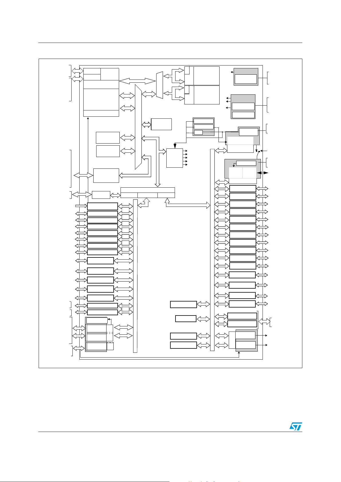
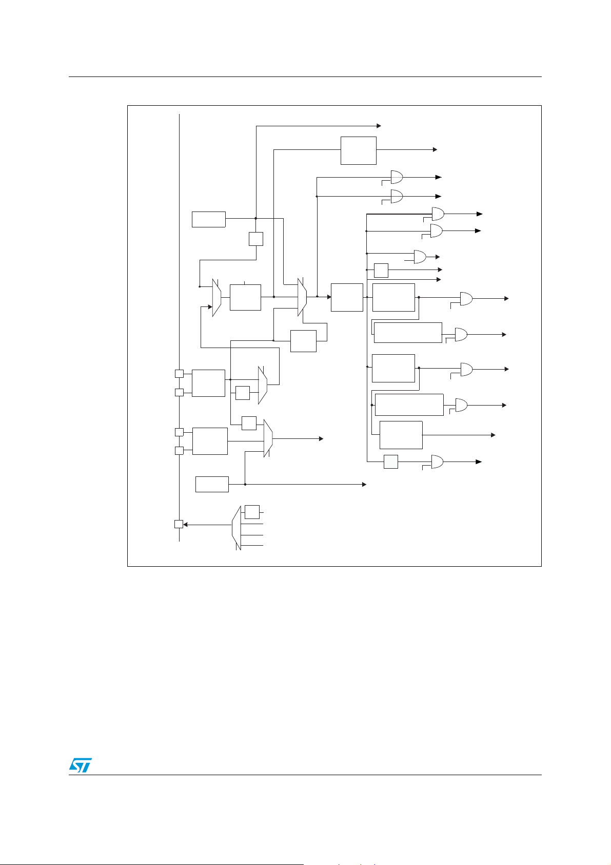
2.1 Device overview
The STM32F103xx XL-density performance line family offers devices in four different
package types: from 64 pins to 144 pins. Depending on the device chosen, different sets of
peripherals are included, the description below gives an overview of the complete range of
peripherals proposed in this family.
Figure 1 shows the general block diagram of the device family.
Table 2. STM32F103xF and STM32F103xG features and peripheral counts
Peripherals STM32F103Rx STM32F103Vx STM32F103Zx
Flash memory 768 KB 1 MB 768 KB 1 MB 768 KB 1 MB
SRAM in Kbytes 96 96 96
FSMC No Yes
General-purpose 10
Timers
Advanced-control 2
Basic 2
SPI(I2S)
2
I
(2)
3(2)
C2
(1)
Ye s
Comm
USART 5
USB 1
CAN 1
SDIO 1
GPIOs 51 80 112
12-bit ADC
Number of channels
12-bit DAC
Number of channels
16
3
16
3
3
21
2
2
CPU frequency 72 MHz
Operating voltage 2.0 to 3.6 V
Operating temperatures
Ambient temperatures: –40 to +85 °C /–40 to +105 °C (see Ta b l e 1 0 )
Junction temperature: –40 to + 125 °C (see Table 10)
Package LQFP64 LQFP100 LQFP144, BGA144
1. For the LQFP100 package, only FSMC Bank1 and Bank2 are available. Bank1 can only support a
multiplexed NOR/PSRAM memory using the NE1 Chip Select. Bank2 can only support a 16- or 8-bit NAND
Flash memory using the NCE2 Chip Select. The interrupt line cannot be used since Port G is not available
in this package.
2. The SPI2 and SPI3 interfaces give the flexibility to work in an exclusive way in either the SPI mode or the
2
I
S audio mode.
Doc ID 16554 Rev 3 11/120
PA[ 15:0 ]
EXT.IT
WWDG
NVIC
12bit A DC1
8 ADINs common
JTDI
JTCK/SWCLK
JTMS/SWDA T
NJTRST
JTDO
=2 to 3.6V
112 AF
AHB2
MOSI/SD,MISO,
WKUP
F
max
: 48/72 MHz
V
SS
SCL,SDA,SMBA
I2C2
GP DMA1
XTAL OSC
4-16 MHz
XTAL 32 kHz
A
P
B
1:
F
m
a
x
=2
4
/
3
6MHz
HCLK
PCLK1
as AF
Flash1 512 KB
VOLT. RE G.
3.3VTO1.8V
POWER
Backupinterface
as AF
B
us matrix
64 bit
RTC
RC HS
Cortex-M3 CPU
Ibus
Dbus
obl
SRAM 512B
USART1
USART2
SPI2/I2S2
bxCAN device
7channels
Backup
reg
4channels
TIM1
4compl.
SCL,SDA,SMBA
I2C1
as AF
RX,TX, CTS,RTS,
USART3
Temp sen sor
4Ch,ETRas AF
FCLK
RC LS
Standby
IWDG
@VSW
POR / PD R
SUPPLY
@VDDA
V
BAT
=1.8Vto3.6V
CK as AF
RX,TX, CTS,RTS,
CK as AF
RX,TX, CTS,RTS,
CK as AF
A
PB
2:
F
m
a
x
=48 /
72
MH
z
NVIC
SPI1
MOSI,MISO,
SCK,NSS as AF
12bit A DC2
IF
IF
interface
SUPERVISION
PVD
Reset
Int
AWU
POR
TAMPER-RTC
System
SCK/CK ,NSS/WS,
UART4
RX,TX as AF
UART5
RX,TX as AF
Reset &
clock
controller
PCLK2
PLL
12bit DAC1
IFIF
IF
12bit DA C2
DAC1_OUT as AF
DAC2_OUT as AF
to the 3 ADCs
8 ADINs commo n
to the ADC1 & 2
GP DMA2
5channels
(ALARM OUT)
MCLK as AF
MOSI/SD,MISO,
SCK/CK ,NSS/WS,
MCLK as AF
SWJTAG
TPIU
ETM
Trace/Trig
TRACECL K
TRACED[ 0:3]
as AF
USBDM/CAN_RX
USBDP/CAN_TX
SDIO
FSMC
PCLK3
SRAM
96 Kbyte
64 bit
12bit ADC3
IF
5ADINs on ADC3
4
4compl.
BKIN, ETR input as AF
PB[15:0]
PC[ 15:0]
PD[15:0]
PE[1 5:0]
PF[15:0]
PG[15:0]
MPU
2 as AF
1 as AF
1 as AF
4Ch,ETRas AF
4Ch,ETRas AF
4Ch,ETRas AF
D[7: 0], CMD
CK as AF
Flash2 512 KB
A[25:0]
D[15:0]
CLK
NOE
NWE
NE[3:0]
NBL[1:0]
NWAIT
NL
as AF
channels
channels
channels
channels
channel
channel
TIM8
TIM9
TIM10
TIM11
V
REF+
V
REF–
TIM6
TIM7
TIM2
TIM3
TIM4
TIM5
TIM12
TIM13
TIM14
OSC_IN
OSC_OUT
OSC32_IN
OSC32_OUT
V
DD
@V
DD
NRST
V
DDA
V
SSA
V
DD
@V
DD
@V
DDA
@V
DDA
Flash
interface
Flash
interface
obl
2 channels as AF
1 channel as AF
1 channel as AF
ai17352
@V
DDA
GPIO port A
GPIO port B
GPIO port C
GPIO port D
GPIO port E
GPIO port F
GPIO port G
APB3 APB2 APB1
BKIN, ETR input as AF
USB 2.0 FS device
SPI3/I2S3
Description STM32F103xF, STM32F103xG
Figure 1. STM32F103xF and STM32F103xG performance line block diagram
1. TA = –40 °C to +85 °C (suffix 6, see Table 73) or –40 °C to +105 °C (suffix 7, see Table 73), junction temperature up to
2. AF = alternate function on I/O port pin.
105 °C or 125 °C, respectively.
12/120 Doc ID 16554 Rev 3
STM32F103xF, STM32F103xG Description
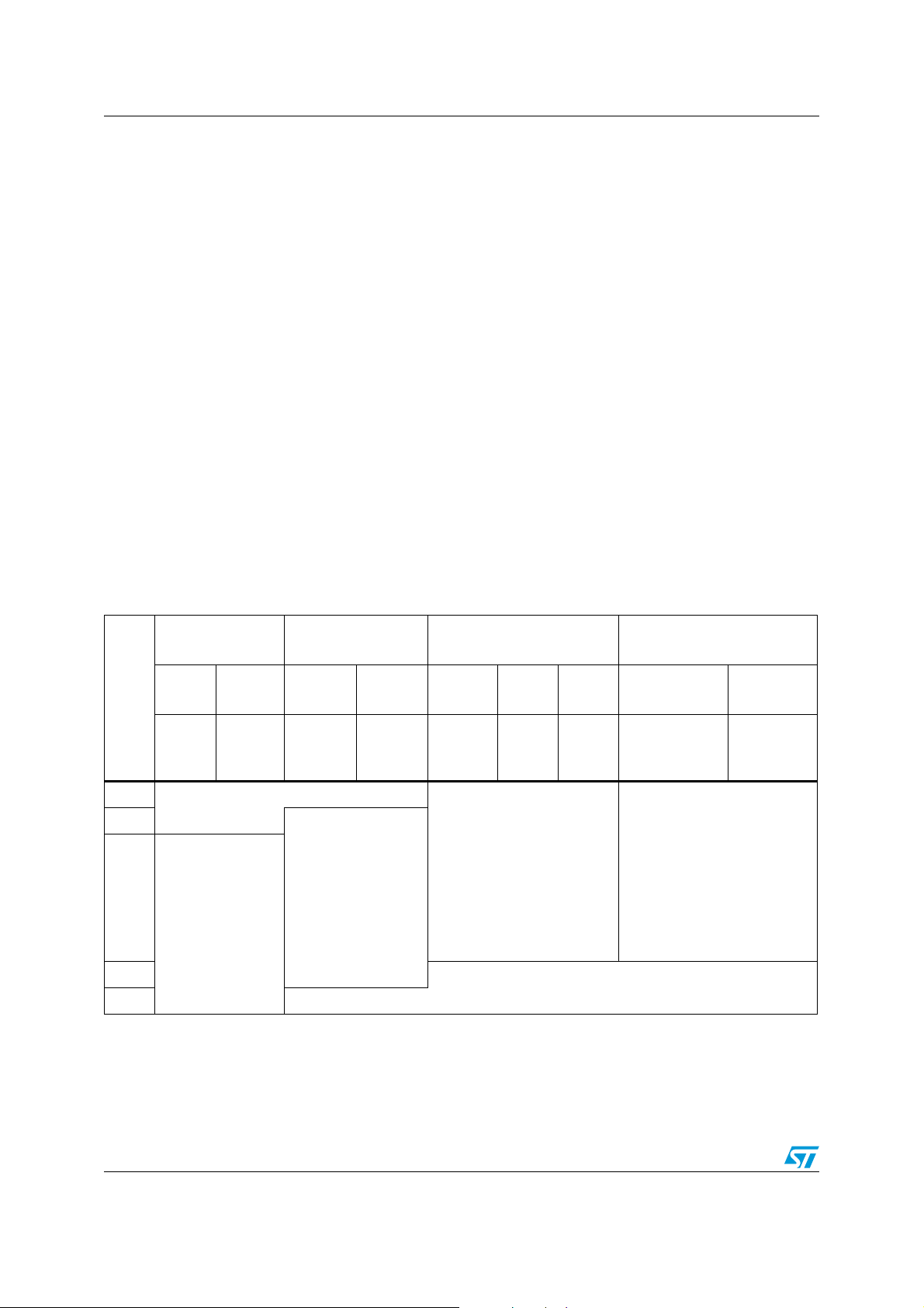
Figure 2. Clock tree
FLITFCLK
to Flash programming interface
USBCLK
to USB interface
I2S3CLK
I2S2CLK
36 MHz max
Peripheral Clock
Enable
else x2
72 MHz max
Peripheral Clock
Enable
else x2
ADCCLK
Peripheral clock
enable
to I2S3
to I2S2
SDIOCLK
FSMCCLK
HCLK
to AHB bus, core,
memory and DMA
to SDIO
to FSMC
to Cortex System timer
FCLK Cortex
free running clock
Peripheral Clock
Enable
PCLK1
to APB1
peripherals
to TIM2/3/4/5/12/13/14
and TIM6/7
TIMxCLK
PCLK2
peripherals to APB2
to TIM1/8
and TIM9/10/11
TIMxCLK
Peripheral Clock
Enable
to ADC1, 2 or 3
HCLK/2
To SDIO AHB interface
OSC_OUT
OSC_IN
OSC32_IN
OSC32_OUT
8 MHz
HSI RC
PLLSRC
4-16 MHz
HSE OSC
LSE OSC
32.768 kHz
LSI RC
40 kHz
HSI
PLLMUL
..., x16
x2, x3, x4
PLL
PLLXTPRE
/2
/128
LSE
RTCSEL[1:0]
LSI
/2
SW
HSI
PLLCLK
HSE
CSS
RTCCLK
to Independent Watchdog (IWDG)
SYSCLK
72 MHz
max
to RTC
AHB
Prescaler
/1, 2..512
IWDGCLK
USB
Prescaler
/1, 1.5
Peripheral clock
enable
Peripheral clock
enable
/1, 2, 4, 8, 16
TIM2,3,4,5,12,13,14,6,7
If (APB1 prescaler =1) x1
/1, 2, 4, 8, 16
48 MHz
Peripheral clock
enable
Peripheral clock
enable
72 MHz max
Clock
Enable
/8
APB1
Prescaler
APB2
Prescaler
TIM1, 8, 9, 10, 11
If (APB2 prescaler =1) x1
ADC
Prescaler
/2, 4, 6, 8
/2
Legend:
HSE = High-speed external clock signal
HSI =
High-speed internal clock signal
LSI =
Low-speed internal clock signal
LSE =
Low-speed external clock signal
ai17354
MCO
Main
Clock Output
/2
PLLCLK
HSI
HSE
SYSCLK
MCO
1. When the HSI is used as a PLL clock input, the maximum system clock frequency that can be achieved is
64 MHz.
2. For the USB function to be available, both HSE and PLL must be enabled, with the USBCLK at 48 MHz.
3. To have an ADC conversion time of 1 µs, APB2 must be at 14 MHz, 28 MHz or 56 MHz.
Doc ID 16554 Rev 3 13/120
Description STM32F103xF, STM32F103xG
2.2 Full compatibility throughout the family
The STM32F103xx is a complete family whose members are fully pin-to-pin, software and
feature compatible. In the reference manual, the STM32F103x4 and STM32F103x6 are
identified as low-density devices, the STM32F103x8 and STM32F103xB are referred to as
medium-density devices, the STM32F103xC, STM32F103xD and STM32F103xE are
referred to as high-density devices and the STM32F103xF and STM32F103xG are called
XL-density devices.
Low-density, high-density and XL-density devices are an extension of the STM32F103x8/B
medium-density devices, they are specified in the STM32F103x4/6, STM32F103xC/D/E and
STM32F103xF/G datasheets, respectively. Low-density devices feature lower Flash
memory and RAM capacities, less timers and peripherals. High-density devices have higher
Flash memory and RAM capacities, and additional peripherals like SDIO, FSMC, I
DAC. XL-density devices bring even more Flash and RAM memory, and extra features,
namely an MPU, a greater number of timers and a dual bank Flash structure while
remaining fully compatible with the other members of the family.
The STM32F103x4, STM32F103x6, STM32F103xC, STM32F103xD, STM32F103xE,
STM32F103xF and STM32F103xG are a drop-in replacement for the STM32F103x8/B
devices, allowing the user to try different memory densities and providing a greater degree
of freedom during the development cycle.
Moreover, the STM32F103xx performance line family is fully compatible with all existing
STM32F101xx access line and STM32F102xx USB access line devices.
Table 3. STM32F103xx family
2
S and
Pinout
144
100
64
48
Low-density
devices
16 KB
Flash
6 KB
RAM
32 KB
Flash
10 KB
RAM
2 × USARTs
2 × 16-bit timers
1 × SPI, 1 × I
2
C,
USB, CAN,
1 × PWM timer
2 × ADCs
Medium-density
devices
64 KB
(1)
Flash
20 KB
RAM
3 × USARTs
3 × 16-bit timers
2 × SPIs, 2 × I2Cs,
USB, CAN,
1 × PWM timer
2 × ADCs
128 KB
Flash
20 KB
RAM
High-density devices XL-density devices
256 KB
Flash
48 or
64 KB
RAM
5 × USARTs
4 × 16-bit timers,
2 × basic timers
3 × SPIs, 2 × I
USB, CAN, 2 × PWM timers
3 × ADCs, 2 × DACs,
1 × SDIO
FSMC (100- and 144-pin
packages
(2)
384 KB
Flash
64 KB
RAM
(3)
)
2
512 KB
Flash
64 KB
RAM
Ss, 2 × I2Cs
768 KB Flash 1 MB Flash
96 KB RAM 96 KB RAM
5 × USARTs
10 × 16-bit timers,
2 × basic timers
3 × SPIs, 2 × I
USB, CAN, 2 × PWM timers
3 × ADCs, 2 × DACs, 1 × SDIO,
Cortex-M3 with MPU
FSMC (100- and 144-pin
packages
(4)
), dual bank Flash
memory
36
1. For orderable part numbers that do not show the A internal code after the temperature range code (6 or 7), the reference
datasheet for electrical characteristics is that of the STM32F103x8/B medium-density devices.
2. 64 KB RAM for 256 KB Flash are available on devices delivered in CSP packages only.
3. Ports F and G are not available in devices delivered in 100-pin packages.
4. Ports F and G are not available in devices delivered in 100-pin packages.
2
Ss, 2 × I2Cs
14/120 Doc ID 16554 Rev 3

STM32F103xF, STM32F103xG Description
2.3 Overview
2.3.1 ARM® Cortex™-M3 core with embedded Flash and SRAM
The ARM Cortex™-M3 processor is the latest generation of ARM processors for embedded
systems. It has been developed to provide a low-cost platform that meets the needs of MCU
implementation, with a reduced pin count and low-power consumption, while delivering
outstanding computational performance and an advanced system response to interrupts.
The ARM Cortex™-M3 32-bit RISC processor features exceptional code-efficiency,
delivering the high-performance expected from an ARM core in the memory size usually
associated with 8- and 16-bit devices.
With its embedded ARM core, STM32F103xF and STM32F103xG performance line family
is compatible with all ARM tools and software.
Figure 1 shows the general block diagram of the device family.
2.3.2 Memory protection unit
The memory protection unit (MPU) is used to separate the processing of tasks from the data
protection. The MPU can manage up to 8 protection areas that can all be further divided up
into 8 subareas. The protection area sizes are between 32 bytes and the whole 4 gigabytes
of addressable memory.
The memory protection unit is especially helpful for applications where some critical or
certified code has to be protected against the misbehavior of other tasks. It is usually
managed by an RTOS (real-time operating system). If a program accesses a memory
location that is prohibited by the MPU, the RTOS can detect it and take action. In an RTOS
environment, the kernel can dynamically update the MPU area setting, based on the
process to be executed.
The MPU is optional and can be bypassed for applications that do not need it.
2.3.3 Embedded Flash memory
768 Kbytes to 1 Mbyte of embedded Flash are available for storing programs and data. The
Flash memory is organized as two banks. The first bank has a size of 512 Kbytes. The
second bank is either 256 or 512 Kbytes depending on the device. This gives the device the
capability of writing to one bank while executing code from the other bank (read-while-write
capability).
2.3.4 CRC (cyclic redundancy check) calculation unit
The CRC (cyclic redundancy check) calculation unit is used to get a CRC code from a 32-bit
data word and a fixed generator polynomial.
Among other applications, CRC-based techniques are used to verify data transmission or
storage integrity. In the scope of the EN/IEC 60335-1 standard, they offer a means of
verifying the Flash memory integrity. The CRC calculation unit helps compute a signature of
the software during runtime, to be compared with a reference signature generated at linktime and stored at a given memory location.
Doc ID 16554 Rev 3 15/120

Description STM32F103xF, STM32F103xG
2.3.5 Embedded SRAM
96 Kbytes of embedded SRAM accessed (read/write) at CPU clock speed with 0 wait states.
2.3.6 FSMC (flexible static memory controller)
The FSMC is embedded in the STM32F103xF and STM32F103xG performance line family.
It has four Chip Select outputs supporting the following modes: PC Card/Compact Flash,
SRAM, PSRAM, NOR and NAND.
Functionality overview:
● The three FSMC interrupt lines are ORed in order to be connected to the NVIC
● Write FIFO
● Code execution from external memory except for NAND Flash and PC Card
● The targeted frequency, f
, is HCLK/2, so external access is at 36 MHz when HCLK
CLK
is at 72 MHz and external access is at 24 MHz when HCLK is at 48 MHz
2.3.7 LCD parallel interface
The FSMC can be configured to interface seamlessly with most graphic LCD controllers. It
supports the Intel 8080 and Motorola 6800 modes, and is flexible enough to adapt to
specific LCD interfaces. This LCD parallel interface capability makes it easy to build costeffective graphic applications using LCD modules with embedded controllers or highperformance solutions using external controllers with dedicated acceleration.
2.3.8 Nested vectored interrupt controller (NVIC)
The STM32F103xF and STM32F103xG performance line embeds a nested vectored
interrupt controller able to handle up to 60 maskable interrupt channels (not including the 16
interrupt lines of Cortex™-M3) and 16 priority levels.
● Closely coupled NVIC gives low latency interrupt processing
● Interrupt entry vector table address passed directly to the core
● Closely coupled NVIC core interface
● Allows early processing of interrupts
● Processing of late arriving higher priority interrupts
● Support for tail-chaining
● Processor state automatically saved
● Interrupt entry restored on interrupt exit with no instruction overhead
This hardware block provides flexible interrupt management features with minimal interrupt
latency.
2.3.9 External interrupt/event controller (EXTI)
The external interrupt/event controller consists of 19 edge detector lines used to generate
interrupt/event requests. Each line can be independently configured to select the trigger
event (rising edge, falling edge, both) and can be masked independently. A pending register
maintains the status of the interrupt requests. The EXTI can detect an external line with a
pulse width shorter than the Internal APB2 clock period. Up to 112 GPIOs can be connected
to the 16 external interrupt lines.
16/120 Doc ID 16554 Rev 3

STM32F103xF, STM32F103xG Description
2.3.10 Clocks and startup
System clock selection is performed on startup, however the internal RC 8 MHz oscillator is
selected as default CPU clock on reset. An external 4-16 MHz clock can be selected, in
which case it is monitored for failure. If failure is detected, the system automatically switches
back to the internal RC oscillator. A software interrupt is generated if enabled. Similarly, full
interrupt management of the PLL clock entry is available when necessary (for example with
failure of an indirectly used external oscillator).
Several prescalers allow the configuration of the AHB frequency, the high speed APB
(APB2) and the low speed APB (APB1) domains. The maximum frequency of the AHB and
the high speed APB domains is 72 MHz. The maximum allowed frequency of the low speed
APB domain is 36 MHz. See
Figure 2 for details on the clock tree.
2.3.11 Boot modes
At startup, boot pins are used to select one of three boot options:
● Boot from user Flash: you have an option to boot from any of two memory banks. By
default, boot from Flash memory bank 1 is selected. You can choose to boot from Flash
memory bank 2 by setting a bit in the option bytes.
● Boot from system memory
● Boot from embedded SRAM
The boot loader is located in system memory. It is used to reprogram the Flash memory by
using USART1.
2.3.12 Power supply schemes
● V
● V
● V
For more details on how to connect power pins, refer to Figure 10: Power supply scheme.
= 2.0 to 3.6 V: external power supply for I/Os and the internal regulator.
DD
Provided externally through V
, V
SSA
= 2.0 to 3.6 V: external analog power supplies for ADC, DAC, Reset blocks,
DDA
RCs and PLL (minimum voltage to be applied to VDDA is 2.4 V when the ADC or DAC
is used). V
= 1.8 to 3.6 V: power supply for RTC, external clock 32 kHz oscillator and backup
BAT
DDA
and V
registers (through power switch) when V
2.3.13 Power supply supervisor
The device has an integrated power-on reset (POR)/power-down reset (PDR) circuitry. It is
always active, and ensures proper operation starting from/down to 2 V. The device remains
in reset mode when V
external reset circuit.
The device features an embedded programmable voltage detector (PVD) that monitors the
V
DD/VDDA
generated when V
than the V
message and/or put the MCU into a safe state. The PVD is enabled by software. Refer to
Ta bl e 12: Embedded reset and power control block characteristics for the values of
V
POR/PDR
power supply and compares it to the V
DD/VDDA
threshold. The interrupt service routine can then generate a warning
PVD
and V
PVD
pins.
DD
must be connected to VDD and VSS, respectively.
SSA
DD
is below a specified threshold, V
DD
drops below the V
PVD
.
is not present.
POR/PDR
threshold. An interrupt can be
PVD
, without the need for an
threshold and/or when VDD/V
is higher
DDA
Doc ID 16554 Rev 3 17/120

Description STM32F103xF, STM32F103xG
2.3.14 Voltage regulator
The regulator has three operation modes: main (MR), low power (LPR) and power down.
● MR is used in the nominal regulation mode (Run)
● LPR is used in the Stop modes.
● Power down is used in Standby mode: the regulator output is in high impedance: the
kernel circuitry is powered down, inducing zero consumption (but the contents of the
registers and SRAM are lost)
This regulator is always enabled after reset. It is disabled in Standby mode.
2.3.15 Low-power modes
The STM32F103xF and STM32F103xG performance line supports three low-power modes
to achieve the best compromise between low power consumption, short startup time and
available wakeup sources:
● Sleep mode
In Sleep mode, only the CPU is stopped. All peripherals continue to operate and can
wake up the CPU when an interrupt/event occurs.
● Stop mode
Stop mode achieves the lowest power consumption while retaining the content of
SRAM and registers. All clocks in the 1.8 V domain are stopped, the PLL, the HSI RC
and the HSE crystal oscillators are disabled. The voltage regulator can also be put
either in normal or in low-power mode.
The device can be woken up from Stop mode by any of the EXTI line. The EXTI line
source can be one of the 16 external lines, the PVD output, the RTC alarm or the USB
wakeup.
● Standby mode
The Standby mode is used to achieve the lowest power consumption. The internal
voltage regulator is switched off so that the entire 1.8 V domain is powered off. The
PLL, the HSI RC and the HSE crystal oscillators are also switched off. After entering
Standby mode, SRAM and register contents are lost except for registers in the Backup
domain and Standby circuitry.
The device exits Standby mode when an external reset (NRST pin), an IWDG reset, a
rising edge on the WKUP pin, or an RTC alarm occurs.
Note: The RTC, the IWDG, and the corresponding clock sources are not stopped by entering Stop
or Standby mode.
2.3.16 DMA
The flexible 12-channel general-purpose DMAs (7 channels for DMA1 and 5 channels for
DMA2) are able to manage memory-to-memory, peripheral-to-memory and memory-toperipheral transfers. The two DMA controllers support circular buffer management,
removing the need for user code intervention when the controller reaches the end of the
buffer.
18/120 Doc ID 16554 Rev 3
Each channel is connected to dedicated hardware DMA requests, with support for software
trigger on each channel. Configuration is made by software and transfer sizes between
source and destination are independent.
STM32F103xF, STM32F103xG Description
The DMA can be used with the main peripherals: SPI, I2C, USART, general-purpose, basic
and advanced-control timers TIMx, DAC, I
2
S, SDIO and ADC.
2.3.17 RTC (real-time clock) and backup registers
The RTC and the backup registers are supplied through a switch that takes power either on
V
supply when present or through the V
DD
pin. The backup registers are forty-two 16-bit
BAT
registers used to store 84 bytes of user application data when V
They are not reset by a system or power reset, and they are not reset when the device
wakes up from the Standby mode.
The real-time clock provides a set of continuously running counters which can be used with
suitable software to provide a clock calendar function, and provides an alarm interrupt and a
periodic interrupt. It is clocked by a 32.768 kHz external crystal, resonator or oscillator, the
internal low power RC oscillator or the high-speed external clock divided by 128. The
internal low-speed RC has a typical frequency of 40 kHz. The RTC can be calibrated using
an external 512 Hz output to compensate for any natural quartz deviation. The RTC features
a 32-bit programmable counter for long term measurement using the Compare register to
generate an alarm. A 20-bit prescaler is used for the time base clock and is by default
configured to generate a time base of 1 second from a clock at 32.768 kHz.
2.3.18 Timers and watchdogs
The XL-density STM32F103xx performance line devices include up to two advanced-control
timers, up to ten general-purpose timers, two basic timers, two watchdog timers and a
SysTick timer.
power is not present.
DD
Ta bl e 4 compares the features of the advanced-control, general-purpose and basic timers.
Table 4. STM32F103xF and STM32F103xG timer feature comparison
Timer
TIM1, TIM8 16-bit
TIM2, TIM3,
TIM4, TIM5
TIM9, TIM12 16-bit Up
TIM10, TIM11
TIM13, TIM14
TIM6, TIM7 16-bit Up
Counter
resolution
16-bit
16-bit Up
Counter
type
Up,
down,
up/down
Up,
down,
up/down
Prescaler factor
Any integer between
1 and 65536
Any integer between
1 and 65536
Any integer between
1 and 65536
Any integer between
1 and 65536
Any integer between
1 and 65536
DMA request
generation
Ye s 4 Ye s
Ye s 4 N o
No 2 No
No 1 No
Ye s 0 N o
Capture/compare
channels
Complementary
outputs
Doc ID 16554 Rev 3 19/120

Description STM32F103xF, STM32F103xG
Advanced-control timers (TIM1 and TIM8)
The two advanced-control timers (TIM1 and TIM8) can each be seen as a three-phase
PWM multiplexed on 6 channels. They have complementary PWM outputs with
programmable inserted dead-times. They can also be seen as a complete general-purpose
timer. The 4 independent channels can be used for:
● Input capture
● Output compare
● PWM generation (edge or center-aligned modes)
● One-pulse mode output
If configured as a standard 16-bit timer, it has the same features as the TIMx timer. If
configured as the 16-bit PWM generator, it has full modulation capability (0-100%).
In debug mode, the advanced-control timer counter can be frozen and the PWM outputs
disabled to turn off any power switch driven by these outputs.
Many features are shared with those of the general-purpose TIM timers which have the
same architecture. The advanced-control timer can therefore work together with the TIM
timers via the Timer Link feature for synchronization or event chaining.
General-purpose timers (TIMx)
There are10 synchronizable general-purpose timers embedded in the STM32F103xF and
STM32F103xG performance line devices (see
● TIM2, TIM3, TIM4, TIM5
Ta bl e 4 for differences).
There are up to 4 synchronizable general-purpose timers (TIM2, TIM3, TIM4 and TIM5)
embedded in the STM32F103xF and STM32F103xG access line devices.
These timers are based on a 16-bit auto-reload up/down counter, a 16-bit prescaler
and feature 4 independent channels each for input capture/output compare, PWM or
one-pulse mode output. This gives up to 16 input captures / output compares / PWMs
on the largest packages.
Their counter can be frozen in debug mode. Any of the general-purpose timers can be
used to generate PWM outputs. They all have independent DMA request generation.
These timers are capable of handling quadrature (incremental) encoder signals and the
digital outputs from 1 to 3 hall-effect sensors.
● TIM10, TIM11 and TIM9
These timers are based on a 16-bit auto-reload upcounter and a 16-bit prescaler.
TIM10 and TIM11 feature one independent channel, whereas TIM9 has two
independent channels for input capture/output compare, PWM or one-pulse mode
output. They can be synchronized with the TIM2, TIM3, TIM4, TIM5 full-featured
general-purpose timers. They can also be used as simple time bases.
● TIM13, TIM14 and TIM12
These timers are based on a 16-bit auto-reload upcounter and a 16-bit prescaler.
TIM13 and TIM14 feature one independent channel, whereas TIM12 has two
independent channels for input capture/output compare, PWM or one-pulse mode
output. They can be synchronized with the TIM2, TIM3, TIM4, TIM5 full-featured
general-purpose timers. They can also be used as simple time bases.
20/120 Doc ID 16554 Rev 3

STM32F103xF, STM32F103xG Description
Basic timers TIM6 and TIM7
These timers are mainly used for DAC trigger generation. They can also be used as a
generic 16-bit time base.
Independent watchdog
The independent watchdog is based on a 12-bit downcounter and 8-bit prescaler. It is
clocked from an independent 40 kHz internal RC and as it operates independently from the
main clock, it can operate in Stop and Standby modes. It can be used either as a watchdog
to reset the device when a problem occurs, or as a free running timer for application timeout
management. It is hardware or software configurable through the option bytes. The counter
can be frozen in debug mode.
Window watchdog
The window watchdog is based on a 7-bit downcounter that can be set as free running. It
can be used as a watchdog to reset the device when a problem occurs. It is clocked from the
main clock. It has an early warning interrupt capability and the counter can be frozen in
debug mode.
SysTick timer
This timer is dedicated to real-time operating systems, but could also be used as a standard
down counter. It features:
● A 24-bit down counter
● Autoreload capability
● Maskable system interrupt generation when the counter reaches 0.
● Programmable clock source
2.3.19 I²C bus
Up to two I²C bus interfaces can operate in multimaster and slave modes. They can support
standard and fast modes.
They support 7/10-bit addressing mode and 7-bit dual addressing mode (as slave). A
hardware CRC generation/verification is embedded.
They can be served by DMA and they support SMBus 2.0/PMBus.
2.3.20 Universal synchronous/asynchronous receiver transmitters (USARTs)
The STM32F103xF and STM32F103xG performance line embeds three universal
synchronous/asynchronous receiver transmitters (USART1, USART2 and USART3) and
two universal asynchronous receiver transmitters (UART4 and UART5).
These five interfaces provide asynchronous communication, IrDA SIR ENDEC support,
multiprocessor communication mode, single-wire half-duplex communication mode and
have LIN Master/Slave capability.
The USART1 interface is able to communicate at speeds of up to 4.5 Mbit/s. The other
available interfaces communicate at up to 2.25 Mbit/s.
USART1, USART2 and USART3 also provide hardware management of the CTS and RTS
signals, Smart Card mode (ISO 7816 compliant) and SPI-like communication capability. All
interfaces can be served by the DMA controller except for UART5.
Doc ID 16554 Rev 3 21/120

Description STM32F103xF, STM32F103xG
2.3.21 Serial peripheral interface (SPI)
Up to three SPIs are able to communicate up to 18 Mbits/s in slave and master modes in
full-duplex and simplex communication modes. The 3-bit prescaler gives 8 master mode
frequencies and the frame is configurable to 8 bits or 16 bits. The hardware CRC
generation/verification supports basic SD Card/MMC modes.
All SPIs can be served by the DMA controller.
2.3.22 Inter-integrated sound (I2S)
Two standard I2S interfaces (multiplexed with SPI2 and SPI3) are available, that can be
operated in master or slave mode. These interfaces can be configured to operate with 16/32
bit resolution, as input or output channels. Audio sampling frequencies from 8 kHz up to
48
kHz are supported. When either or both of the I2S interfaces is/are configured in master
mode, the master clock can be output to the external DAC/CODEC at 256 times the
sampling frequency.
2.3.23 SDIO
An SD/SDIO/MMC host interface is available, that supports MultiMediaCard System
Specification Version 4.2 in three different databus modes: 1-bit (default), 4-bit and 8-bit.
The interface allows data transfer at up to 48 MHz in 8-bit mode, and is compliant with SD
Memory Card Specifications Version 2.0.
The SDIO Card Specification Version 2.0 is also supported with two different databus
modes: 1-bit (default) and 4-bit.
The current version supports only one SD/SDIO/MMC4.2 card at any one time and a stack
of MMC4.1 or previous.
In addition to SD/SDIO/MMC, this interface is also fully compliant with the CE-ATA digital
protocol Rev1.1.
2.3.24 Controller area network (CAN)
The CAN is compliant with specifications 2.0A and B (active) with a bit rate up to 1 Mbit/s. It
can receive and transmit standard frames with 11-bit identifiers as well as extended frames
with 29-bit identifiers. It has three transmit mailboxes, two receive FIFOs with 3 stages and
14 scalable filter banks.
2.3.25 Universal serial bus (USB)
The STM32F103xF and STM32F103xG performance line embed a USB device peripheral
compatible with the USB full-speed 12 Mbs. The USB interface implements a full-speed (12
Mbit/s) function interface. It has software-configurable endpoint setting and suspend/resume
support. The dedicated 48 MHz clock is generated from the internal main PLL (the clock
source must use a HSE crystal oscillator).
2.3.26 GPIOs (general-purpose inputs/outputs)
Each of the GPIO pins can be configured by software as output (push-pull or open-drain), as
input (with or without pull-up or pull-down) or as peripheral alternate function. Most of the
GPIO pins are shared with digital or analog alternate functions. All GPIOs are high currentcapable.
22/120 Doc ID 16554 Rev 3

STM32F103xF, STM32F103xG Description
The I/Os alternate function configuration can be locked if needed following a specific
sequence in order to avoid spurious writing to the I/Os registers.
2.3.27 ADC (analog to digital converter)
Three 12-bit analog-to-digital converters are embedded into STM32F103xF and
STM32F103xG performance line devices and each ADC shares up to 21 external channels,
performing conversions in single-shot or scan modes. In scan mode, automatic conversion
is performed on a selected group of analog inputs.
Additional logic functions embedded in the ADC interface allow:
● Simultaneous sample and hold
● Interleaved sample and hold
● Single shunt
The ADC can be served by the DMA controller.
An analog watchdog feature allows very precise monitoring of the converted voltage of one,
some or all selected channels. An interrupt is generated when the converted voltage is
outside the programmed thresholds.
The events generated by the general-purpose timers (TIMx) and the advanced-control
timers (TIM1 and TIM8) can be internally connected to the ADC start trigger and injection
trigger, respectively, to allow the application to synchronize A/D conversion and timers.
2.3.28 DAC (digital-to-analog converter)
The two 12-bit buffered DAC channels can be used to convert two digital signals into two
analog voltage signal outputs. The chosen design structure is composed of integrated
resistor strings and an amplifier in inverting configuration.
This dual digital Interface supports the following features:
● two DAC converters: one for each output channel
● 8-bit or 12-bit monotonic output
● left or right data alignment in 12-bit mode
● synchronized update capability
● noise-wave generation
● triangular-wave generation
● dual DAC channel independent or simultaneous conversions
● DMA capability for each channel
● external triggers for conversion
● input voltage reference V
Eight DAC trigger inputs are used in the STM32F103xF and STM32F103xG performance
line family. The DAC channels are triggered through the timer update outputs that are also
connected to different DMA channels.
REF+
Doc ID 16554 Rev 3 23/120

Description STM32F103xF, STM32F103xG
2.3.29 Temperature sensor
The temperature sensor has to generate a voltage that varies linearly with temperature. The
conversion range is between 2 V < V
< 3.6 V. The temperature sensor is internally
DDA
connected to the ADC1_IN16 input channel which is used to convert the sensor output
voltage into a digital value.
2.3.30 Serial wire JTAG debug port (SWJ-DP)
The ARM SWJ-DP Interface is embedded, and is a combined JTAG and serial wire debug
port that enables either a serial wire debug or a JTAG probe to be connected to the target.
The JTAG TMS and TCK pins are shared respectively with SWDIO and SWCLK and a
specific sequence on the TMS pin is used to switch between JTAG-DP and SW-DP.
2.3.31 Embedded Trace Macrocell™
The ARM® Embedded Trace Macrocell provides a greater visibility of the instruction and
data flow inside the CPU core by streaming compressed data at a very high rate from the
STM32F10xxx through a small number of ETM pins to an external hardware trace port
analyzer (TPA) device. The TPA is connected to a host computer using USB, Ethernet, or
any other high-speed channel. Real-time instruction and data flow activity can be recorded
and then formatted for display on the host computer running debugger software. TPA
hardware is commercially available from common development tool vendors. It operates
with third party debugger software tools.
24/120 Doc ID 16554 Rev 3
STM32F103xF, STM32F103xG Pinouts and pin descriptions
AI14798b
V
DD_7
PC3PC2
PF6
V
DD_6
V
SS_4
PF8
H
V
DD_1
D PG13
PG14
PE6PE5
C
PG10
PG11
V
DD_5
PB8
NRST
B PG12PG15
PC15-
OSC32_OUT
PB9
A
87654321
V
BAT
OSC_IN
OSC_OUT
V
SS_5
G
F
E
PF7
PC0
PF0 PF1
PF2
V
SS_10
PG9PF4
PF3
V
SS_3
PF5
V
DD_8
V
DD_3
V
DD_4
V
SS_8
PE4
PB5
PB6
BOOT0 PB7
V
SS_11
PF10
PC1
V
DD_11VDD_10
PF9
109
K
J
V
SS_2
PD3
PD4
PD1
PC12
PC11
PD5
PD2 PD0
V
DD_9
V
SS_9
V
DD_2
PG1
PC5PA5 PE9
PB2/
BOOT1
PC4PA4
PE10
PG0PF13V
REF–
PE12V
SSA
PA1 PE13
PA0-WKUP
PD9
PD10
PG4
PD13
1211
PG8
PA10
NC
PA9
PA11
PA12
PC10
PC9 PA8
PC7
PC6
PC8
PD14
PG3
PG2
PD15
M
L
PF15
PB1PA7 PE7
PF12
PB0PA6
PE8
PF14PF11V
DDA
PE14V
REF+
PA3 PE15
PA2
PB10
PD8
PD12
PB11
PB12
PB14
PB15
PB13
PC13-
TAMPER-RTC
PE3 PE2 PE1 PE0
PB4
JTRST
PB3
JTDO
PD6 PD7
PA15
JTDI
PA14
JTCK
PA13
JTMS
PE11V
SS_6
V
SS_7VSS_1
PG7
PD11
PG5
PG6
PC14-
OSC32_IN
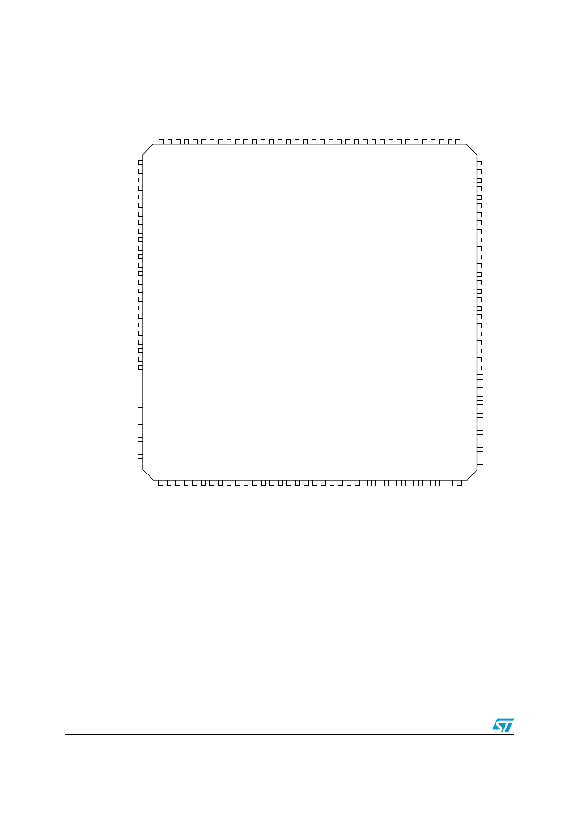
3 Pinouts and pin descriptions
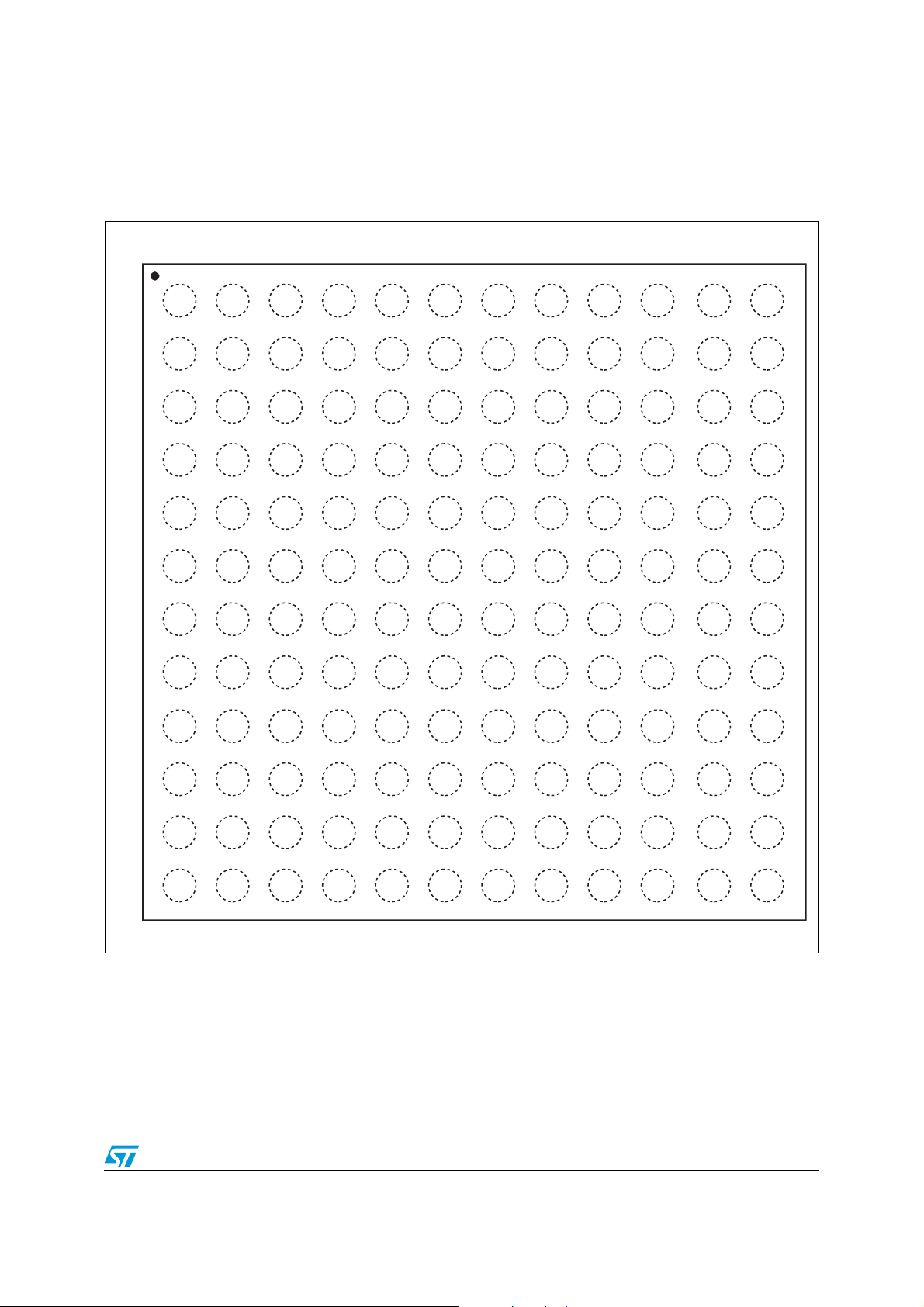
Figure 3. STM32F103xF and STM32F103xG XL-density performance line BGA144 ballout
Doc ID 16554 Rev 3 25/120
Pinouts and pin descriptions STM32F103xF, STM32F103xG
V
DD_3VSS_3
PE1
PE0
PB9
PB8
BOOT0
PB7
PB6
PB5
PB4
PB3
PG15
V
DD_11VSS_11
PG14
PG13
PG12
PG11
PG10
PG9
PD7
PD6
V
DD_10VSS_10
PD5
PD4
PD3
PD2
PD1
PD0
PC12
PC11
PC10
PA15
PA14
PE2
V
DD_2
PE3
V
SS_2
PE4
NC
PE5
PA13
PE6
PA12
VBAT
PA11
PC13-TAMPER-RTC
PA10
PC14-OSC32_IN
PA9
PC15-OSC32_OUT
PA8
PF0
PC9
PF1
PC8
PF2
PC7
PF3
PC6
PF4
V
DD_9
PF5
V
SS_9
V
SS_5
PG8
V
DD_5
PG7
PF6
PG6
PF7
PG5
PF8
PG4
PF9
PG3
PF10
PG2
OSC_IN
PD15
OSC_OUT
PD14
NRST
V
DD_8
PC0
V
SS_8
PC1
PD13
PC2
PD12
PC3
PD11
V
SSA
PD10
V
REF-
PD9
V
REF+
PD8
V
DDA
PB15
PA0-WKUP
PB14
PA1
PB13
PA2
PB12
PA3
V
SS_4
V
DD_4
PA4
PA5
PA6
PA7
PC4
PC5
PB0
PB1
PB2
PF11
PF12
VSS_6
V
DD_6
PF13
PF14
PF15
PG0
PG1
PE7
PE8
PE9
V
SS_7
V
DD_7
PE10
PE11
PE12
PE13
PE14
PE15
PB10
PB11
V
SS_1
V
DD_1
144
143
142
141
140
139
138
137
136
135
134
133
132
131
130
129
128
127
126
125
124
123
122
121
109
1
2
3
4
5
6
7
8
9
10
11
12
13
14
15
16
17
18
19
20
21
22
23
24
25
108
107
106
105
104
103
102
101
100
99
98
97
96
95
94
93
92
91
90
89
88
87
86
85
84
3738394041424344454647484950515253545556575859
60
72
LQFP144
120
119
118
117
116
115
114
113
112
111
110
6162636465666768697071
26
27
28
29
30
31
32
33
34
35
36
83
82
81
80
79
78
77
76
75
74
73
ai14667
Figure 4. STM32F103xF and STM32F103xG XL-density performance line LQFP144 pinout
26/120 Doc ID 16554 Rev 3
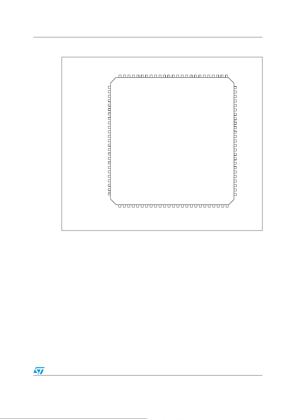
STM32F103xF, STM32F103xG Pinouts and pin descriptions
100999897969594939291908988878685848382818079787776
1
2
3
4
5
6
7
8
9
10
11
12
13
14
15
16
17
18
19
20
21
22
23
24
25
75
74
73
72
71
70
69
68
67
66
65
64
63
62
61
60
59
58
57
56
55
54
53
52
51
VDD_2
VSS_2
NC
PA 1 3
PA 1 2
PA 1 1
PA 1 0
PA 9
PA 8
PC9
PC8
PC7
PC6
PD15
PD14
PD13
PD12
PD11
PD10
PD9
PD8
PB15
PB14
PB13
PB12
PA 3
VSS_4
VDD_4
PA 4
PA 5
PA 6
PA 7
PC4
PC5
PB0
PB1
PB2
PE7
PE8
PE9
PE10
PE11
PE12
PE13
PE14
PE15
PB10
PB11
VSS_1
VDD_1
VDD_3
VSS_3
PE1
PE0
PB9
PB8
BOOT0
PB7
PB6
PB5
PB4
PB3
PD7
PD6
PD5
PD4
PD3
PD2
PD1
PD0
PC12
PC11
PC10
PA15
PA14
26272829303132333435363738394041424344454647484950
PE2
PE3
PE4
PE5
PE6
VBAT
PC13-TAMPER-RTC
PC14-OSC32_IN
PC15-OSC32_OUT
VSS_5
VDD_5
OSC_IN
OSC_OUT
NRST
PC0
PC1
PC2
PC3
VSSA
VREF-
VREF+
VDDA
PA 0- W K UP
PA 1
PA 2
ai14391
LQFP100
Figure 5. STM32F103xF and STM32F103xG XL-density performance line LQFP100
pinout
Doc ID 16554 Rev 3 27/120
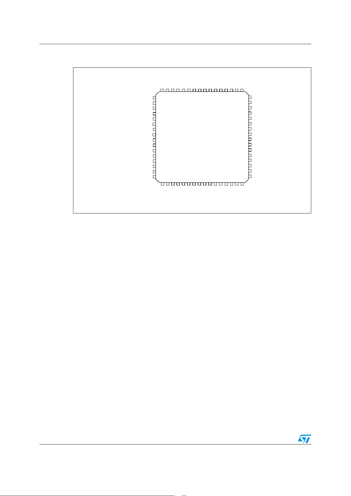
Pinouts and pin descriptions STM32F103xF, STM32F103xG
64 63 62 61 60 59 58 57 56 55 54 53 52 51 50 49
48
47
46
45
44
43
42
41
40
39
38
37
36
35
34
33
17 18 19 20 21 22 23 24 29 30 31 3225 26 27 28
1
2
3
4
5
6
7
8
9
10
11
12
13
14
15
16
VBAT
PC13-TAMPER-RTC
PC14-OSC32_IN
PC15-OSC32_OUT
PD0 OSC_IN
PD1 OSC_OUT
NRST
PC0
PC1
PC2
PC3
VSSA
VDDA
PA 0- W K UP
PA 1
PA 2
VDD_3
VSS_3
PB9
PB8
BOOT0
PB7
PB6
PB5
PB4
PB3
PD2
PC12
PC11
PC10
PA 1 5
PA 14
VDD_2
VSS_2
PA 1 3
PA 1 2
PA 1 1
PA 1 0
PA 9
PA 8
PC9
PC8
PC7
PC6
PB15
PB14
PB13
PB12
PA 3
VSS_4
VDD_4
PA 4
PA 5
PA 6
PA 7
PC4
PC5
PB0
PB1
PB2
PB10
PB11
VSS_1
VDD_1
LQFP64
ai14392
Figure 6. STM32F103xF and STM32F103xG XL-density performance line
LQFP64 pinout
28/120 Doc ID 16554 Rev 3
STM32F103xF, STM32F103xG Pinouts and pin descriptions
Pins
LQFP64
(2)
Pin name
(1)
Typ e
LQFP100
LQFP144
FT
FT
FT
FT
FT
BAT
PC13-TAMPER-
RTC
(5)
PC15-
OSC32_OUT
SV
I/O PC13
(5)
I/O PC14
I/O PC15
(5)
Main
function
(3)
(after reset)
I / O level
PE2 TRACECK / FSMC_A23
PE3 TRACED0 / FSMC_A19
PE4 TRACED1/ FSMC_A20
PE5 TRACED2/ FSMC_A21 TIM9_CH1
PE6 TRACED3 / FSMC_A22 TIM9_CH2
BAT
(6)
(6)
(6)
Alternate functions
Default Remap
TAMPER-RTC
OSC32_IN
OSC32_OUT
Table 5. STM32F103xF and STM32F103xG pin definitions
LFBGA144
A3 - 1 1 PE2 I/O
A2 - 2 2 PE3 I/O
B2 - 3 3 PE4 I/O
B3 - 4 4 PE5 I/O
B4 - 5 5 PE6 I/O
C2 1 6 6 V
A1 2 7 7
B1 3 8 8 PC14-OSC32_IN
C1 4 9 9
C3 - - 10 PF0 I/O FT PF0 FSMC_A0
C4 - - 11 PF1 I/O FT PF1 FSMC_A1
D4 - - 12 PF2 I/O FT PF2 FSMC_A2
E2 - - 13 PF3 I/O FT PF3 FSMC_A3
E3 - - 14 PF4 I/O FT PF4 FSMC_A4
E4 - - 15 PF5 I/O FT PF5 FSMC_A5
D2 - 10 16 V
D3 - 11 17 V
SS_5
DD_5
SV
SV
SS_5
DD_5
F3 - - 18 PF6 I/O PF6 ADC3_IN4 / FSMC_NIORD TIM10_CH1
F2 - - 19 PF7 I/O PF7 ADC3_IN5 / FSMC_NREG TIM11_CH1
G3 - - 20 PF8 I/O PF8 ADC3_IN6 / FSMC_NIOWR TIM13_CH1
G2 - - 21 PF9 I/O PF9 ADC3_IN7 / FSMC_CD TIM14_CH1
G1 - - 22 PF10 I/O PF10 ADC3_IN8 / FSMC_INTR
D1 5 12 23 OSC_IN I OSC_IN PD0
E1 6 13 24 OSC_OUT O OSC_OUT PD1
F1 7 14 25 NRST I/O NRST
H1 8 15 26 PC0 I/O PC0 ADC123_IN10
H2 9 16 27 PC1 I/O PC1 ADC123_IN11
H3 10 17 28 PC2 I/O PC2 ADC123_IN12
H4 11 18 29 PC3 I/O PC3 ADC123_IN13
J1 12 19 30 V
K1 - 20 31 V
SSA
REF-
SV
SV
SSA
REF-
(4)
(7)
(7)
Doc ID 16554 Rev 3 29/120
Pinouts and pin descriptions STM32F103xF, STM32F103xG
Table 5. STM32F103xF and STM32F103xG pin definitions (continued)
(7)
(7)
/
/
/
/
/
(4)
TIM1_BKIN
TIM1_CH1N
TIM1_CH2N
TIM1_CH3N
Pins
Pin name
LQFP64
LQFP100
LFBGA144
LQFP144
L1 - 21 32 V
M1 13 22 33 V
REF+
DDA
(2)
(1)
Type
Main
function
(3)
(after reset)
I / O level
SV
SV
REF+
DDA
WKUP/USART2_CTS
J2 14 23 34 PA0-WKUP I/O PA0
ADC123_IN0 / TIM2_CH1_ETR /
TIM5_CH1 / TIM8_ETR
K2 15 24 35 PA1 I/O PA1
USART2_RTS
TIM5_CH2 / TIM2_CH2
USART2_TX
L2 16 25 36 PA2 I/O PA2
ADC123_IN2 / TIM9_CH1 /
USART2_RX
M2 17 26 37 PA3 I/O PA3
G4 18 27 38 V
F4 19 28 39 V
SS_4
DD_4
SV
SV
SS_4
DD_4
J3 20 29 40 PA4 I/O PA4
K3 21 30 41 PA5 I/O PA5
ADC123_IN3 / TIM2_CH4
SPI1_NSS
DAC_OUT1 / ADC12_IN4
SPI1_SCK
SPI1_MISO
L3 22 31 42 PA6 I/O PA6
ADC12_IN6 / TIM3_CH1
SPI1_MOSI
M3 23 32 43 PA7 I/O PA7
ADC12_IN7 / TIM3_CH2
J4 24 33 44 PC4 I/O PC4 ADC12_IN14
K4 25 34 45 PC5 I/O PC5 ADC12_IN15
L4 26 35 46 PB0 I/O PB0
M4 27 36 47 PB1 I/O PB1
J5 28 37 48
PB2 I/O FT PB2/BOOT1
ADC12_IN8 / TIM3_CH3 /
ADC12_IN9 / TIM3_CH4
M5 - - 49 PF11 I/O FT PF11 FSMC_NIOS16
L5 - - 50 PF12 I/O FT PF12 FSMC_A6
H5 - - 51 V
G5 - - 52 V
SS_6
DD_6
SV
SV
SS_6
DD_6
K5 - - 53 PF13 I/O FT PF13 FSMC_A7
Alternate functions
Default Remap
(8)
/
(7)
/ ADC123_IN1 /
(7)
/ TIM5_CH3 /
TIM2_CH3
(7)
/ TIM5_CH4 /
(7)
(7)
TIM9_CH2
(7)
/ USART2_CK
(7)
/ DAC_OUT2 /
ADC12_IN5
(7)
/ TIM8_BKIN /
(7)
TIM13_CH1
(7)
/ TIM8_CH1N /
(7)
TIM14_CH1
TIM8_CH2N
(7)
TIM8_CH3N
30/120 Doc ID 16554 Rev 3

STM32F103xF, STM32F103xG Pinouts and pin descriptions
Table 5. STM32F103xF and STM32F103xG pin definitions (continued)
(7)
(7)
(7)
/
(4)
TIM2_CH3
TIM2_CH4
TIM4_CH1 /
USART3_RTS
Alternate functions
Default Remap
LFBGA144
Pins
LQFP64
(2)
Pin name
(1)
Type
LQFP100
LQFP144
Main
function
(after reset)
I / O level
(3)
M6 - - 54 PF14 I/O FT PF14 FSMC_A8
L6 - - 55 PF15 I/O FT PF15 FSMC_A9
K6 - - 56 PG0 I/O FT PG0 FSMC_A10
J6 - - 57 PG1 I/O FT PG1 FSMC_A11
M7 - 38 58 PE7 I/O FT PE7 FSMC_D4 TIM1_ETR
L7 - 39 59 PE8 I/O FT PE8 FSMC_D5 TIM1_CH1N
K7 - 40 60 PE9 I/O FT PE9 FSMC_D6 TIM1_CH1
H6 - - 61 V
G6 - - 62 V
SS_7
DD_7
SV
SV
SS_7
DD_7
J7 - 41 63 PE10 I/O FT PE10 FSMC_D7 TIM1_CH2N
H8 - 42 64 PE11 I/O FT PE11 FSMC_D8 TIM1_CH2
J8 - 43 65 PE12 I/O FT PE12 FSMC_D9 TIM1_CH3N
K8 - 44 66 PE13 I/O FT PE13 FSMC_D10 TIM1_CH3
L8 - 45 67 PE14 I/O FT PE14 FSMC_D11 TIM1_CH4
M8 - 46 68 PE15 I/O FT PE15 FSMC_D12 TIM1_BKIN
M9 29 47 69 PB10 I/O FT PB10 I2C2_SCL / USART3_TX
M10 30 48 70 PB11 I/O FT PB11 I2C2_SDA / USART3_RX
H7 31 49 71 V
G7 32 50 72 V
SS_1
DD_1
SV
SV
SS_1
DD_1
SPI2_NSS / I2S2_WS /
M11 33 51 73 PB12 I/O FT PB12
M12 34 52 74 PB13 I/O FT PB13
L11 35 53 75 PB14 I/O FT PB14
L12 36 54 76 PB15 I/O FT PB15
I2C2_SMBA / USART3_CK
TIM1_BKIN
SPI2_SCK / I2S2_CK /
USART3_CTS
SPI2_MISO / TIM1_CH2N /
USART3_RTS
SPI2_MOSI / I2S2_SD /
TIM1_CH3N
(7)
(7)
/ TIM1_CH1N
(7)
/ TIM12_CH1
(7)
/ TIM12_CH2
L9 - 55 77 PD8 I/O FT PD8 FSMC_D13 USART3_TX
K9 - 56 78 PD9 I/O FT PD9 FSMC_D14 USART3_RX
J9 - 57 79 PD10 I/O FT PD10 FSMC_D15 USART3_CK
H9 - 58 80 PD11 I/O FT PD11 FSMC_A16 USART3_CTS
L10 - 59 81 PD12 I/O FT PD12 FSMC_A17
Doc ID 16554 Rev 3 31/120

Pinouts and pin descriptions STM32F103xF, STM32F103xG
Table 5. STM32F103xF and STM32F103xG pin definitions (continued)
Alternate functions
Default Remap
LFBGA144
Pins
LQFP64
(2)
Pin name
(1)
Type
LQFP100
LQFP144
Main
function
(after reset)
I / O level
(3)
K10 - 60 82 PD13 I/O FT PD13 FSMC_A18 TIM4_CH2
G8 - - 83 V
F8 - - 84 V
SS_8
DD_8
SV
SV
SS_8
DD_8
K11 - 61 85 PD14 I/O FT PD14 FSMC_D0 TIM4_CH3
K12 - 62 86 PD15 I/O FT PD15 FSMC_D1 TIM4_CH4
J12 - - 87 PG2 I/O FT PG2 FSMC_A12
J11 - - 88 PG3 I/O FT PG3 FSMC_A13
J10 - - 89 PG4 I/O FT PG4 FSMC_A14
H12 - - 90 PG5 I/O FT PG5 FSMC_A15
H11 - - 91 PG6 I/O FT PG6 FSMC_INT2
H10 - - 92 PG7 I/O FT PG7 FSMC_INT3
G11 - - 93 PG8 I/O FT PG8
G10 - - 94 V
F10 - - 95 V
SS_9
DD_9
G12 37 63 96 PC6 I/O FT PC6
F12 38 64 97 PC7 I/O FT PC7
SV
SV
SS_9
DD_9
I2S2_MCK / TIM8_CH1 /
SDIO_D6
I2S3_MCK / TIM8_CH2 /
SDIO_D7
F11 39 65 98 PC8 I/O FT PC8 TIM8_CH3 / SDIO_D0 TIM3_CH3
E11 40 66 99 PC9 I/O FT PC9 TIM8_CH4 / SDIO_D1 TIM3_CH4
E 1 2 4 1 67 1 0 0 PA 8 I / O F T PA 8
USART1_CK / TIM1_CH1
D 1 2 4 2 6 8 1 0 1 PA 9 I / O F T PA 9 U SA R T1 _T X
D11 43 69 102 PA10 I/O FT PA10 USART1_RX
C12 44 70 103 PA11 I/O FT PA11
B12 45 71 104 PA12 I/O FT PA12
A12 46 72 105 PA13 I/O FT
JTMS-
SWDIO
USART1_CTS / USBDM /
CAN_RX
USART1_RTS / USBDP /
CAN_TX
MCO
(7)
/ TIM1_CH2
(7)
/ TIM1_CH3
(7)
/ TIM1_CH4
(7)
/ TIM1_ETR
(7)
(7)
(7)
C11 - 73 106 Not connected
G9 47 74 107
F9 48 75 108
A11 49 76 109
V
V
SS_2
DD_2
SV
SV
PA 1 4 I / O F T
SS_2
DD_2
JTCK-
SWCLK
(4)
TIM3_CH1
TIM3_CH2
/
(7)
(7)
PA 1 3
PA 1 4
32/120 Doc ID 16554 Rev 3

STM32F103xF, STM32F103xG Pinouts and pin descriptions
Table 5. STM32F103xF and STM32F103xG pin definitions (continued)
Pins
Pin name
LQFP64
LQFP100
LFBGA144
A10 50 77 110
B11 51 78 111
B10 52 79 112
C10 53 80 113
E10 - 81 114
D10 - 82 115
E9 54 83 116
D9 - 84 117
C9 - 85 118
B9 - 86 119
E7 - - 120
F7 - - 121
A8 - 87 122
A9 - 88 123
E8 - - 124
D8 - - 125
C8 - - 126
B8 - - 127
D7 - - 128
C7 - - 129
E6 - - 130 V
F6 - - 131 V
B7 - - 132
A7 55 89 133
A6 56 90 134
B6 57 91 135 PB5 I/O PB5
LQFP144
PA15 I/O FT JTDI SPI3_NSS / I2S3_WS
PC10 I/O FT PC10 UART4_TX / SDIO_D2
PC11 I/O FT PC11 UART4_RX / SDIO_D3
PC12 I/O FT PC12 UART5_TX / SDIO_CK
PD0 I/O FT PD0 FSMC_D2
PD1 I/O FT PD1 FSMC_D3
PD2 I/O FT PD2
PD3 I/O FT PD3 FSMC_CLK
PD4 I/O FT PD4 FSMC_NOE
PD5 I/O FT PD5 FSMC_NWE
V
SS_10
V
DD_10
PD6 I/O FT PD6 FSMC_NWAIT
PD7 I/O FT PD7 FSMC_NE1 / FSMC_NCE2
PG9 I/O FT PG9 FSMC_NE2 / FSMC_NCE3
PG10 I/O FT PG10 FSMC_NCE4_1 / FSMC_NE3
PG11 I/O FT PG11 FSMC_NCE4_2
PG12 I/O FT PG12 FSMC_NE4
PG13 I/O FT PG13 FSMC_A24
PG14 I/O FT PG14 FSMC_A25
SS_11
DD_11
PG15 I/O FT PG15
PB3/ I/O FT JTDO SPI3_SCK / I2S3_CK/
PB4 I/O FT NJTRST SPI3_MISO
(2)
(1)
Type
Main
function
(3)
(after reset)
I / O level
SV
SV
S
S
SS_10
DD_10
V
SS_11
V
DD_11
C6 58 92 136 PB6 I/O FT PB6 I2C1_SCL
D6 59 93 137 PB7 I/O FT PB7
Alternate functions
Default Remap
TIM3_ETR / UART5_RX /
SDIO_CMD
I2C1_SMBA / SPI3_MOSI /
I2S3_SD
(8)
/ TIM4_CH1
(8)
I2C1_SDA
/ FSMC_NADV /
TIM4_CH2
(9)
(9)
(8)
(8)
(4)
TIM2_CH1_ETR
PA15 /
USART3_TX
USART3_RX
USART3_CK
CAN_RX
CAN_TX
USART2_CTS
USART2_RTS
USART2_TX
USART2_RX
USART2_CK
PB3/TRACESWO
TIM2_CH2 /
SPI1_SCK
PB4 /
SPI1_MISO
TIM3_CH2 /
SPI1_MOSI
USART1_TX
USART1_RX
SPI1_NSS
TIM3_CH1
Doc ID 16554 Rev 3 33/120
Pinouts and pin descriptions STM32F103xF, STM32F103xG
Table 5. STM32F103xF and STM32F103xG pin definitions (continued)
Alternate functions
Default Remap
LFBGA144
Pins
LQFP64
(2)
Pin name
(1)
Type
LQFP100
LQFP144
Main
function
(after reset)
I / O level
(3)
D5 60 94 138 BOOT0 I BOOT0
C5 61 95 139 PB8 I/O FT PB8
B5 62 96 140 PB9 I/O FT PB9
TIM4_CH3
TIM4_CH4
(8)
/ SDIO_D4 /
TIM10_CH1
(8)
/ SDIO_D5 /
TIM11_CH1
A5 - 97 141 PE0 I/O FT PE0 TIM4_ETR / FSMC_NBL0
A4 - 98 142 PE1 I/O FT PE1 FSMC_NBL1
E5 63 99 143 V
F5 64 100 144 V
SS_3
DD_3
1. I = input, O = output, S = supply.
2. FT = 5 V tolerant.
3. Function availability depends on the chosen device.
4. If several peripherals share the same I/O pin, to avoid conflict between these alternate functions only one peripheral should
be enabled at a time through the peripheral clock enable bit (in the corresponding RCC peripheral clock enable register).
5. PC13, PC14 and PC15 are supplied through the power switch. Since the switch only sinks a limited amount of current (3
mA), the use of GPIOs PC13 to PC15 in output mode is limited: the speed should not exceed 2 MHz with a maximum load
of 30 pF and these IOs must not be used as a current source (e.g. to drive an LED).
6. Main function after the first backup domain power-up. Later on, it depends on the contents of the Backup registers even
after reset (because these registers are not reset by the main reset). For details on how to manage these IOs, refer to the
Battery backup domain and BKP register description sections in the STM32F10xxx reference manual, available from the
STMicroelectronics website: www.st.com.
7. For the LQFP64 package, the pins number 5 and 6 are configured as OSC_IN/OSC_OUT after reset, however the
functionality of PD0 and PD1 can be remapped by software on these pins. For the LQFP100 and LQFP144/BGA144
packages, PD0 and PD1 are available by default, so there is no need for remapping. For more details, refer to Alternate
function I/O and debug configuration section in the STM32F10xxx reference manual.
8. This alternate function can be remapped by software to some other port pins (if available on the used package). For more
details, refer to the Alternate function I/O and debug configuration section in the STM32F10xxx reference manual,
available from the STMicroelectronics website: www.st.com.
9. For devices delivered in LQFP64 packages, the FSMC function is not available.
SV
SV
SS_3
DD_3
(4)
I2C1_SCL/
CAN_RX
I2C1_SDA /
CAN_TX
34/120 Doc ID 16554 Rev 3

STM32F103xF, STM32F103xG Pinouts and pin descriptions
Table 6. FSMC pin definition
FSMC
Pins
CF CF/IDE
NOR/PSRAM/
SRAM
NOR/PSRAM Mux NAND 16 bit
LQFP100
PE2 A23 A23 Yes
PE3 A19 A19 Yes
PE4 A20 A20 Yes
PE5 A21 A21 Yes
PE6 A22 A22 Yes
PF0 A0 A0 A0 -
PF1 A1 A1 A1 -
PF2 A2 A2 A2 -
PF3 A3 A3 -
PF4 A4 A4 -
PF5 A5 A5 -
PF6 NIORD NIORD -
PF7 NREG NREG -
(1)
PF8 NIOWR NIOWR -
PF9 CD CD -
PF10 INTR INTR -
PF11 NIOS16 NIOS16 -
PF12 A6 A6 -
PF13 A7 A7 -
PF14 A8 A8 -
PF15 A9 A9 -
PG0 A10 A10 -
PG1 A11 -
PE7 D4 D4 D4 DA4 D4 Yes
PE8 D5 D5 D5 DA5 D5 Yes
PE9 D6 D6 D6 DA6 D6 Yes
PE10 D7 D7 D7 DA7 D7 Yes
PE11 D8 D8 D8 DA8 D8 Yes
PE12 D9 D9 D9 DA9 D9 Yes
PE13 D10 D10 D10 DA10 D10 Yes
PE14 D11 D11 D11 DA11 D11 Yes
PE15 D12 D12 D12 DA12 D12 Yes
PD8 D13 D13 D13 DA13 D13 Yes
Doc ID 16554 Rev 3 35/120

Pinouts and pin descriptions STM32F103xF, STM32F103xG
Table 6. FSMC pin definition (continued)
FSMC
Pins
CF CF/IDE
NOR/PSRAM/
SRAM
NOR/PSRAM Mux NAND 16 bit
LQFP100
PD9 D14 D14 D14 DA14 D14 Yes
PD10 D15 D15 D15 DA15 D15 Yes
PD11 A16 A16 CLE Yes
PD12 A17 A17 ALE Yes
PD13 A18 A18 Yes
PD14 D0 D0 D0 DA0 D0 Yes
PD15 D1 D1 D1 DA1 D1 Yes
PG2 A12 -
PG3 A13 -
PG4 A14 -
PG5 A15 -
PG6 INT2 -
PG7 INT3 -
PD0 D2 D2 D2 DA2 D2 Yes
(1)
PD1 D3 D3 D3 DA3 D3 Yes
PD3 CLK CLK Yes
PD4 NOE NOE NOE NOE NOE Yes
PD5 NWE NWE NWE NWE NWE Yes
PD6 NWAIT NWAIT NWAIT NWAIT NWAIT Yes
PD7 NE1 NE1 NCE2 Yes
PG9 NE2 NE2 NCE3 -
PG10 NCE4_1 NCE4_1 NE3 NE3 -
PG11 NCE4_2 NCE4_2 -
PG12 NE4 NE4 -
PG13 A24 A24 -
PG14 A25 A25 -
PB7 NADV NADV Yes
PE0 NBL0 NBL0 Yes
PE1 NBL1 NBL1 Yes
1. Ports F and G are not available in devices delivered in 100-pin packages.
36/120 Doc ID 16554 Rev 3

STM32F103xF, STM32F103xG Memory mapping
4 Memory mapping
The memory map is shown in Figure 7.
Figure 7. Memory map
Reserved 0xA000 1000 - 0xBFFF FFFF
FSMC register
FSMC bank4 PCCARD
FSMC bank3 NAND (NAND2)
FSMC bank2 NAND (NAND1)
FSMC bank1 NOR/PSRAM 4
FSMC bank1 NOR/PSRAM 3
FSMC bank1 NOR/PSRAM 2
FSMC bank1 NOR/PSRAM 1
Reserved
CRC
Reserved
Flash interfaces 1 & 2
Reserved
RCC
Reserved
DMA2
DMA1
Reserved
SDIO
Reserved
TIM11
TIM10
TIM9
Reserved
ADC3
USART1
TIM8
0xFFFF FFFF
0xE000 0000
0xDFFF FFFF
0xC000 0000
0xBFFF FFFF
0xA000 0000
0x9FFF FFFF
0x8000 0000
0x7FFF FFFF
0x6000 0000
0x5FFF FFFF
0x4000 0000
0x3FFF FFFF
0x2000 0000
0x1FFF FFFF
0x0000 0000
512-Mbyte
block 7
Cortex-M3's
internal
peripherals
512-Mbyte
block 6
Not used
512-Mbyte
block 5
FSMC register
512-Mbyte
block 4
FSMC bank 3
& bank4
512-Mbyte
block 3
FSMC bank1
& bank2
512-Mbyte
block 2
Peripherals
512-Mbyte
block 1
SRAM
512-Mbyte
block 0
Code
Reserved
SRAM (96 KB aliased
by bit-banding)
Option bytes
System memory
Reserved
Flash memory bank 2
(256 KB or 512 KB)
Flash memory bank 1
(512 KB)
Reserved
Aliased to Flash or system
memory depending on
BOOT pins
0x3FFF FFFF
0x2001 8000
0x2001 7FFF
0x2000 0000
0x1FFF F800 - 0x1FFF F80F
0x1FFF E000- 0x1FFF F7FF
0x0810 0000 - 0x1FFF DFFF
0x080F FFFF
0x0808 0000
0x0807 FFFF
0x0800 0000
0x0010 0000 - 0x07FF FFFF
0x000F FFFF
0x0000 0000
SPI1
TIM1
ADC2
ADC1
Port G
Port F
Port E
Port D
Port C
Port B
Port A
EXTI
AFIO
Reserved
DAC
PWR
BKP
Reserved
BxCAN
Shared USB/CAN SRAM 512
bytes
USB registers
I2C2
I2C1
UART5
UART4
USART3
USART2
Reserved
SPI3/I2S3
SPI2/I2S2
Reserved
IWDG
WWDG
RTC
Reserved
TIM14
TIM13
TIM12
TIM7
TIM6
TIM5
TIM4
TIM3
TIM2
0xA000 0000 - 0xA000 0FFF
0x9000 0000 - 0x9FFF FFFF
0x8000 0000 - 0x
0x7000 0000 - 0x7FFF FFFF
0x6C00 0000 - 0x6FFF FFFF
0x6800 0000 - 0x6BFF FFFF
0x6400 0000 - 0x67FF FFFF
0x6000 0000 - 0x63FF FFFF
0x4002 4400 - 0x5FFF FFFF
0x4002 3000 - 0x4002 33FF
0x4002 2400 - 0x4002 2FFF
0x4002 2000 - 0x4002 23FF
0x4002 1400 - 0x4002 1FFF
0x4002 1000 - 0x4002 13FF
0x4002 0400 - 0x4002 0FFF
0x4002 0400 - 0x4002 07FF
0x4002 0000 - 0x4002 03FF
0x4001 8400 - 0x4001 FFFF
0x4001 8000 - 0x4001 83FF
0x4001 5800 - 0x4001 7FFF
0x4001 5400 - 0x4001 57FF
0x4001 5000 - 0x4001 53FF
0x4001 4C00 - 0x4001 4FFF
0x4001 4000 - 0x4001 4BFF
0x4001 3C00 - 0x4001 3FFF
0x4001 3800 - 0x4001 3BFF
0x4001 3400 - 0x4001 37FF
0x4001 3000 - 0x4001 33FF
0x4001 2C00 - 0x4001 2FFF
0x4001 2800 - 0x4001 2BFF
0x4001 2400 - 0x4001 27FF
0x4001 2000 - 0x4001 23FF
0x4001 1C00 - 0x4001 1FFF
0x4001 1800 - 0x4001 1BFF
0x4001 1400 - 0x4001 17FF
0x4001 1000 - 0x4001 13FF
0x4001 0C00 - 0x4001 0FFF
0x4001 0800 - 0x4001 0BFF
0x4001 0400 - 0x4001 07FF
0x4001 0000 - 0x4001 03FF
0x4000 7800 - 0x4000 FFFF
0x4000 7400 - 0x4000 77FF
0x4000 7000 - 0x4000 73FF
0x4000 6C00 - 0x4000 6FFF
0x4000 6800 - 0x4000 6BFF
0x4000 6400 - 0x4000 67FF
0x4000 6000 - 0x4000 63FF
0x4000 5C00 - 0x4000 5FFF
0x4000 5800 - 0x4000 5BFF
0x4000 5400 - 0x4000 57FF
0x4000 5000 - 0x4000 53FF
0x4000 4C00 - 0x4000 4FFF
0x4000 4800 - 0x4000 4BFF
0x4000 4400 - 0x4000 47FF
0x4000 4000 - 0x4000 43FF
0x4000 3C00 - 0x4000 3FFF
0x4000 3800 - 0x4000 3BFF
0x4000 3400 - 0x4000 37FF
0x4000 3000 - 0x4000 33FF
0x4000 2C00 - 0x4000 2FFF
0x4000 2800 - 0x4000 2BFF
0x4000 2400 - 0x4000 27FF
0x4000 2000 - 0x4000 23FF
0x4000 1C00 - 0x4000 1FFF
0x4000 1800 - 0x4000 1BFF
0x4000 1400 - 0x4000 17FF
0x4000 1000 - 0x4000 13FF
0x4000 0C00 - 0x4000 0FFF
0x4000 0800 - 0x4000 0BFF
0x4000 0400 - 0x4000 07FF
0x4000 0000 - 0x4000 03FF
8FFF FFFF
ai17353
Doc ID 16554 Rev 3 37/120

Electrical characteristics STM32F103xF, STM32F103xG
ai14141
C = 50 pF
STM32F103xx pin
ai14142
STM32F103xx pin
V
IN
5 Electrical characteristics
5.1 Parameter conditions
Unless otherwise specified, all voltages are referenced to VSS.
5.1.1 Minimum and maximum values
Unless otherwise specified the minimum and maximum values are guaranteed in the worst
conditions of ambient temperature, supply voltage and frequencies by tests in production on
100% of the devices with an ambient temperature at T
the selected temperature range).
Data based on characterization results, design simulation and/or technology characteristics
are indicated in the table footnotes and are not tested in production. Based on
characterization, the minimum and maximum values refer to sample tests and represent the
mean value plus or minus three times the standard deviation (mean±3
5.1.2 Typical values
Unless otherwise specified, typical data are based on TA = 25 °C, VDD = 3.3 V (for the
2
V ≤ V
tested.
≤ 3.6 V voltage range). They are given only as design guidelines and are not
DD
= 25 °C and TA = TAmax (given by
A
Σ).
Typical ADC accuracy values are determined by characterization of a batch of samples from
a standard diffusion lot over the full temperature range, where 95% of the devices have an
error less than or equal to the value indicated
5.1.3 Typical curves
Unless otherwise specified, all typical curves are given only as design guidelines and are
not tested.
5.1.4 Loading capacitor
The loading conditions used for pin parameter measurement are shown in Figure 8.
5.1.5 Pin input voltage
The input voltage measurement on a pin of the device is described in Figure 9.
Figure 8. Pin loading conditions Figure 9. Pin input voltage
(mean±2Σ).
38/120 Doc ID 16554 Rev 3

STM32F103xF, STM32F103xG Electrical characteristics
ai14126
V
BAT
V
DD
V
DDA
IDD_V
BAT
I
DD
5.1.6 Power supply scheme
Figure 10. Power supply scheme
N&
&
6
§N&
§&
6
$$
N&
&
6
$$
6
6
2%&
6
'0)/ S
$$
6
33
6
6
2%&
6
6
"!4
$$!
2%&
33!
0OWERSWITCH
/54
).
2EGULATOR
!$#
$!#
"ACKUPCIRCUITRY
/3#+24#
7AKEUPLOGIC
"ACKUPREGISTERS
)/
,OGIC
,EVELSHIFTER
!NALO G
2#S0,,
+ERNELLOGIC
#05
$IGITAL
-EMORIES
AI
Caution: In Figure 10, the 4.7 µF capacitor must be connected to V
5.1.7 Current consumption measurement
Figure 11. Current consumption measurement scheme
DD3
.
Doc ID 16554 Rev 3 39/120

Electrical characteristics STM32F103xF, STM32F103xG
5.2 Absolute maximum ratings
Stresses above the absolute maximum ratings listed in Tab le 7: Voltage characteristics,
Ta bl e 8: Current characteristics, and Ta bl e 9: Thermal characteristics may cause permanent
damage to the device. These are stress ratings only and functional operation of the device
at these conditions is not implied. Exposure to maximum rating conditions for extended
periods may affect device reliability.
Table 7. Voltage characteristics
Symbol Ratings Min Max Unit
VDD–V
(2)
V
IN
|ΔV
DDx
− VSS| Variations between all the different ground pins - 50
|V
SSX
V
ESD(HBM)
1. All main power (VDD, V
supply, in the permitted range.
2. VIN maximum must always be respected. Refer to Table 8: Current characteristics for the maximum
allowed injected current values.
Table 8. Current characteristics
External main supply voltage (including V
SS
and VDD)
(1)
Input voltage on five volt tolerant pin V
Input voltage on any other pin V
| Variations between different V
power pins - 50
DD
Electrostatic discharge voltage (human body
model)
) and ground (VSS, V
DDA
) pins must always be connected to the external power
SSA
DDA
–0.3 4.0
− 0.3 V
SS
− 0.3 4.0
SS
DD
+ 4.0
see Section 5.3.12:
Absolute maximum ratings
(electrical sensitivity)
V
mV
Symbol Ratings Max. Unit
(1)
(1)
150
150
I
VDD
I
VSS
Total current into VDD/V
Total current out of V
SS
power lines (source)
DDA
ground lines (sink)
Output current sunk by any I/O and control pin 25
I
IO
I
INJ(PIN)
ΣI
INJ(PIN)
1. All main power (VDD, V
supply, in the permitted range.
2. Negative injection disturbs the analog performance of the device. See note 3 below Table 65 on page 103.
3. Positive injection is not possible on these I/Os. A negative injection is induced by VIN<VSS. I
never be exceeded. Refer to Table 7: Voltage characteristics for the maximum allowed input voltage
values.
4. A positive injection is induced by VIN>VDD while a negative injection is induced by VIN<VSS. I
never be exceeded. Refer to Table 7: Voltage characteristics for the maximum allowed input voltage
values.
5. When several inputs are submitted to a current injection, the maximum ΣI
positive and negative injected currents (instantaneous values).
Output current source by any I/Os and control pin − 25
Injected current on five volt tolerant pins
(2)
Injected current on any other pin
(4)
Total injected current (sum of all I/O and control pins)
) and ground (VSS, V
DDA
) pins must always be connected to the external power
SSA
(3)
(5)
INJ(PIN)
mA
-5/+0
± 5
± 25
must
INJ(PIN)
must
INJ(PIN)
is the absolute sum of the
40/120 Doc ID 16554 Rev 3

STM32F103xF, STM32F103xG Electrical characteristics
Table 9. Thermal characteristics
Symbol Ratings Value Unit
T
STG
T
J
Storage temperature range –65 to +150 °C
Maximum junction temperature 150 °C
5.3 Operating conditions
5.3.1 General operating conditions
Table 10. General operating conditions
Symbol Parameter Conditions Min Max Unit
f
HCLK
PCLK1
f
PCLK2
V
V
DDA
V
DD
BAT
P
Internal AHB clock frequency 0 72
Internal APB1 clock frequency 0 36
Internal APB2 clock frequency 0 72
Standard operating voltage 2 3.6 V
Analog operating voltage
(ADC not used)
(1)
Analog operating voltage
(ADC used)
Backup operating voltage 1.8 3.6 V
Power dissipation at T
85 °C for suffix 6 or T
D
105 °C for suffix 7
(3)
=
A
=
A
Must be the same potential
(2)
as V
DD
2.4 3.6
LQFP144 - 666
LQFP100 - 434
LQFP64 - 444
LFBGA144 - 500
23.6
MHzf
V
mW
WLCSP64 - 400
Ambient temperature for 6
suffix version
Maximum power dissipation –40 85
Low power dissipation
(4)
–40 105
°C
TA
Ambient temperature for 7
suffix version
Maximum power dissipation –40 105
Low power dissipation
(4)
–40 125
°C
6 suffix version –40 105
T
J Junction temperature range
°C
7 suffix version –40 125
1. When the ADC is used, refer to Table 62: ADC characteristics.
2. It is recommended to power VDD and V
between VDD and V
3. If TA is lower, higher PD values are allowed as long as TJ does not exceed TJmax (see Table 6.2: Thermal
characteristics on page 114).
can be tolerated during power-up and operation.
DDA
from the same source. A maximum difference of 300 mV
DDA
4. In low power dissipation state, TA can be extended to this range as long as TJ does not exceed TJmax (see
Table 6.2: Thermal characteristics on page 114).
Doc ID 16554 Rev 3 41/120

Electrical characteristics STM32F103xF, STM32F103xG
5.3.2 Operating conditions at power-up / power-down
The parameters given in Tab l e 11 are derived from tests performed under the ambient
temperature condition summarized in Ta bl e 10.
Table 11. Operating conditions at power-up / power-down
Symbol Parameter Conditions Min Max Unit
t
VDD
V
fall time rate 20
DD
5.3.3 Embedded reset and power control block characteristics
The parameters given in Tab l e 12 are derived from tests performed under ambient
temperature and VDD supply voltage conditions summarized in Tab l e 10.
Table 12. Embedded reset and power control block characteristics
Symbol Parameter Conditions Min Typ Max Unit
PLS[2:0]=000 (rising edge) 2.1 2.18 2.26 V
PLS[2:0]=000 (falling edge) 2 2.08 2.16 V
PLS[2:0]=001 (rising edge) 2.19 2.28 2.37 V
PLS[2:0]=001 (falling edge) 2.09 2.18 2.27 V
PLS[2:0]=010 (rising edge) 2.28 2.38 2.48 V
PLS[2:0]=010 (falling edge) 2.18 2.28 2.38 V
PLS[2:0]=011 (rising edge) 2.38 2.48 2.58 V
VDD rise time rate 0
V
PVD
Programmable voltage
detector level selection
PLS[2:0]=011 (falling edge) 2.28 2.38 2.48 V
PLS[2:0]=100 (rising edge) 2.47 2.58 2.69 V
PLS[2:0]=100 (falling edge) 2.37 2.48 2.59 V
∞
µs/V
∞
(2)
V
PVDhyst
V
POR/PDR
V
PDRhyst
T
RSTTEMPO
PVD hysteresis - 100 - mV
Power on/power down
reset threshold
(2)
PDR hysteresis - 40 - mV
(2)
Reset temporization 1 2.5 4.5 mS
1. The product behavior is guaranteed by design down to the minimum V
2. Guaranteed by design, not tested in production.
42/120 Doc ID 16554 Rev 3
PLS[2:0]=101 (rising edge) 2.57 2.68 2.79 V
PLS[2:0]=101 (falling edge) 2.47 2.58 2.69 V
PLS[2:0]=110 (rising edge) 2.66 2.78 2.9 V
PLS[2:0]=110 (falling edge) 2.56 2.68 2.8 V
PLS[2:0]=111 (rising edge) 2.76 2.88 3 V
PLS[2:0]=111 (falling edge) 2.66 2.78 2.9 V
(1)
Falling edge
1.88 1.96 V
1.8
Rising edge 1.84 1.92 2.0 V
value.
POR/PDR

STM32F103xF, STM32F103xG Electrical characteristics
5.3.4 Embedded reference voltage
The parameters given in Tab l e 13 are derived from tests performed under ambient
temperature and VDD supply voltage conditions summarized in Tab l e 10.
Table 13. Embedded internal reference voltage
Symbol Parameter Conditions Min
Typ
Max Unit
V
REFINT
T
S_vrefint
Internal reference voltage
ADC sampling time when
(1)
reading the internal reference
voltage
Internal reference voltage
RERINT
(2)
spread over the temperature
V
range
(2)
T
Coeff
1. Shortest sampling time can be determined in the application by multiple iterations.
2. Guaranteed by design, not tested in production.
Temperature coefficient - - 100 ppm/°C
5.3.5 Supply current characteristics
The current consumption is a function of several parameters and factors such as the
operating voltage, ambient temperature, I/O pin loading, device software configuration,
operating frequencies, I/O pin switching rate, program location in memory and executed
binary code.
The current consumption is measured as described in Figure 11: Current consumption
measurement scheme.
All Run-mode current consumption measurements given in this section are performed with a
reduced code that gives a consumption equivalent to Dhrystone 2.1 code.
–40 °C < T
–40 °C < T
< +105 °C 1.16 1.20 1.26 V
A
< +85 °C 1.16 1.20 1.24 V
A
-5.117.1
(2)
VDD = 3 V ±10 mV - - 10 mV
µs
Maximum current consumption
The MCU is placed under the following conditions:
● All I/O pins are in input mode with a static value at V
● All peripherals are disabled except when explicitly mentioned
● The Flash memory access time is adjusted to the f
to 24 MHz, 1 wait state from 24 to 48 MHz and 2 wait states above)
● Prefetch in ON (reminder: this bit must be set before clock setting and bus prescaling)
● When the peripherals are enabled f
PCLK1
= f
HCLK
The parameters given in Tab l e 14, Ta bl e 15 and Tab le 16 are derived from tests performed
under ambient temperature and VDD supply voltage conditions summarized in Ta bl e 10.
Doc ID 16554 Rev 3 43/120
or VSS (no load)
DD
frequency (0 wait state from 0
HCLK
/2, f
PCLK2
= f
HCLK

Electrical characteristics STM32F103xF, STM32F103xG
Table 14. Maximum current consumption in Run mode, code with data processing
running from Flash
(1)
Max
Symbol Parameter Conditions f
(2)
External clock
, all
peripherals enabled
I
DD
Supply current in
Run mode
External clock
(3)
, all
peripherals disabled
HCLK
T
= 85 °C TA = 105 °C
A
72 MHz 68 69
48 MHz 51 51
36 MHz 41 41
24 MHz 29 30
16 MHz 22 22.5
8 MHz 12.5 14
72 MHz 39 39
48 MHz 29.5 30
36 MHz 24 24.5
24 MHz 17.5 19
16 MHz 14 15
8 MHz 8.5 10.5
Unit
mA
1. Based on characterization, not tested in production.
2. External clock is 8 MHz and PLL is on when f
Table 15. Maximum current consumption in Run mode, code with data processing
HCLK
> 8 MHz.
running from RAM
(1)
Max
Symbol Parameter Conditions f
HCLK
= 85 °C TA = 105 °C
T
A
72 MHz 65 65.5
48 MHz 46.5 47
External clock
(2)
peripherals enabled
36 MHz 37 37
, all
24 MHz 26.5 27
16 MHz 19 20
I
DD
Supply current
in Run mode
8 MHz 11.5 13
72 MHz 34.5 36
48 MHz 25 26
External clock
(3)
peripherals disabled
36 MHz 20.5 21
, all
24 MHz 15 16
16 MHz 11 13
8 MHz 7.5 9
1. Data based on characterization results, tested in production at V
2. External clock is 8 MHz and PLL is on when f
HCLK
> 8 MHz.
DD
max, f
HCLK
max.
Unit
mA
44/120 Doc ID 16554 Rev 3

STM32F103xF, STM32F103xG Electrical characteristics
AI
#ONSUMPTIONM!
AI
Figure 12. Typical current consumption in Run mode versus frequency (at 3.6 V) -
code with data processing running from RAM, peripherals enabled
-(Z
-(Z
-(Z
#ONSUMPTIONM!
4EMPERATURE#
-(Z
-(Z
-(Z
Figure 13. Typical current consumption in Run mode versus frequency (at 3.6 V)-
code with data processing running from RAM, peripherals disabled
4EMPERATURE#
-(Z
-(Z
-(Z
-(Z
-(Z
-(Z
Doc ID 16554 Rev 3 45/120

Electrical characteristics STM32F103xF, STM32F103xG
Table 16. Maximum current consumption in Sleep mode, code running from Flash
or RAM
(1)
Max
Symbol Parameter Conditions f
(2)
External clock
, all
peripherals enabled
I
DD
Supply current
in Sleep mode
External clock
(3)
, all
peripherals disabled
1. Based on characterization, tested in production at V
2. External clock is 8 MHz and PLL is on when f
HCLK
DD
> 8 MHz.
HCLK
= 85 °C TA = 105 °C
T
A
72 MHz 47.5 48.5
48 MHz 34 35
36 MHz 27.5 27.5
24 MHz 20 20.5
16 MHz 15 16
8 MHz 9 11
72 MHz 9.5 11.2
48 MHz 7.7 9.5
36 MHz 6.9 8.5
24 MHz 5.9 7.8
16 MHz 5.4 7.2
8 MHz 4.7 6.4
max, f
max with peripherals enabled.
HCLK
Unit
mA
46/120 Doc ID 16554 Rev 3

STM32F103xF, STM32F103xG Electrical characteristics
1.8 V
2 V
2.4 V
3.3 V
3.6 V
Table 17. Typical and maximum current consumptions in Stop and Standby modes
Symbol Parameter Conditions
(1)
Typ
V
DD/VBAT
= 2.0 V
VDD/V
= 2.4 V
BAT
VDD/V
= 3.3 V
BAT
TA =
85 °C
Regulator in run mode, low-speed
and high-speed internal RC
oscillators and high-speed oscillator
44.8 45.3 46.4 810 1680
OFF (no independent watchdog),
Supply current in
Stop mode
I
DD
=8 MHz
f
CK
Regulator in low-power mode, lowspeed and high-speed internal RC
oscillators and high-speed oscillator
37.4 37.8 38.7 790 1660
OFF (no independent watchdog)
Supply current in
Standby mode
I
DD_VBAT
1. Typical values are measured at TA = 25 °C.
2. Based on characterization, not tested in production.
Backup domain
supply current
Low-speed internal RC oscillator
and independent watchdog OFF,
1.8 2.0 2.5 5
low-speed oscillator and RTC OFF
Low-speed oscillator and RTC ON 1.05 1.1 1.4 2
(2)
(2)
Max
TA =
105 °C
(2)
8
(2)
2.3
Unit
µA
Figure 14. Typical current consumption on V
values
2.5
2
1.5
1
Consumption (µA)
0.5
0
–45 25 85105
with RTC on vs. temperature at different V
BAT
Temperature (°C)
BAT
ai17337
Doc ID 16554 Rev 3 47/120

Electrical characteristics STM32F103xF, STM32F103xG
4EMPERATURE#
AI
Figure 15. Typical current consumption in Stop mode with regulator in run mode
versus temperature at different V
#ONSUMPTIONμ!
values
DD
6
6
6
6
6
# # # #
48/120 Doc ID 16554 Rev 3

STM32F103xF, STM32F103xG Electrical characteristics
4EMPERATURE#
AI
#ONSUMPTION
!
AI
Figure 16. Typical current consumption in Stop mode with regulator in low-power
mode versus temperature at different V
#ONSUMPTION μ!
values
DD
6
6
6
6
6
# # # #
Figure 17. Typical current consumption in Standby mode versus temperature at
different V
μ
# # # #
values
DD
6
6
6
6
6
4EMPERATURE#
Doc ID 16554 Rev 3 49/120

Electrical characteristics STM32F103xF, STM32F103xG
Typical current consumption
The MCU is placed under the following conditions:
● All I/O pins are in input mode with a static value at V
● All peripherals are disabled except if it is explicitly mentioned.
● The Flash access time is adjusted to f
frequency (0 wait state from 0 to 24 MHz, 1
HCLK
wait state from 24 to 48 MHZ and 2 wait states above).
● Ambient temperature and V
● Prefetch is ON (Reminder: this bit must be set before clock setting and bus prescaling)
When the peripherals are enabled f
Table 18. Typical current consumption in Run mode, code with data processing
supply voltage conditions summarized in Table 10.
DD
PCLK1
= f
HCLK
/4, f
running from Flash
Symbol Parameter Conditions f
External clock
(3)
Supply
I
DD
current in
Run mode
Running on high
speed internal RC
(HSI), AHB
prescaler used to
reduce the
frequency
1. Typical values are measures at TA = 25 °C, VDD = 3.3 V.
2. Add an additional power consumption of 0.8 mA per ADC for the analog part. In applications, this
consumption occurs only while the ADC is on (ADON bit is set in the ADC_CR2 register).
3. External clock is 8 MHz and PLL is on when f
HCLK
72 MHz 52.5 33.5
48 MHz 36.6 23.8
36 MHz 28.5 18.7
24 MHz 24.1 12.8
16 MHz 14 9.2
8 MHz 7.7 5.4
4 MHz 4.6 3.4
2 MHz 3 2.3
1 MHz 2.2 1.8
500 kHz 1.7 1.5
125 kHz 1.4 1.3
64 MHz 45.5 28.6
48 MHz 35.1 22.4
36 MHz 27.5 17.5
24 MHz 18.9 11.6
16 MHz 12.2 8.2
8 MHz 7.2 4.8
4 MHz 4 2.7
2 MHz 2.3 1.7
1 MHz 1.5 1.2
500 kHz 1.1 0.9
125 kHz 0.75 0.7
> 8 MHz.
HCLK
or VSS (no load).
DD
2 = f
PCLK
HCLK
Typ
All peripherals
enabled
(2)
/2, f
ADCCLK
(1)
All peripherals
disabled
= f
PCLK2
/4
Unit
mA
mA
50/120 Doc ID 16554 Rev 3

STM32F103xF, STM32F103xG Electrical characteristics
Table 19. Typical current consumption in Sleep mode, code running from Flash or
RAM
(1)
Typ
Symbol Parameter Conditions f
72 MHz 32.5 7
48 MHz 23 5
36 MHz 17.7 4
24 MHz 12.2 3.1
16 MHz 8.4 2.3
External clock
(3)
8 MHz 4.6 1.5
4 MHz 3 1.3
2 MHz 2.15 1.25
1 MHz 1.7 1.2
500 kHz 1.5 1.15
Supply
I
DD
current in
Sleep mode
125 kHz 1.35 1.15
64 MHz 28.7 5.7
48 MHz 22 4.4
HCLK
All peripherals
enabled
(2)
All peripherals
disabled
Unit
mA
36 MHz 17 3.35
24 MHz 11.6 2.3
Running on high
speed internal RC
(HSI), AHB prescaler
used to reduce the
frequency
16 MHz 7.7 1.6
8 MHz 3.9 0.8
4 MHz 2.3 0.7
2 MHz 1.5 0.6
1 MHz 1.1 0.5
500 kHz 0.9 0.5
125 kHz 0.7 0.5
1. Typical values are measures at TA = 25 °C, VDD = 3.3 V.
2. Add an additional power consumption of 0.8 mA per ADC for the analog part. In applications, this
consumption occurs only while the ADC is on (ADON bit is set in the ADC_CR2 register).
3. External clock is 8 MHz and PLL is on when f
HCLK
> 8 MHz.
Doc ID 16554 Rev 3 51/120

Electrical characteristics STM32F103xF, STM32F103xG
On-chip peripheral current consumption
The current consumption of the on-chip peripherals is given in Ta bl e 20. The MCU is placed
under the following conditions:
● all I/O pins are in input mode with a static value at V
● all peripherals are disabled unless otherwise mentioned
● the given value is calculated by measuring the current consumption
– with all peripherals clocked off
– with only one peripheral clocked on
● ambient operating temperature and V
supply voltage conditions summarized in
DD
Ta b le 7
Table 20. Peripheral current consumption
(1)
or VSS (no load)
DD
APB1
Peripheral Typical consumption at 25 °C
TIM2 1.6
TIM3 1.5
TIM4 1.5
TIM5 1.5
TIM6 0.6
TIM7 0.6
TIM12 0.95
TIM13 0.7
TIM14 0.75
SPI2 0.6
SPI3 0.6
USART2 0.7
USART3 0.7
USART4 0.7
USART5 0.7
I2C1 0.65
I2C2 0.65
USB 0.9
CAN 0.9
(2)
DAC
1.35
Unit
mA
52/120 Doc ID 16554 Rev 3

STM32F103xF, STM32F103xG Electrical characteristics
Table 20. Peripheral current consumption
Peripheral Typical consumption at 25 °C
(1)
(continued)
Unit
GPIOA 0.55
GPIOB 0.55
GPIOC 0.55
GPIOD 0.6
GPIOE 0.6
GPIOF 0.55
GPIOG 0.55
TIM1 1.95
APB2
TIM8 1.9
mA
TIM9 1
TIM10 0.8
TIM11 0.8
(3)
ADC1
ADC2
ADC3
(3)
(3)
1.85
1.8
1.8
SPI1 0.45
USART1 0.8
1. f
2. Specific conditions for DAC: EN1, EN2 bits in the DAC_CR register are set to 1 and the converted value
3. Specific conditions for ADC: f
= 72 MHz, f
HCLK
APB1
= f
HCLK
/2, f
set to 0x800.
in the ADC_CR2 register is set to 1.
HCLK
= f
APB2
HCLK
= 56 MHz, f
, default prescaler value for each peripheral.
APB1
= f
HCLK/2
, f
APB2
= f
HCLK
, f
ADCCLK
= f
APB2
/4, ADON bit
5.3.6 External clock source characteristics
High-speed external user clock generated from an external source
The characteristics given in Tab l e 21 result from tests performed using an high-speed
external clock source, and under ambient temperature and supply voltage conditions
summarized in
Ta bl e 10.
Doc ID 16554 Rev 3 53/120

Electrical characteristics STM32F103xF, STM32F103xG
Table 21. High-speed external user clock characteristics
Symbol Parameter Conditions Min Typ Max Unit
f
HSE_ext
V
HSEH
V
HSEL
t
w(HSE)
t
w(HSE)
t
r(HSE)
t
f(HSE)
C
in(HSE)
DuCy
I
User external clock source
frequency
(1)
OSC_IN input pin high level voltage 0.7V
OSC_IN input pin low level voltage V
(1)
(1)
(1)
SS
≤ V
IN
≤ V
DD
OSC_IN high or low time
OSC_IN rise or fall time
OSC_IN input capacitance
Duty cycle 45 - 55 %
(HSE)
OSC_IN Input leakage current V
L
1825MHz
-V
DD
SS
-0.3V
5--
--20
-5-pF
--±1µA
DD
DD
1. Guaranteed by design, not tested in production.
Low-speed external user clock generated from an external source
The characteristics given in Tab l e 22 result from tests performed using an low-speed
external clock source, and under ambient temperature and supply voltage conditions
summarized in
Table 22. Low-speed external user clock characteristics
Symbol Parameter Conditions Min Typ Max Unit
Ta bl e 10.
V
ns
f
LSE_ext
V
LSEH
User External clock source
frequency
(1)
OSC32_IN input pin high level
voltage
- 32.768 1000 kHz
0.7V
DD
-V
DD
V
V
LSEL
t
w(LSE)
t
w(LSE)
t
r(LSE)
t
f(LSE)
C
in(LSE)
DuCy
1. Guaranteed by design, not tested in production.
OSC32_IN input pin low level
voltage
(1)
(1)
(1)
SS
≤ V
IN
≤ V
OSC32_IN high or low time
OSC32_IN rise or fall time
OSC32_IN input capacitance
Duty cycle 30 - 70 %
(LSE)
OSC32_IN Input leakage current V
I
L
V
SS
450 - -
--50
-5-pF
DD
--±1µA
-0.3V
DD
ns
54/120 Doc ID 16554 Rev 3

STM32F103xF, STM32F103xG Electrical characteristics
ai14143
OS C _I N
EXTERNAL
STM32F103xx
CLOCK SO URC E
V
HSEH
t
f(HSE)
t
W(HSE)
I
L
90%
10%
T
HSE
t
t
r(HSE)
t
W(HSE)
f
HSE_ext
V
HSEL
ai14144b
OSC32_IN
EXTERNAL
STM32F103xx
CLOCK SO URC E
V
LSEH
t
f(LSE)
t
W(LSE)
I
L
90%
10%
T
LSE
t
t
r(LSE)
t
W(LSE)
f
LSE_ext
V
LSEL
Figure 18. High-speed external clock source AC timing diagram
Figure 19. Low-speed external clock source AC timing diagram
Doc ID 16554 Rev 3 55/120

Electrical characteristics STM32F103xF, STM32F103xG
ai14145
OSC_OU T
OSC_IN
f
HSE
C
L1
R
F
STM32F103xx
8 MHz
resonator
R
EXT
(1)
C
L2
Resonator with
integrated capacitors
Bias
controlled
gain
High-speed external clock generated from a crystal/ceramic resonator
The high-speed external (HSE) clock can be supplied with a 4 to 16 MHz crystal/ceramic
resonator oscillator. All the information given in this paragraph are based on characterization
results obtained with typical external components specified in
the resonator and the load capacitors have to be placed as close as possible to the oscillator
pins in order to minimize output distortion and startup stabilization time. Refer to the crystal
resonator manufacturer for more details on the resonator characteristics (frequency,
package, accuracy).
Table 23. HSE 4-16 MHz oscillator characteristics
Symbol Parameter Conditions Min Typ Max Unit
Ta bl e 23. In the application,
(1)(2)
f
OSC_IN
R
Oscillator frequency 4 8 16 MHz
Feedback resistor - 200 - kΩ
F
Recommended load capacitance
C
i
g
t
SU(HSE)
versus equivalent serial
resistance of the crystal (R
HSE driving current
2
Oscillator transconductance Startup 25 - mA/V
m
(4)
Startup time VDD is stabilized - 2 - ms
(3)
)
S
RS = 30 Ω -30-pF
V
= 3.3 V, V
DD
with 30 pF load
IN
= V
SS
--1mA
1. Resonator characteristics given by the crystal/ceramic resonator manufacturer.
2. Based on characterization results, not tested in production.
3. The relatively low value of the RF resistor offers a good protection against issues resulting from use in a
humid environment, due to the induced leakage and the bias condition change. However, it is
recommended to take this point into account if the MCU is used in tough humidity conditions.
4. t
is the startup time measured from the moment it is enabled (by software) to a stabilized 8 MHz
SU(HSE)
oscillation is reached. This value is measured for a standard crystal resonator and it can vary significantly
with the crystal manufacturer
For CL1 and CL2, it is recommended to use high-quality external ceramic capacitors in the
5
pF to 25 pF range (typ.), designed for high-frequency applications, and selected to match
the requirements of the crystal or resonator (see
Figure 20). CL1 and C
are usually the
L2
same size. The crystal manufacturer typically specifies a load capacitance which is the
series combination of C
and CL2. PCB and MCU pin capacitance must be included (10 pF
L1
can be used as a rough estimate of the combined pin and board capacitance) when sizing
C
and CL2. Refer to the application note AN2867 “Oscillator design guide for ST
L1
microcontrollers” available from the ST website www.st.com.
Figure 20. Typical application with an 8 MHz crystal
1. R
56/120 Doc ID 16554 Rev 3
value depends on the crystal characteristics.
EXT

STM32F103xF, STM32F103xG Electrical characteristics
Low-speed external clock generated from a crystal/ceramic resonator
The low-speed external (LSE) clock can be supplied with a 32.768 kHz crystal/ceramic
resonator oscillator. All the information given in this paragraph are based on characterization
results obtained with typical external components specified in
the resonator and the load capacitors have to be placed as close as possible to the oscillator
pins in order to minimize output distortion and startup stabilization time. Refer to the crystal
resonator manufacturer for more details on the resonator characteristics (frequency,
package, accuracy).
Table 24. LSE oscillator characteristics (f
= 32.768 kHz)
LSE
Symbol Parameter Conditions Min Typ Max Unit
(1)(2)
Ta bl e 24. In the application,
R
C
I
g
Feedback resistor - 5 - MΩ
F
Recommended load capacitance
(2)
versus equivalent serial
resistance of the crystal (R
LSE driving current V
2
Oscillator transconductance 5 - - µA/V
m
)
S
R
= 30 kΩ - - 15 pF
S
= 3.3 V, V
DD
IN
= V
SS
--1.4µA
TA = 50 °C - 1.5 -
T
= 25 °C - 2.5 -
A
T
= 10 °C - 4 -
A
= 0 °C - 6 -
T
is
t
1. Based on characterization, not tested in production.
2. Refer to the note and caution paragraphs below the table, and to the application note AN2867 “Oscillator design guide for
3. t
(3)
SU(LSE)
ST microcontrollers”.
SU(LSE)
reached. This value is measured for a standard crystal and it can vary significantly with the crystal manufacturer, PCB
layout and humidity
Startup time
is the startup time measured from the moment it is enabled (by software) until a stabilized 32.768 kHz oscillation is
V
DD
stabilized
A
= -10 °C - 10 -
T
A
T
= -20 °C - 17 -
A
= -30 °C - 32 -
T
A
= -40 °C - 60 -
T
A
s
Note: For CL1 and CL2, it is recommended to use high-quality ceramic capacitors in the 5 pF to
15
pF range selected to match the requirements of the crystal or resonator (see Figure 21).
CL1 and C
capacitance which is the series combination of C
are usually the same size. The crystal manufacturer typically specifies a load
L2,
and CL2.
L1
Load capacitance CL has the following formula: CL = CL1 x CL2 / (CL1 + CL2) + C
C
is the pin capacitance and board or trace PCB-related capacitance. Typically, it is
stray
between 2 pF and 7 pF.
Caution: To avoid exceeding the maximum value of CL1 and CL2 (15 pF) it is strongly recommended
to use a resonator with a load capacitance C
capacitance of 12.5 pF.
Example: if you choose a resonator with a load capacitance of C
then C
= CL2 = 8 pF.
L1
Doc ID 16554 Rev 3 57/120
≤ 7 pF. Never use a resonator with a load
L
= 6 pF, and C
L
stray
stray
where
= 2 pF,

Electrical characteristics STM32F103xF, STM32F103xG
ai14146
OSC32_OUT
OSC32_IN
f
LSE
C
L1
R
F
STM32F103xx
32.768 kHz
resonator
C
L2
Resonator with
integrated capacitors
Bias
controlled
gain
Figure 21. Typical application with a 32.768 kHz crystal
5.3.7 Internal clock source characteristics
The parameters given in Tab l e 25 are derived from tests performed under ambient
temperature and VDD supply voltage conditions summarized in Tab l e 10.
High-speed internal (HSI) RC oscillator
Table 25. HSI oscillator characteristics
Symbol Parameter Conditions Min Typ Max Unit
(1)
f
HSI
DuCy
ACC
t
su(HSI)
I
DD(HSI)
1. V
DD
2. Refer to application note AN2868 “STM32F10xxx internal RC oscillator (HSI) calibration” available from
the ST website www.st.com.
Frequency - 8 MHz
Duty cycle 45 - 55 %
(HSI)
User-trimmed with the RCC_CR
(2)
register
Accuracy of the HSI
HSI
oscillator
HSI oscillator
(4)
Factorycalibrated
TA = –40 to 105 °C –2 - 2.5 %
= –10 to 85 °C –1.5 - 2.2 %
T
A
(4)
T
= 0 to 70 °C –1.3 - 2 %
A
= 25 °C –1.1 - 1.8 %
T
A
startup time
HSI oscillator power
(4)
consumption
= 3.3 V, TA = –40 to 105 °C unless otherwise specified.
--1
1-2µs
- 80 100 µA
(3)
%
3. Guaranteed by design, not tested in production.
4. Based on characterization, not tested in production.
58/120 Doc ID 16554 Rev 3

STM32F103xF, STM32F103xG Electrical characteristics
Low-speed internal (LSI) RC oscillator
Table 26. LSI oscillator characteristics
Symbol Parameter Min Typ Max Unit
(2)
f
LSI
t
su(LSI)
I
DD(LSI)
1. V
DD
2. Based on characterization, not tested in production.
3. Guaranteed by design, not tested in production.
Frequency 30 40 60 kHz
(3)
LSI oscillator startup time - - 85 µs
(3)
LSI oscillator power consumption - 0.65 1.2 µA
= 3 V, TA = –40 to 105 °C unless otherwise specified.
(1)
Wakeup time from low-power mode
The wakeup times given in Ta bl e 27 is measured on a wakeup phase with a 8-MHz HSI RC
oscillator. The clock source used to wake up the device depends from the current operating
mode:
● Stop or Standby mode: the clock source is the RC oscillator
● Sleep mode: the clock source is the clock that was set before entering Sleep mode.
All timings are derived from tests performed under ambient temperature and VDD supply
voltage conditions summarized in
Table 27. Low-power mode wakeup timings
Symbol Parameter Typ Unit
(1)
t
WUSLEEP
t
WUSTOP
t
WUSTDBY
1. The wakeup times are measured from the wakeup event to the point in which the user application code
reads the first instruction.
Wakeup from Sleep mode 1.8 µs
Wakeup from Stop mode (regulator in run mode) 3.6
(1)
Wakeup from Stop mode (regulator in low power mode) 5.4
(1)
Wakeup from Standby mode 50 µs
Ta bl e 10.
µs
Doc ID 16554 Rev 3 59/120

Electrical characteristics STM32F103xF, STM32F103xG
5.3.8 PLL characteristics
The parameters given in Tab l e 28 are derived from tests performed under ambient
temperature and VDD supply voltage conditions summarized in Tab l e 10.
Table 28. PLL characteristics
Val ue
Symbol Parameter
PLL input clock
f
PLL_IN
f
PLL_OUT
t
LOCK
PLL input clock duty cycle 40 - 60 %
PLL multiplier output clock 16 - 72 MHz
PLL lock time - - 200 µs
(2)
Min Typ Max
18.0 25 MHz
(1)
Jitter Cycle-to-cycle jitter - - 300 ps
1. Based on characterization, not tested in production.
2. Take care of using the appropriate multiplier factors so as to have PLL input clock values compatible with
the range defined by f
PLL_OUT
.
Unit
5.3.9 Memory characteristics
Flash memory
The characteristics are given at TA = –40 to 105 °C unless otherwise specified.
Table 29. Flash memory characteristics
Symbol Parameter Conditions Min Typ Max
t
t
ERASE
V
1. Guaranteed by design, not tested in production.
16-bit programming time TA = –40 to +105 °C 40 52.5 70 µs
prog
Page (2 KB) erase time TA = –40 to +105 °C 20 - 40 ms
Mass erase time TA = –40 to +105 °C 20 - 40 ms
t
ME
Read mode
= 72 MHz with 2 wait
f
HCLK
states, V
= 3.3 V
DD
Write mode
= 72 MHz, VDD = 3.3 V
f
I
DD
Supply current
HCLK
Erase mode
= 72 MHz, VDD = 3.3 V
f
HCLK
Power-down mode / Halt,
V
= 3.0 to 3.6 V
DD
Programming voltage 2 - 3.6 V
prog
--28mA
--7mA
--5mA
- - 50 µA
(1)
Unit
60/120 Doc ID 16554 Rev 3

STM32F103xF, STM32F103xG Electrical characteristics
Table 30. Flash memory endurance and data retention
Val ue
Symbol Parameter Conditions
Min
(1)
Unit
N
t
RET
END
Endurance
Data retention
1. Based on characterization not tested in production.
2. Cycling performed over the whole temperature range.
5.3.10 FSMC characteristics
Asynchronous waveforms and timings
Figure 22 through Figure 25 represent asynchronous waveforms and Ta bl e 31 through
Ta bl e 35 provide the corresponding timings. The results shown in these tables are obtained
with the following FSMC configuration:
● AddressSetupTime = 0
● AddressHoldTime = 1
● DataSetupTime = 1
Note: On all tables, the t
is the HCLK clock period.
HCLK
TA = –40 to +85 °C (6 suffix versions)
TA = –40 to +105 °C (7 suffix versions)
1 kcycle
10 kcycles
(2)
at TA = 85 °C
(2)
at TA = 105 °C 10
(2)
at TA = 55 °C 20
10
30
kcycles
Years1 kcycle
Doc ID 16554 Rev 3 61/120

Electrical characteristics STM32F103xF, STM32F103xG
$ATA
&3-#?.%
&3-#?.",;=
&3-#?$;=
T
V",?.%
T
H$ATA?.%
&3-#?./%
!DDRESS
&3-#?!;=
T
V!?.%
&3-#?.7%
T
SU$ATA?.%
T
W.%
-36
W./%
T
T
V./%?.%
T
H.%?./%
T
H$ATA?./%
T
H!?./%
T
H",?./%
T
SU$ATA?./%
&3-#?.!$6
T
V.!$6?.%
T
W.!$6
Figure 22. Asynchronous non-multiplexed SRAM/PSRAM/NOR read waveforms
1. Mode 2/B, C and D only. In Mode 1, FSMC_NADV is not used.
Note: FSMC_BusTurnAroundDuration = 0.
62/120 Doc ID 16554 Rev 3
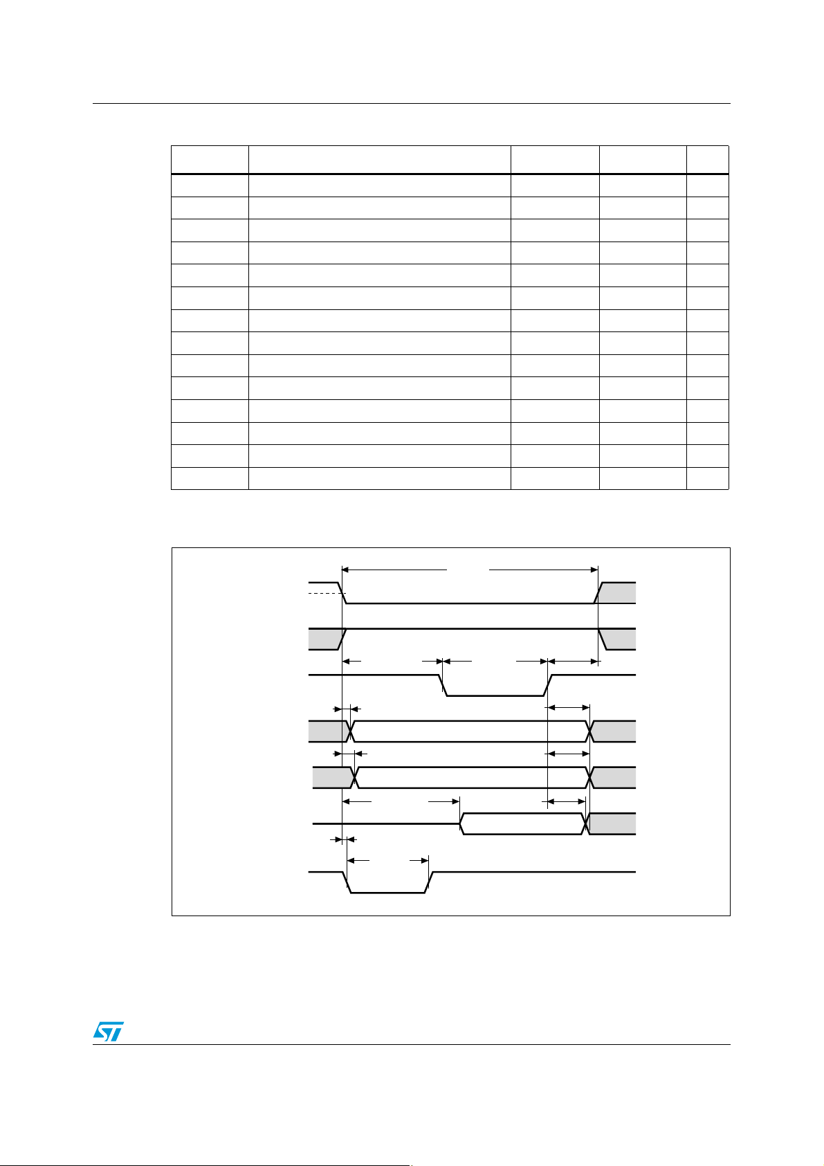
STM32F103xF, STM32F103xG Electrical characteristics
Table 31. Asynchronous non-multiplexed SRAM/PSRAM/NOR read timings
(1)
Symbol Parameter Min Max Unit
t
w(NE)
t
v(NOE_NE)
t
w(NOE)
t
h(NE_NOE)
t
v(A_NE)
t
h(A_NOE)
t
v(BL_NE)
t
h(BL_NOE)
t
su(Data_NE)
t
su(Data_NOE)
t
h(Data_NOE)
t
h(Data_NE)
t
v(NADV_NE)
t
w(NADV)
1. CL = 15 pF.
FSMC_NE low time 5t
+ 0.5 5t
HCLK
HCLK
+ 2 ns
FSMC_NEx low to FSMC_NOE low 0.5 1.5 ns
FSMC_NOE low time 5t
HCLK
– 1 5t
HCLK
+ 1 ns
FSMC_NOE high to FSMC_NE high hold time 0 - ns
FSMC_NEx low to FSMC_A valid - 3 ns
Address hold time after FSMC_NOE high 0 - ns
FSMC_NEx low to FSMC_BL valid - 0 ns
FSMC_BL hold time after FSMC_NOE high 0.5 - ns
Data to FSMC_NEx high setup time 2t
Data to FSMC_NOEx high setup time 2t
- 1 - ns
HCLK
- 1 - ns
HCLK
Data hold time after FSMC_NOE high 0 - ns
Data hold time after FSMC_NEx high 0 - ns
FSMC_NEx low to FSMC_NADV low - 0 ns
FSMC_NADV low time - t
HCLK
+ 2 ns
Figure 23. Asynchronous non-multiplexed SRAM/PSRAM/NOR write waveforms
t
w(NE)
FSMC_NEx
FSMC_NOE
Address
NBL
t
w(NWE)
t
h(BL_NWE)
t
h(Data_NWE)
t
h(A_NWE)
Data
t
h(NE_NWE)
ai14990
t
v(NWE_NE)
FSMC_NWE
t
v(A_NE)
FSMC_A[25:0]
t
v(BL_NE)
FSMC_NBL[3:0]
t
v(Data_NE)
FSMC_D[15:0]
FSMC_NADV
1. Mode 2/B, C and D only. In Mode 1, FSMC_NADV is not used.
(1)
t
v(NADV_NE)
t
w(NADV)
Doc ID 16554 Rev 3 63/120

Electrical characteristics STM32F103xF, STM32F103xG
Table 32. Asynchronous non-multiplexed SRAM/PSRAM/NOR write timings
Symbol Parameter Min Max Unit
t
w(NE)
t
v(NWE_NE)
t
w(NWE)
t
h(NE_NWE)
t
v(A_NE)
t
h(A_NWE)
t
v(BL_NE)
t
h(BL_NWE)
t
v(Data_NE)
t
h(Data_NWE)
t
v(NADV_NE)
t
w(NADV)
= 15 pF.
1. C
L
Table 33. Asynchronous read muxed
FSMC_NE low time 3t
FSMC_NEx low to FSMC_NWE low t
FSMC_NWE low time t
FSMC_NWE high to FSMC_NE high hold time t
+ 0.5 3t
HCLK
+ 0.5 t
HCLK
– 0.5 t
HCLK
– 0.5 - ns
HCLK
HCLK
HCLK
HCLK
+ 1.5 ns
+ 1.5 ns
+ 1 ns
FSMC_NEx low to FSMC_A valid - 0 ns
Address hold time after FSMC_NWE high t
HCLK
-ns
FSMC_NEx low to FSMC_BL valid - 1.5 ns
FSMC_BL hold time after FSMC_NWE high t
FSMC_NEx low to Data valid - t
Data hold time after FSMC_NWE high t
– 1.5 - ns
HCLK
HCLK
HCLK
ns
-ns
FSMC_NEx low to FSMC_NADV low - 0 ns
FSMC_NADV low time - t
HCLK
+ 1.5 ns
(1)
Symbol Parameter Min Max Unit
t
w(NE)
t
v(NOE_NE)
t
w(NOE)
t
h(NE_NOE)
t
v(A_NE)
t
v(NADV_NE)
t
w(NADV)
t
h(AD_NADV)
t
h(A_NOE)
t
h(BL_NOE)
t
v(BL_NE)
t
su(Data_NE)
t
su(Data_NOE)
t
h(Data_NE)
t
h(Data_NOE)
FSMC_NE low time 7t
FSMC_NEx low to FSMC_NOE low 3t
FSMC_NOE low time 4t
FSMC_NOE high to FSMC_NE high hold time 0.5 -
FSMC_NEx low to FSMC_A valid - 0
FSMC_NEx low to FSMC_NADV low 0 1
FSMC_NADV low time t
FSMC_AD (address) valid hold time after
FSMC NADV high
Address hold time after FSMC_NOE high t
FSMC_BL time after FSMC_NOE high 0.5 -
FSMC_NEx low to FSMC_BL valid - 0
Data to FSMC_NEx high setup time 4t
Data to FSMC_NOE high setup time 4t
Data hold time after FSMC_NEx high 0 -
Data hold time after FSMC_NOE high 0 -
+ 0.5 7t
HCLK
+ 0.5 3t
HCLK
– 1 4t
HCLK
+ 0.5 t
HCLK
t
HCLK
– 2 -
HCLK
– 0.5 -
HCLK
– 1 -
HCLK
HCLK
HCLK
HCLK
HCLK
+ 2
+ 1.5
+ 1
+ 2
-
ns
64/120 Doc ID 16554 Rev 3

STM32F103xF, STM32F103xG Electrical characteristics
NBL
Data
FSMC_NBL[1:0]
FSMC_
AD[15:0]
t
v(BL_NE)
t
h(Data_NE)
Address
FSMC_A[25:16]
t
v(A_NE)
FSMC_NWE
t
v(A_NE)
ai14892b
Address
FSMC_NADV
t
v(NADV_NE)
t
w(NADV)
t
su(Data_NE)
t
h(AD_NADV)
FSMC_NE
FSMC_NOE
t
w(NE)
t
w(NOE)
t
v(NOE_NE)
t
h(NE_NOE)
t
h(A_NOE)
t
h(BL_NOE)
t
su(Data_NOE)
t
h(Data_NOE)
Figure 24. Asynchronous multiplexed PSRAM/NOR read waveforms
Table 34. Asynchronous multiplexed PSRAM/NOR read timings
(1)
Symbol Parameter Min Max Unit
t
w(NE)
t
v(NOE_NE)
t
w(NOE)
t
h(NE_NOE)
t
v(A_NE)
t
v(NADV_NE)
t
w(NADV)
t
h(AD_NADV)
t
h(A_NOE)
t
h(BL_NOE)
t
v(BL_NE)
t
su(Data_NE)
t
su(Data_NOE)
t
h(Data_NE)
t
h(Data_NOE)
1. CL = 15 pF.
FSMC_NE low time 7t
FSMC_NEx low to FSMC_NOE low 3t
FSMC_NOE low time 4t
HCLK
HCLK
HCLK
+ 0.5 7t
+ 0.5 3t
– 1 4t
FSMC_NOE high to FSMC_NE high hold time 0.5 - ns
FSMC_NEx low to FSMC_A valid - 0 ns
FSMC_NEx low to FSMC_NADV low 0 1 ns
FSMC_NADV low time t
FSMC_AD (address) valid hold time after
FSMC_NADV high
Address hold time after FSMC_NOE high t
+ 0.5 t
HCLK
t
HCLK
-2 - ns
HCLK
FSMC_BL hold time after FSMC_NOE high 0.5 - ns
FSMC_NEx low to FSMC_BL valid - 0 ns
Data to FSMC_NEx high setup time 4t
Data to FSMC_NOE high setup time 4t
Data hold time after FSMC_NEx high 0 - ns
Data hold time after FSMC_NOE high 0 - ns
- 0.5 - ns
HCLK
- 1 - ns
Doc ID 16554 Rev 3 65/120
HCLK
+ 2 ns
HCLK
+ 1.5 ns
HCLK
+ 1 ns
HCLK
+ 2 ns
HCLK
- ns

Electrical characteristics STM32F103xF, STM32F103xG
NBL
Data
FSMC_NEx
FSMC_NBL[1:0]
FSMC_
AD[15:0]
t
v(BL_NE)
t
h(Data_NWE)
FSMC_NOE
Address
FSMC_A[25:16]
t
v(A_NE)
t
w(NWE)
FSMC_NWE
t
v(NWE_NE)
t
h(NE_NWE)
t
h(A_NWE)
t
h(BL_NWE)
t
v(A_NE)
t
w(NE)
ai14891B
Address
FSMC_NADV
t
v(NADV_NE)
t
w(NADV)
t
v(Data_NADV)
t
h(AD_NADV)
Figure 25. Asynchronous multiplexed PSRAM/NOR write waveforms
66/120 Doc ID 16554 Rev 3
Table 35. Asynchronous multiplexed PSRAM/NOR write timings
(1)
Symbol Parameter Min Max Unit
t
w(NE)
t
v(NWE_NE)
t
w(NWE)
t
h(NE_NWE)
t
v(A_NE)
t
v(NADV_NE)
t
w(NADV)
t
h(AD_NADV)
t
h(A_NWE)
t
v(BL_NE)
t
h(BL_NWE)
t
v(Data_NADV)
t
h(Data_NWE)
1. C
= 15 pF.
L
FSMC_NE low time 5t
FSMC_NEx low to FSMC_NWE low t
FSMC_NWE low time 3t
FSMC_NWE high to FSMC_NE high hold time t
FSMC_NEx low to FSMC_A valid - 3.5 ns
FSMC_NEx low to FSMC_NADV low 0 1 ns
FSMC_NADV low time t
FSMC_AD (address) valid hold time after
FSMC_NADV high
Address hold time after FSMC_NWE high 4t
FSMC_NEx low to FSMC_BL valid - 0.5 ns
FSMC_BL hold time after FSMC_NWE high t
FSMC_NADV high to Data valid - t
Data hold time after FSMC_NWE high t
+ 0.5 5t
HCLK
+ 1 t
HCLK
+ 0.5 3t
HCLK
– 0.5 - ns
HCLK
+ 0.5 t
HCLK
t
– 0.5 - ns
HCLK
– 2 - ns
HCLK
– 1.5 - ns
HCLK
– 0.5 - ns
HCLK
HCLK
HCLK
HCLK
HCLK
HCLK
+ 2 ns
+ 1.5 ns
+ 1 ns
+ 1.5 ns
+ 6 ns

STM32F103xF, STM32F103xG Electrical characteristics
Synchronous waveforms and timings
Figure 26 through Figure 29 represent synchronous waveforms and Ta bl e 37 through
Ta bl e 39 provide the corresponding timings. The results shown in these tables are obtained
with the following FSMC configuration:
● BurstAccessMode = FSMC_BurstAccessMode_Enable;
● MemoryType = FSMC_MemoryType_CRAM;
● WriteBurst = FSMC_WriteBurst_Enable;
● CLKDivision = 1; (0 is not supported, see the STM32F10xxx reference manual)
● DataLatency = 1 for NOR Flash; DataLatency = 0 for PSRAM
Figure 26. Synchronous multiplexed NOR/PSRAM read timings
T
W#,+
&3-#?#,+
&3-#?.%X
T
D#,+,.!$6,
&3-#?.!$6
&3-#?!;=
&3-#?./%
T
T
D#,+,!$6
&3-#?!$;=
&3-#?.7!)4
7!)4#&'B7!)40/,B
&3-#?.7!)4
7!)4#&'B7!)40/,B
T
W#,+
$ATALATENCY
T
D#,+,.%X,
T
D#,+,.!$6(
T
D#,+,!6
T
D#,+,./%,
D#,+,!$)6
T
SU!$6#,+(
T
H#,+(!$6
T
SU!$6#,+(
!$;= $ $
T
SU.7!)46#,+(
T
SU.7!)46#,+(
T
SU.7!)46#,+(
T
H#,+(.7!)46
T
H#,+(.7!)46
"53452.
T
D#,+,.%X(
T
D#,+,!)6
T
D#,+,./%(
T
H#,+(!$6
$
T
H#,+(.7!)46
AIH
Doc ID 16554 Rev 3 67/120

Electrical characteristics STM32F103xF, STM32F103xG
Table 36. Synchronous multiplexed NOR/PSRAM read timings
(1)
Symbol Parameter Min Max Unit
t
w(CLK)
t
d(CLKL-NExL)
t
d(CLKL-NExH)
t
d(CLKL-NADVL)
t
d(CLKL-NADVH)
t
d(CLKL-AV)
t
d(CLKL-AIV)
t
d(CLKL-NOEL)
t
d(CLKL-NOEH)
t
d(CLKL-ADV)
t
d(CLKL-ADIV)
t
su(ADV-CLKH)
t
h(CLKH-ADV)
1. CL = 15 pF.
FSMC_CLK period 27.6 - ns
FSMC_CLK low to FSMC_NEx low (x = 0...2) - 0.5 ns
FSMC_CLK low to FSMC_NEx high (x = 0...2) 1 - ns
FSMC_CLK low to FSMC_NADV low - 1 ns
FSMC_CLK low to FSMC_NADV high 0.5 - ns
FSMC_CLK low to FSMC_Ax valid (x = 0...25) - 0 ns
FSMC_CLK low to FSMC_Ax invalid (x = 16...25) 1.5 - ns
FSMC_CLK low to FSMC_NOE low - 14 ns
FSMC_CLK low to FSMC_NOE high 1 - ns
FSMC_CLK low to FSMC_AD[15:0] valid - 11 ns
FSMC_CLK low to FSMC_AD[15:0] invalid 0.5 - ns
FSMC_A/D[15:0] valid data before FSMC_CLK
high
2- ns
FSMC_A/D[15:0] valid data after FSMC_CLK high 0 - ns
68/120 Doc ID 16554 Rev 3

STM32F103xF, STM32F103xG Electrical characteristics
Figure 27. Synchronous multiplexed PSRAM write timings
"53452.
&3-#?#,+
T
W#,+
T
W#,+
T
D#,+,.%X,
T
D#,+,.%X(
&3-#?.%X
$ATALATENCY
T
D#,+,.!$6,
T
D#,+,.!$6(
&3-#?.!$6
T
D#,+,!6
&3-#?!;=
T
D#,+,.7%,
T
D#,+,.7%(
&3-#?.7%
T
D#,+,!$6
T
D#,+,!$)6
T
D#,+,$ATA
T
D#,+,$ATA
&3-#?!$;= !$;= $ $
&3-#?.7!)4
7!)4#&'B7!)40/,B
T
SU.7!)46#,+(
T
H#,+(.7!)46
T
D#,+,.",(
&3-#?.",
T
D#,+,!)6
AIG
Doc ID 16554 Rev 3 69/120

Electrical characteristics STM32F103xF, STM32F103xG
Table 37. Synchronous multiplexed PSRAM write timings
(1)
Symbol Parameter Min Max Unit
t
w(CLK)
t
d(CLKL-NExL)
t
d(CLKL-NExH)
t
d(CLKL-NADVL)
t
d(CLKL-NADVH)
t
d(CLKL-AV)
t
d(CLKL-AIV)
t
d(CLKL-NWEL)
t
d(CLKL-NWEH)
t
d(CLKL-ADV)
t
d(CLKL-ADIV)
t
d(CLKL-Data)
t
d(CLKL-NBLH)
= 15 pF.
1. C
L
FSMC_CLK period 27.5 - ns
FSMC_CLK low to FSMC_Nex low (x = 0...2) - 0 ns
FSMC_CLK low to FSMC_NEx high (x = 0...2) 1 - ns
FSMC_CLK low to FSMC_NADV low - 1 ns
FSMC_CLK low to FSMC_NADV high 1 - ns
FSMC_CLK low to FSMC_Ax valid (x = 16...25) - 0 ns
FSMC_CLK low to FSMC_Ax invalid (x = 16...25) 1 - ns
FSMC_CLK low to FSMC_NWE low - 1 ns
FSMC_CLK low to FSMC_NWE high 1.5 - ns
FSMC_CLK low to FSMC_AD[15:0] valid - 10 ns
FSMC_CLK low to FSMC_AD[15:0] invalid 1 - ns
FSMC_A/D[15:0] valid after FSMC_CLK low - 6 ns
FSMC_CLK low to FSMC_NBL high 1 - ns
70/120 Doc ID 16554 Rev 3

STM32F103xF, STM32F103xG Electrical characteristics
&3-#?#,+
&3-#?.%X
&3-#?!;=
&3-#?./%
&3-#?$;=
$ $
&3-#?.7!)4
7!)4#&'B7!)40/,B
&3-#?.7!)4
7!)4#&'B7!)40/,B
T
W#,+
T
W#,+
$ATALATENCY
"53452.
T
D#,+,.%X,
T
D#,+,.%X(
T
D#,+,!6
T
D#,+,!)6
T
D#,+,./%,
T
D#,+,./%(
T
SU$6#,+(
T
H#,+($6
T
SU$6#,+(
T
H#,+($6
T
SU.7!)46#,+(
T
H#,+(.7!)46
T
SU.7!)46#,+(
T
H#,+(.7!)46
T
SU.7!)46#,+(
T
H#,+(.7!)46
AIG
&3-#?.!$6
T
D#,+,.!$6,
T
D#,+,.!$6(
$
Figure 28. Synchronous non-multiplexed NOR/PSRAM read timings
Table 38. Synchronous non-multiplexed NOR/PSRAM read timings
Symbol Parameter Min Max Unit
t
w(CLK)
t
d(CLKL-NExL)
t
d(CLKL-NExH)
t
d(CLKL-NADVL)
t
d(CLKL-NADVH)
t
d(CLKL-AV)
t
d(CLKL-AIV)
t
d(CLKL-NOEL)
t
d(CLKL-NOEH)
t
su(DV-CLKH)
t
h(CLKH-DV)
1. CL = 15 pF.
FSMC_CLK period 27.6 - ns
FSMC_CLK low to FSMC_NEx low (x = 0...2) - 1.5 ns
FSMC_CLK low to FSMC_NEx high (x = 0...2) 2 - ns
FSMC_CLK low to FSMC_NADV low - 0.5 ns
FSMC_CLK low to FSMC_NADV high 1 - ns
FSMC_CLK low to FSMC_Ax valid (x = 0...25) - 0 ns
FSMC_CLK low to FSMC_Ax invalid (x = 0...25) 2 - ns
FSMC_CLK low to FSMC_NOE low - t
FSMC_CLK low to FSMC_NOE high 1.5 - ns
FSMC_D[15:0] valid data before FSMC_CLK high 3.5 - ns
FSMC_D[15:0] valid data after FSMC_CLK high 0 - ns
Doc ID 16554 Rev 3 71/120
(1)
HCLK
+ 1 ns

Electrical characteristics STM32F103xF, STM32F103xG
&3-#?#,+
&3-#?.%X
&3-#?!;=
&3-#?.7%
&3-#?$;=
$ $
&3-#?.7!)4
7!)4#&'B7!)40/,B
T
W#,+
T
W#,+
$ATALATENCY
"53452.
T
D#,+,.%X,
T
D#,+,.%X(
T
D#,+,!6
T
D#,+,!)6
T
D#,+,.7%(
T
D#,+,.7%,
T
D#,+,$ATA
T
SU.7!)46#,+(
T
H#,+(.7!)46
AIH
&3-#?.!$6
T
D#,+,.!$6,
T
D#,+,.!$6(
T
D#,+,$ATA
&3-#?.",
T
D#,+,.",(
Figure 29. Synchronous non-multiplexed PSRAM write timings
Table 39. Synchronous non-multiplexed PSRAM write timings
Symbol Parameter Min Max Unit
FSMC_CLK period 27.6 - ns
FSMC_CLK low to FSMC_NEx low (x = 0...2) - 0.5 ns
FSMC_CLK low to FSMC_NEx high (x = 0...2) 1.5 - ns
FSMC_CLK low to FSMC_NADV low - 1 ns
FSMC_CLK low to FSMC_NADV high 0.5 - ns
FSMC_CLK low to FSMC_Ax valid (x = 16...25) - 0 ns
FSMC_CLK low to FSMC_Ax invalid (x = 16...25) 1.5 - ns
FSMC_CLK low to FSMC_NWE low - 1 ns
FSMC_CLK low to FSMC_NWE high 1.5 - ns
FSMC_D[15:0] valid data after FSMC_CLK low - 2.5 ns
FSMC_CLK low to FSMC_NBL high 0.5 - ns
t
w(CLK)
t
d(CLKL-NExL)
t
d(CLKL-NExH)
t
d(CLKL-NADVL)
t
d(CLKL-NADVH)
t
d(CLKL-AV)
t
d(CLKL-AIV)
t
d(CLKL-NWEL)
t
d(CLKL-NWEH)
t
d(CLKL-Data)
t
d(CLKL-NBLH)
1. CL = 15 pF.
72/120 Doc ID 16554 Rev 3
(1)

STM32F103xF, STM32F103xG Electrical characteristics
PC Card/CompactFlash controller waveforms and timings
Figure 30 through Figure 35 represent synchronous waveforms and Ta bl e 42 provides the
corresponding timings. The results shown in this table are obtained with the following FSMC
configuration:
● COM.FSMC_SetupTime = 0x04;
● COM.FSMC_WaitSetupTime = 0x07;
● COM.FSMC_HoldSetupTime = 0x04;
● COM.FSMC_HiZSetupTime = 0x00;
● ATT.FSMC_SetupTime = 0x04;
● ATT.FSMC_WaitSetupTime = 0x07;
● ATT.FSMC_HoldSetupTime = 0x04;
● ATT.FSMC_HiZSetupTime = 0x00;
● IO.FSMC_SetupTime = 0x04;
● IO.FSMC_WaitSetupTime = 0x07;
● IO.FSMC_HoldSetupTime = 0x04;
● IO.FSMC_HiZSetupTime = 0x00;
● TCLRSetupTime = 0;
● TARSetupTime = 0;
Figure 30. PC Card/CompactFlash controller waveforms for common memory read
access
FSMC_NCE4_2
FSMC_NCE4_1
FSMC_A[10:0]
FSMC_NREG
FSMC_NIOWR
FSMC_NIORD
FSMC_NWE
FSMC_N
FSMC_D[15:0]
1. FSMC_NCE4_2 remains high (inactive during 8-bit access.
(1)
t
d(NCE4_1-NOE)
OE
t
v(NCEx-A)
t
d(NREG-NCEx)
t
d(NIORD-NCEx)
t
w(NOE)
t
su(D-NOE)
t
h(NCEx-AI)
t
h(NCEx-NREG)
t
h(NCEx-NIORD)
t
h(NCEx-
NIOWR
t
h(NOE-D)
)
ai14895b
Doc ID 16554 Rev 3 73/120

Electrical characteristics STM32F103xF, STM32F103xG
t
d(NCE4_1-NWE)
t
w(NWE)
t
h(NWE-D)
t
v(NCE4_1-A)
t
d(NREG-NCE4_1)
t
d(NIORD-NCE4_1)
t
h(NCE4_1-AI)
MEMxHIZ =1
t
v(NWE-D)
t
h(NCE4_1-NREG)
t
h(NCE4_1-NIORD)
t
h(NCE4_1-NIOWR)
ai14896b
FSMC_NWE
FSMC_N
OE
FSMC_D[15:0]
FSMC_A[10:0]
FSMC_NCE4_1
FSMC_NREG
FSMC_NIOWR
FSMC_NIORD
t
d(NWE-NCE4_1)
t
d(D-NWE)
FSMC_NCE4_2
High
Figure 31. PC Card/CompactFlash controller waveforms for common memory write
access
74/120 Doc ID 16554 Rev 3

STM32F103xF, STM32F103xG Electrical characteristics
t
d(NCE4_1-NOE)
t
w(NOE)
t
su(D-NOE)
t
h(NOE-D)
t
v(NCE4_1-A)
t
h(NCE4_1-AI)
t
d(NREG-NCE4_1)
t
h(NCE4_1-NREG)
ai14897b
FSMC_NWE
FSMC_NOE
FSMC_D[15:0]
(1)
FSMC_A[10:0]
FSMC_NCE4_2
FSMC_NCE4_1
FSMC_NREG
FSMC_NIOWR
FSMC_NIORD
t
d(NOE-NCE4_1)
High
Figure 32. PC Card/CompactFlash controller waveforms for attribute memory read
access
1. Only data bits 0...7 are read (bits 8...15 are disregarded).
Doc ID 16554 Rev 3 75/120

Electrical characteristics STM32F103xF, STM32F103xG
Figure 33. PC Card/CompactFlash controller waveforms for attribute memory write
access
FSMC_NCE4_1
FSMC_NCE4_2
High
t
v(NCE4_1-A)
t
h(NCE4_1-AI)
FSMC_A[10:0]
FSMC_NIOWR
FSMC_NIORD
t
d(NREG-NCE4_1)
t
h(NCE4_1-NREG)
FSMC_NREG
t
d(NCE4_1-NWE)
t
w(NWE)
FSMC_NWE
t
d(NWE-NCE4_1)
FSMC_NOE
t
v(NWE-D)
FSMC_D[7:0](1)
ai14898b
1. Only data bits 0...7 are driven (bits 8...15 remains HiZ).
Figure 34. PC Card/CompactFlash controller waveforms for I/O space read access
FSMC_NCE4_1
FSMC_NCE4_2
t
v(NCEx-A)
FSMC_A[10:0]
FSMC_NREG
FSMC_NWE
FSMC_NOE
FSMC_NIOWR
t
d(NIORD-NCE4_1)
FSMC_NIORD
FSMC_D[15:0]
76/120 Doc ID 16554 Rev 3
t
su(D-NIORD)
t
h(NCE4_1-AI)
t
w(NIORD)
t
d(NIORD-D)
ai14899B

STM32F103xF, STM32F103xG Electrical characteristics
T
D.#%?.)/72
T
W.)/72
T
V.#%X!
T
H.#%?!)
T
H.)/72$
!44X():
T
V.)/72$
AIB
&3-#?.7%
&3-#?./%
&3-#?$;=
&3-#?!;=
&3-#?.#%?
&3-#?.#%?
&3-#?.2%'
&3-#?.)/72
&3-#?.)/2$
Figure 35. PC Card/CompactFlash controller waveforms for I/O space write access
Table 40. Switching characteristics for PC Card/CF read and write cycles in
attribute/common space
Symbol Parameter Min Max Unit
t
v(NCEx-A)
t
h(NCEx-AI)
t
d(NREG-NCEx)
t
h(NCEx-NREG)
t
d(NCEx_NWE)
t
d(NCEx_NOE)
t
w(NOE)
t
d(NOE-NCEx
t
su(D-NOE)
t
h(NOE-D)
t
w(NWE)
t
d(NWE_NCEx)
t
d(NCEx-NWE)
t
v(NWE-D)
t
h(NWE-D)
t
d(D-NWE)
FSMC_NCEx low to FSMC_Ay valid - 0
FSMC_NCEx high to FSMC_Ax invalid 0 -
FSMC_NCEx low to FSMC_NREG valid - 2
FSMC_NCEx high to FSMC_NREG invalid t
+ 4 -
HCLK
FSMC_NCEx low to FSMC_NWE low - 5t
FSMC_NCEx low to FSMC_NOE low - 5t
FSMC_NOE low width 8t
FSMC_NOE high to FSMC_NCEx high 5t
- 0.5 8t
HCLK
- 0.5 -
HCLK
FSMC_D[15:0] valid data before FSMC_NOE high 32 -
FSMC_NOE high to FSMC_D[15:0] invalid t
FSMC_NWE low width 8t
FSMC_NWE high to FSMC_NCEx high 5t
HCLK
– 1 8t
HCLK
+ 1.5 -
HCLK
FSMC_NCEx low to FSMC_NWE low - 5t
FSMC_NWE low to FSMC_D[15:0] valid - 0
FSMC_NWE high to FSMC_D[15:0] invalid 11t
FSMC_D[15:0] valid before FSMC_NWE high 13t
HCLK
+ 2.5 -
HCLK
HCLK
HCLK
HCLK
-
HCLK
HCLK
-
+ 1
+ 1
+ 1
ns
+ 4
+ 1
Doc ID 16554 Rev 3 77/120

Electrical characteristics STM32F103xF, STM32F103xG
Table 41. Switching characteristics for PC Card/CF read and write cycles in I/O space
Symbol Parameter Min Max Unit
tw
(NIOWR)
tv
(NIOWR-D)
th
(NIOWR-D)
td
(NCE4_1-NIOWR)
th
(NCEx-NIOWR)
td
(NIORD-NCEx)
th
(NCEx-NIORD)
tw
(NIORD)
tsu
(D-NIORD)
td
(NIORD-D)
FSMC_NIOWR low width 8 THCLK - ns
FSMC_NIOWR low to FSMC_D[15:0] valid -
FSMC_NIOWR high to FSMC_D[15:0] invalid
11THCLK -
FSMC_NCE4_1 low to FSMC_NIOWR valid -
FSMC_NCEx high to FSMC_NIOWR invalid
5THCLK -
2.5
FSMC_NCEx low to FSMC_NIORD valid -
FSMC_NCEx high to FSMC_NIORD) valid
5 THCLK -
0.5
7
5 THCLK -
4
-ns
5THCLK +
1
-ns
5THCLK -
0.5
-ns
FSMC_NIORD low width 8THCLK - ns
FSMC_D[15:0] valid before FSMC_NIORD high 28 ns
FSMC_D[15:0] valid after FSMC_NIORD high 3 ns
ns
ns
ns
NAND controller waveforms and timings
Figure 36 through Figure 39 represent synchronous waveforms and Ta bl e 43 provides the
corresponding timings. The results shown in this table are obtained with the following FSMC
configuration:
● COM.FSMC_SetupTime = 0x00;
● COM.FSMC_WaitSetupTime = 0x02;
● COM.FSMC_HoldSetupTime = 0x01;
● COM.FSMC_HiZSetupTime = 0x00;
● ATT.FSMC_SetupTime = 0x00;
● ATT.FSMC_WaitSetupTime = 0x02;
● ATT.FSMC_HoldSetupTime = 0x01;
● ATT.FSMC_HiZSetupTime = 0x00;
● Bank = FSMC_Bank_NAND;
● MemoryDataWidth = FSMC_MemoryDataWidth_16b;
● ECC = FSMC_ECC_Enable;
● ECCPageSize = FSMC_ECCPageSize_512Bytes;
● TCLRSetupTime = 0;
● TARSetupTime = 0;
78/120 Doc ID 16554 Rev 3

STM32F103xF, STM32F103xG Electrical characteristics
FSMC_NWE
FSMC_NOE (NRE)
FSMC_D[15:0]
t
su(D-NOE)
t
h(NOE-D)
ai14901b
ALE (FSMC_A17)
CLE (FSMC_A16)
FSMC_NCEx
Low
t
d(ALE-NOE)th(NOE-ALE)
t
h(NWE-D)
t
v(NWE-D)
ai14902b
FSMC_NWE
FSMC_NOE (NRE)
FSMC_D[15:0]
ALE (FSMC_A17)
CLE (FSMC_A16)
FSMC_NCEx
Low
t
d(ALE-NWE)th(NWE-ALE)
Figure 36. NAND controller waveforms for read access
Figure 37. NAND controller waveforms for write access
Figure 38. NAND controller waveforms for common memory read access
FSMC_NCEx
ALE (FSMC_A17)
CLE (FSMC_A16)
FSMC_NWE
FSMC_N
FSMC_D[15:0]
Low
OE
t
d(ALE-NOE)
t
w(NOE)
t
su(D-NOE)
t
h(NOE-ALE)
t
h(NOE-D)
Doc ID 16554 Rev 3 79/120
ai14912b

Electrical characteristics STM32F103xF, STM32F103xG
t
w(NWE)
t
h(NWE-D)
t
v(NWE-D)
ai14913b
FSMC_NWE
FSMC_N
OE
FSMC_D[15:0]
t
d(D-NWE)
ALE (FSMC_A17)
CLE (FSMC_A16)
FSMC_NCEx
Low
t
d(ALE-NOE)
t
h(NOE-ALE)
Figure 39. NAND controller waveforms for common memory write access
Table 42. Switching characteristics for NAND Flash read cycles
(1)
Symbol Parameter Min Max Unit
t
w(NOE)
t
su(D-NOE)
t
h(NOE-D)
t
d(ALE-NOE)
t
h(NOE-ALE)
1. C
= 15 pF.
L
Table 43. Switching characteristics for NAND Flash write cycles
FSMC_NOE low width 3t
FSMC_D[15:0] valid data before FSMC_NOE
high
FSMC_D[15:0] valid data after FSMC_NOE high 0 - ns
FSMC_ALE valid before FSMC_NOE low - 2t
FSMC_NWE high to FSMC_ALE invalid 2t
HCLK
– 1 3t
HCLK
+ 1 ns
13 - ns
HCLK
HCLK
(1)
- ns
Symbol Parameter Min Max Unit
t
w(NWE)
t
v(NWE-D)
t
h(NWE-D)
t
d(ALE-NWE)
t
h(NWE-ALE)
t
d(ALE-NOE)
t
h(NOE-ALE)
1. C
= 15 pF.
L
FSMC_NWE low width 3t
HCLK
3t
HCLK
FSMC_NWE low to FSMC_D[15:0] valid - 0 ns
FSMC_NWE high to FSMC_D[15:0] invalid 2t
FSMC_ALE valid before FSMC_NWE low - 3t
FSMC_NWE high to FSMC_ALE invalid 3t
FSMC_ALE valid before FSMC_NOE low - 2t
FSMC_NWE high to FSMC_ALE invalid 2t
+ 2 - ns
HCLK
HCLK
+ 8 - ns
HCLK
HCLK
HCLK
- ns
+ 1.5 ns
ns
ns
ns
80/120 Doc ID 16554 Rev 3

STM32F103xF, STM32F103xG Electrical characteristics
5.3.11 EMC characteristics
Susceptibility tests are performed on a sample basis during device characterization.
Functional EMS (electromagnetic susceptibility)
While a simple application is executed on the device (toggling 2 LEDs through I/O ports). the
device is stressed by two electromagnetic events until a failure occurs. The failure is
indicated by the LEDs:
● Electrostatic discharge (ESD) (positive and negative) is applied to all device pins until
a functional disturbance occurs. This test is compliant with the IEC 61000-4-2 standard.
● FTB: A Burst of Fast Transient voltage (positive and negative) is applied to V
V
through a 100 pF capacitor, until a functional disturbance occurs. This test is
SS
compliant with the IEC 61000-4-4 standard.
A device reset allows normal operations to be resumed.
The test results are given in Tab l e 44. They are based on the EMS levels and classes
defined in application note AN1709.
Table 44. EMS characteristics
DD
and
Symbol Parameter Conditions
= 3.3 V, LQFP144, TA = +25 °C,
V
V
V
FESD
EFTB
Voltage limits to be applied on any I/O pin to
induce a functional disturbance
Fast transient voltage burst limits to be
applied through 100 pF on VDD and V
SS
pins to induce a functional disturbance
DD
f
= 72 MHz
HCLK
conforms to IEC 61000-4-2
V
= 3.3 V, LQFP144, TA = +25 °C,
DD
f
= 72 MHz
HCLK
conforms to IEC 61000-4-4
Level/
Class
2B
4A
Designing hardened software to avoid noise problems
EMC characterization and optimization are performed at component level with a typical
application environment and simplified MCU software. It should be noted that good EMC
performance is highly dependent on the user application and the software in particular.
Therefore it is recommended that the user applies EMC software optimization and
prequalification tests in relation with the EMC level requested for his application.
Software recommendations
The software flowchart must include the management of runaway conditions such as:
● Corrupted program counter
● Unexpected reset
● Critical Data corruption (control registers...)
Doc ID 16554 Rev 3 81/120

Electrical characteristics STM32F103xF, STM32F103xG
Prequalification trials
Most of the common failures (unexpected reset and program counter corruption) can be
reproduced by manually forcing a low state on the NRST pin or the Oscillator pins for 1
second.
To complete these trials, ESD stress can be appFlied directly on the device, over the range
of specification values. When unexpected behavior is detected, the software can be
hardened to prevent unrecoverable errors occurring (see application note AN1015).
Electromagnetic Interference (EMI)
The electromagnetic field emitted by the device are monitored while a simple application is
executed (toggling 2 LEDs through the I/O ports). This emission test is compliant with
IEC
61967-2 standard which specifies the test board and the pin loading.
Table 45. EMI characteristics
Symbol Parameter Conditions
Monitored
frequency band
0.1 to 30 MHz 8 12
= 3.3 V, TA = 25 °C,
V
DD
S
EMI
Peak level
LQFP144 package
compliant with IEC
61967-2
130 MHz to 1GHz 28 33
SAE EMI Level 4 4 -
5.3.12 Absolute maximum ratings (electrical sensitivity)
Based on three different tests (ESD, LU) using specific measurement methods, the device is
stressed in order to determine its performance in terms of electrical sensitivity.
Electrostatic discharge (ESD)
Electrostatic discharges (a positive then a negative pulse separated by 1 second) are
applied to the pins of each sample according to each pin combination. The sample size
depends on the number of supply pins in the device (3 parts × (n+1) supply pins). This test
conforms to the JESD22-A114/C101 standard.
Table 46. ESD absolute maximum ratings
Symbol Ratings Conditions Class Maximum value
Max vs. [f
HSE/fHCLK
8/48 MHz 8/72 MHz
]
Unit
dBµV30 to 130 MHz 31 21
(1)
Unit
V
ESD(HBM)
V
ESD(CDM)
1. Based on characterization results, not tested in production.
Electrostatic discharge
voltage (human body model)
Electrostatic discharge
voltage (charge device model)
82/120 Doc ID 16554 Rev 3
TA = +25 °C, conforming
to JESD22-A114
TA = +25 °C, conforming
to JESD22-C101
22000
V
II 500

STM32F103xF, STM32F103xG Electrical characteristics
Static latch-up
Two complementary static tests are required on six parts to assess the latch-up
performance:
● A supply overvoltage is applied to each power supply pin
● A current injection is applied to each input, output and configurable I/O pin
These tests are compliant with EIA/JESD 78A IC latch-up standard.
Table 47. Electrical sensitivities
Symbol Parameter Conditions Class
LU Static latch-up class T
= +105 °C conforming to JESD78A II level A
A
5.3.13 I/O current injection characteristics
As a general rule, current injection to the I/O pins, due to external voltage below VSS or
above V
operation. However, in order to give an indication of the robustness of the microcontroller in
cases when abnormal injection accidentally happens, susceptibility tests are performed on a
sample basis during device characterization.
Functional susceptibilty to I/O current injection
While a simple application is executed on the device, the device is stressed by injecting
current into the I/O pins programmed in floating input mode. While current is injected into the
I/O pin, one at a time, the device is checked for functional failures.
The failure is indicated by an out of range parameter: ADC error above a certain limit (>5
LSB TUE), out of spec current injection on adjacent pins or other functional failure (for
example reset, oscillator frequency deviation).
The test results are given in Tab l e 48
Table 48. I/O current injection susceptibility
Symbol Description
(for standard, 3 V-capable I/O pins) should be avoided during normal product
DD
Functional susceptibility
Negative
injection
Positive
injection
Unit
I
INJ
Injected current on OSC_IN32,
OSC_OUT32, PA4, PA5, PC13
Injected current on all FT pins -5 +0
-0 +0
mA
Injected current on any other pin -5 +5
Doc ID 16554 Rev 3 83/120

Electrical characteristics STM32F103xF, STM32F103xG
5.3.14 I/O port characteristics
General input/output characteristics
Unless otherwise specified, the parameters given in Ta bl e 49 are derived from tests
performed under the conditions summarized in Tab l e 10. All I/Os are CMOS and TTL
compliant.
Table 49. I/O static characteristics
Symbol Parameter Conditions Min Typ
Max Unit
Standard IO input low
level voltage
V
IL
IO FT
(1)
voltage
Standard IO input high
level voltage
V
IH
IO FT
(1)
voltage
input low level
input high level
–0.3 -
–0.3 -
0.41*(VDD-2
V)+1.3 V
> 2 V
V
DD
V
≤ 2 V 5.2
DD
0.42*(V
V)+1 V
DD
-2
-V
-
0.28*(VDD-2
V)+0.8 V
DD
-2
0.32*(V
V)+0.75 V
+0.3 V
DD
5.5
Standard IO Schmitt
trigger voltage
hys
hysteresis
V
IO FT Schmitt trigger
voltage hysteresis
I
Input leakage current
lkg
R
R
1. FT = Five-volt tolerant. In order to sustain a voltage higher than VDD+0.3 the internal pull-up/pull-down resistors must be
2. Hysteresis voltage between Schmitt trigger switching levels. Based on characterization, not tested in production.
3. With a minimum of 100 mV.
4. Leakage could be higher than max. if negative current is injected on adjacent pins.
5. Pull-up and pull-down resistors are designed with a true resistance in series with a switchable PMOS/NMOS. This
Weak pull-up equivalent
PU
resistor
Weak pull-down
PD
equivalent resistor
I/O pin capacitance - 5 - pF
C
IO
disabled.
MOS/NMOS contribution
(5)
(2)
(2)
V
≤ V
SS
(4)
Standard I/Os
V
IN
(5)
to the series resistance is minimum (~10% order).
≤ V
IN
DD
= 5 V, I/O FT - - 3
V
= V
IN
SS
V
= V
IN
DD
200 - - mV
5% V
(3) -
DD
-mV
--±1
30 40 50 kΩ
30 40 50 kΩ
V
V
V
µA
All I/Os are CMOS and TTL compliant (no software configuration required). Their
characteristics cover more than the strict CMOS-technology or TTL parameters. The
coverage of these requirements is shown in
84/120 Doc ID 16554 Rev 3
in Figure 42 and Figure 43 for 5 V tolerant I/Os.
Figure 40 and Figure 41 for standard I/Os, and

STM32F103xF, STM32F103xG Electrical characteristics
AIB
6$$6
)NPUTRANGE
NOTGUARANTEED
6
)(
6
$$
#-/3STANDARDREQUIREMENT6
)(
6
$$
6)(6),6
#-/3STANDARDREQUIREMENT6
),
6
$$
6
),
6
##
7
),MAX
7
)(MIN
AI
)NPUTRANGE
NOTGUARANTEED
6)(6),6
44,REQUIREMENTS 6)(6
6
)(
6
$$
6
),
6
$$
44,REQUIREMENTS 6),6
6$$6
7
),MAX
7
)(MIN
Figure 40. Standard I/O input characteristics - CMOS port
Figure 41. Standard I/O input characteristics - TTL port
Doc ID 16554 Rev 3 85/120

Electrical characteristics STM32F103xF, STM32F103xG
6$$
#-/3STANDARDREQUIREMENTS6
)(
6
$$
#-/3STANDARDREQUIRMENT6
),
6
$$
6)(6),6
6$$6
)NPUTRANGE
NOTGUARANTEED
AIB
6
)(
6
$$
6
),
6
$$
NOTGUARANTEED
)NPUTRANGE
44,REQUIREMENT6)(6
6
)(
6
$$
6
),
6
$$
44,REQUIREMENTS6),6
6)(6),6
6$$6
7
),MAX
7
)(MIN
AI
Figure 42. 5 V tolerant I/O input characteristics - CMOS port
Figure 43. 5 V tolerant I/O input characteristics - TTL port
Output driving current
The GPIOs (general purpose input/outputs) can sink or source up to ±8 mA, and sink or
source up to ± 20 mA (with a relaxedV
or source up to ±3 mA. When using the GPIOs PC13 to PC15 in output mode, the speed
should not exceed 2 MHz with a maximum load of 30 pF.
In the user application, the number of I/O pins which can drive current must be limited to
respect the absolute maximum rating specified in
● The sum of the currents sourced by all the I/Os on V
consumption of the MCU sourced on V
I
(see Ta b le 8 ).
VDD
● The sum of the currents sunk by all the I/Os on V
consumption of the MCU sunk on V
I
(see Ta b le 8 ).
VSS
86/120 Doc ID 16554 Rev 3
OL/VOH
) except PC13, PC14 and PC15 which can sink
Section 5.2:
plus the maximum Run
cannot exceed the absolute maximum rating
DD,
cannot exceed the absolute maximum rating
SS
DD,
plus the maximum Run
SS

STM32F103xF, STM32F103xG Electrical characteristics
Output voltage levels
Unless otherwise specified, the parameters given in Ta bl e 50 are derived from tests
performed under ambient temperature and VDD supply voltage conditions summarized in
Ta bl e 10. All I/Os are CMOS and TTL compliant.
Table 50. Output voltage characteristics
Symbol Parameter Conditions Min Max Unit
Output low level voltage for an I/O pin
(1)
V
OL
V
OH
V
OL
V
OH
V
OL
V
OH
V
OL
V
OH
when 8 pins are sunk at same time
Output high level voltage for an I/O pin
(2)
when 8 pins are sourced at same time
Output low level voltage for an I/O pin
(1)
when 8 pins are sunk at same time
Output high level voltage for an I/O pin
(2)
when 8 pins are sourced at same time
Output low level voltage for an I/O pin
(1)(4)
when 8 pins are sunk at same time
Output high level voltage for an I/O pin
(2)(4)
when 8 pins are sourced at same time
Output low level voltage for an I/O pin
(1)(4)
when 8 pins are sunk at same time
Output high level voltage for an I/O pin
(2)(4)
when 8 pins are sourced at same time
TTL port
I
IO
2.7 V < VDD < 3.6 V
CMOS port
I
IO
2.7 V < VDD < 3.6 V
I
IO
2.7 V < VDD < 3.6 V
I
IO
2 V < V
1. The IIO current sunk by the device must always respect the absolute maximum rating specified in Table 8
and the sum of I
(I/O ports and control pins) must not exceed I
IO
2. The IIO current sourced by the device must always respect the absolute maximum rating specified in
Table 8 and the sum of I
(I/O ports and control pins) must not exceed I
IO
3. TTL and CMOS outputs are compatible with JEDEC standards JESD36 and JESD52.
4. Based on characterization data, not tested in production.
(3)
= +8 mA
=+ 8mA
= +20 mA
= +6 mA
< 2.7 V
DD
.
VSS
(3)
VDD
.
-0.4
–0.4 -
V
DD
-0.4
2.4 -
-1.3
–1.3 -
V
DD
-0.4
–0.4 -
V
DD
V
V
V
V
Doc ID 16554 Rev 3 87/120

Electrical characteristics STM32F103xF, STM32F103xG
Input/output AC characteristics
The definition and values of input/output AC characteristics are given in Figure 44 and
Ta bl e 51, respectively.
Unless otherwise specified, the parameters given in Ta bl e 51 are derived from tests
performed under ambient temperature and VDD supply voltage conditions summarized in
Ta bl e 10.
Table 51. I/O AC characteristics
(1)
MODEx[1:0]
bit value
10
01
11
Symbol Parameter Conditions Min Max Unit
(1)
f
max(IO)out
t
f(IO)out
t
r(IO)out
f
max(IO)out
t
f(IO)out
t
r(IO)out
F
max(IO)out
t
f(IO)out
t
r(IO)out
Maximum frequency
Output high to low
level fall time
Output low to high
level rise time
Maximum frequency
Output high to low
level fall time
Output low to high
level rise time
Maximum frequency
Output high to low
level fall time
Output low to high
level rise time
(2)
CL = 50 pF, V
= 2 V to 3.6 V - 2 MHz
DD
-125
= 50 pF, V
C
L
= 2 V to 3.6 V
DD
-125
(2)
CL = 50 pF, V
= 2 V to 3.6 V - 10 MHz
DD
-25
= 50 pF, V
C
L
= 2 V to 3.6 V
DD
-25
CL = 30 pF, V
(2)
= 50 pF, VDD = 2.7 V to 3.6 V - 30 MHz
C
L
= 50 pF, V
C
L
= 30 pF, V
C
L
= 50 pF, V
C
L
CL = 50 pF, V
= 30 pF, V
C
L
CL = 50 pF, V
CL = 50 pF, V
= 2.7 V to 3.6 V - 50 MHz
DD
= 2 V to 2.7 V - 20 MHz
DD
= 2.7 V to 3.6 V - 5
DD
= 2.7 V to 3.6 V - 8
DD
= 2 V to 2.7 V - 12
DD
= 2.7 V to 3.6 V - 5
DD
= 2.7 V to 3.6 V - 8
DD
= 2 V to 2.7 V - 12
DD
(3)
(3)
(3)
(3)
(3)
(3)
(3)
(3)
(3)
(3)
Pulse width of
-t
EXTIpw
external signals
detected by the EXTI
10 - ns
controller
1. The I/O speed is configured using the MODEx[1:0] bits. Refer to the STM32F10xxx reference manual for a
description of GPIO Port configuration register.
2. The maximum frequency is defined in Figure 44.
3. Guaranteed by design, not tested in production.
ns
ns
ns
88/120 Doc ID 16554 Rev 3

STM32F103xF, STM32F103xG Electrical characteristics
ai14131
10%
90%
50%
t
r(IO)out
OUTPUT
EXTERNAL
ON 50pF
Maximum fr equency is achieved if (tr + tf) £ 2/3) T and if the duty cycle is (45-55%)
10 %
50%
90%
when loaded by 50pF
T
t
r(IO)out
ai14132d
STM32F10xxx
R
PU
NRST
(2)
V
DD
Filter
Internal Reset
0.1 µF
External
reset circuit
(1)
Figure 44. I/O AC characteristics definition
5.3.15 NRST pin characteristics
The NRST pin input driver uses CMOS technology. It is connected to a permanent pull-up
resistor, R
Unless otherwise specified, the parameters given in Ta bl e 52 are derived from tests
performed under ambient temperature and VDD supply voltage conditions summarized in
Ta bl e 10.
Table 52. NRST pin characteristics
(see Ta bl e 49).
PU
Symbol Parameter Conditions Min Typ Max Unit
(1)
V
IL(NRST)
V
IH(NRST)
V
hys(NRST)
R
V
F(NRST)
V
NF(NRST)
PU
NRST Input low level voltage –0.5 - 0.8
(1)
NRST Input high level voltage 2 - VDD+0.5
NRST Schmitt trigger voltage
hysteresis
Weak pull-up equivalent resistor
(1)
NRST Input filtered pulse - - 100 ns
(1)
NRST Input not filtered pulse 300 - - ns
(2)
V
= V
IN
SS
- 200 - mV
30 40 50 kΩ
1. Guaranteed by design, not tested in production.
2. The pull-up is designed with a true resistance in series with a switchable PMOS. This PMOS contribution
to the series resistance must be minimum (~10% order).
Figure 45. Recommended NRST pin protection
V
1. The reset network protects the device against parasitic resets.
2. The user must ensure that the level on the NRST pin can go below the V
Table 52. Otherwise the reset will not be taken into account by the device.
Doc ID 16554 Rev 3 89/120
max level specified in
IL(NRST)

Electrical characteristics STM32F103xF, STM32F103xG
5.3.16 TIM timer characteristics
The parameters given in Tab l e 53 are guaranteed by design.
Refer to Section 5.3.14: I/O port characteristics for details on the input/output alternate
function characteristics (output compare, input capture, external clock, PWM output).
Table 53. TIMx
Symbol Parameter Conditions Min Max Unit
(1)
characteristics
t
res(TIM)
f
EXT
Res
TIM
t
COUNTER
t
MAX_COUNT
Timer resolution time
Timer external clock
frequency on CH1 to CH4
f
0
f
TIMxCLK
= 72 MHz 13.9 - ns
TIMxCLK
= 72 MHz 0 36 MHz
Timer resolution - 16 bit
16-bit counter clock period
when internal clock is
selected
f
= 72 MHz 0.0139 910 µs
TIMxCLK
Maximum possible count
f
= 72 MHz - 59.6 s
TIMxCLK
1-
1 65536
- 65536 × 65536
1. TIMx is used as a general term to refer to the TIM1, TIM2, TIM3 and TIM4 timers.
f
TIMxCLK
t
TIMxCLK
/2
MHz
t
TIMxCLK
t
TIMxCLK
90/120 Doc ID 16554 Rev 3

STM32F103xF, STM32F103xG Electrical characteristics
5.3.17 Communications interfaces
I2C interface characteristics
Unless otherwise specified, the parameters given in Ta bl e 54 are derived from tests
performed under ambient temperature, f
summarized in
Ta bl e 10.
frequency and VDD supply voltage conditions
PCLK1
The STM32F103xC, STM32F103xD and STM32F103xESTM32F103xF and STM32F103xG
performance line
2
I
C interface meets the requirements of the standard I2C communication
protocol with the following restrictions: the I/O pins SDA and SCL are mapped to are not
“true” open-drain. When configured as open-drain, the PMOS connected between the I/O
pin and V
is disabled, but is still present.
DD
The I2C characteristics are described in Ta b le 54. Refer also to Section 5.3.14: I/O port
characteristics
and SCL)
Table 54. I2C characteristics
Symbol Parameter
t
w(SCLL)
t
w(SCLH)
t
su(SDA)
t
h(SDA)
t
r(SDA)
t
r(SCL)
t
f(SDA)
t
f(SCL)
t
h(STA)
t
su(STA)
for more details on the input/output alternate function characteristics (SDA
.
Standard mode I
Min Max Min Max
SCL clock low time 4.7 - 1.3 -
SCL clock high time 4.0 - 0.6 -
SDA setup time 250 - 100 -
SDA data hold time 0
(3)
SDA and SCL rise time - 1000 20 + 0.1C
SDA and SCL fall time - 300
Start condition hold time 4.0 - 0.6 -
Repeated Start condition
setup time
4.7 - 0.6 -
2C(1)
-0
Fast mode I2C
(4)
b
-
900
300
300
(1)(2)
Unit
µs
(3)
ns
µs
t
su(STO)
t
w(STO:STA)
C
Guaranteed by design, not tested in production.
1.
2. f
PCLK1
achieve the fast mode I
mode maximum clock speed of 400 kHz.
The maximum hold time of the Start condition has only to be met if the interface does not stretch the low
3.
period of SCL signal.
The device must internally provide a hold time of at least 300ns for the SDA signal in order to bridge the
4.
undefined region of the falling edge of SCL.
Stop condition setup time 4.0 - 0.6 - μs
Stop to Start condition time
(bus free)
Capacitive load for each bus
b
line
must be at least 2 MHz to achieve standard mode I2C frequencies. It must be at least 4 MHz to
2
C frequencies and it must be a multiple of 10 MHz in order to reach the I2C fast
4.7 - 1.3 - μs
- 400 - 400 pF
Doc ID 16554 Rev 3 91/120

Electrical characteristics STM32F103xF, STM32F103xG
ai14149c
START
SD A
100
4.7k
I
2
C bus
4.7k
100
V
DD
V
DD
STM32F103xx
SDA
SCL
t
f(SDA)
t
r(SDA)
SCL
t
h(STA)
t
w(SCLH)
t
w(SCLL)
t
su(SDA)
t
r(SCL)
t
f(SCL)
t
h(SDA)
S TART REPEATED
START
t
su(STA)
t
su(STO)
S TOP
t
w(STO:STA)
Figure 46. I2C bus AC waveforms and measurement circuit
Measurement points are done at CMOS levels: 0.3V
1.
Table 55. SCL frequency (f
= 36 MHz.,VDD = 3.3 V)
PCLK1
and 0.7VDD.
DD
(1)(2)
I2C_CCR value
f
(kHz)
SCL
R
= 4.7 kΩ
P
400 0x801E
300 0x8028
200 0x803C
100 0x00B4
50 0x0168
20 0x0384
= External pull-up resistance, f
1. R
P
2. For speeds around 200 kHz, the tolerance on the achieved speed is of ±5%. For other speed ranges, the
tolerance on the achieved speed ±2%. These variations depend on the accuracy of the external
components used to design the application.
= I2C speed.
SCL
92/120 Doc ID 16554 Rev 3

STM32F103xF, STM32F103xG Electrical characteristics
I2S - SPI characteristics
Unless otherwise specified, the parameters given in Ta bl e 56 for SPI or in Ta bl e 57 for I2S
are derived from tests performed under ambient temperature, f
supply voltage conditions summarized in
Ta bl e 10.
Refer to Section 5.3.14: I/O port characteristics for more details on the input/output alternate
function characteristics (NSS, SCK, MOSI, MISO for SPI and WS, CK, SD for I2S).
Table 56. SPI characteristics
Symbol Parameter Conditions Min Max Unit
frequency and VDD
PCLKx
f
SCK
1/t
c(SCK)
t
r(SCK)
t
f(SCK)
DuCy(SCK)
(1)
t
su(NSS)
(1)
t
h(NSS)
w(SCKH)
w(SCKL)
t
su(MI)
t
su(SI)
t
h(MI)
t
h(SI)
(1)(2)
a(SO)
t
v(SO)
t
v(MO)
t
h(SO)
t
h(MO)
(1)
(1)
(1)
(1)
(1)
(1)
(1)(3)
(1)
(1)
(1)
(1)
t
t
t
t
dis(SO)
SPI clock frequency
SPI clock rise and fall
time
SPI slave input clock duty
cycle
NSS setup time Slave mode 4t
NSS hold time Slave mode 2t
SCK high and low time
Data input setup time
Data input hold time
Data output access time Slave mode, f
Data output disable time Slave mode 2 10
Data output valid time Slave mode (after enable edge) - 25
Data output valid time Master mode (after enable edge) - 5
Data output hold time
Master mode - 18
Slave mode - 18
Capacitive load: C = 30 pF - 8 ns
Slave mode 30 70 %
-
-
Master mode, f
presc = 4
= 36 MHz,
PCLK
PCLK
PCLK
50 60
Master mode 5 -
Slave mode 5 -
Master mode 5 -
Slave mode 4 -
= 20 MHz 0 3t
PCLK
PCLK
Slave mode (after enable edge) 15 -
Master mode (after enable edge) 2 -
1. Based on characterization, not tested in production.
2. Min time is for the minimum time to drive the output and the max time is for the maximum time to validate
the data.
3. Min time is for the minimum time to invalidate the output and the max time is for the maximum time to put
the data in Hi-Z
MHz
ns
Doc ID 16554 Rev 3 93/120

Electrical characteristics STM32F103xF, STM32F103xG
ai14134c
SCK Input
CPHA=0
MOSI
INPUT
MISO
OUT PUT
CPHA=0
MS B O U T
MSB IN
BI T6 OU T
LSB IN
LSB OUT
CPOL=0
CPOL=1
BIT1 IN
NSS input
t
SU(NSS)
t
c(SCK)
t
h(NSS)
t
a(SO)
t
w(SCKH)
t
w(SCKL)
t
v(SO)
t
h(SO)
t
r(SCK)
t
f(SCK)
t
dis(SO)
t
su(SI)
t
h(SI)
ai14135
SCK Input
CPHA=1
MOSI
INPUT
MISO
OUT PUT
CPHA=1
MS B O U T
MSB IN
BI T6 OU T
LSB IN
LSB OUT
CPOL=0
CPOL=1
BIT1 IN
t
SU(NSS)
t
c(SCK)
t
h(NSS)
t
a(SO)
t
w(SCKH)
t
w(SCKL)
t
v(SO)
t
h(SO)
t
r(SCK)
t
f(SCK)
t
dis(SO)
t
su(SI)
t
h(SI)
NSS input
Figure 47. SPI timing diagram - slave mode and CPHA = 0
Figure 48. SPI timing diagram - slave mode and CPHA = 1
1. Measurement points are done at CMOS levels: 0.3V
and 0.7V
DD
DD
.
(1)
94/120 Doc ID 16554 Rev 3
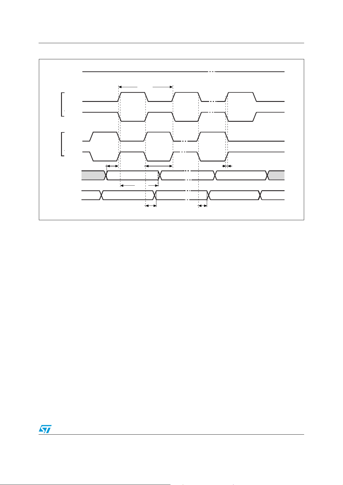
STM32F103xF, STM32F103xG Electrical characteristics
ai14136
SCK Input
CPHA=0
MOSI
OUTUT
MISO
INP UT
CPHA=0
MSBIN
M SB OUT
BIT6 IN
LSB OUT
LSB IN
CPOL=0
CPOL=1
B I T1 OUT
NSS input
t
c(SCK)
t
w(SCKH)
t
w(SCKL)
t
r(SCK)
t
f(SCK)
t
h(MI)
High
SCK Input
CPHA=1
CPHA=1
CPOL=0
CPOL=1
t
su(MI)
t
v(MO)
t
h(MO)
Figure 49. SPI timing diagram - master mode
(1)
1. Measurement points are done at CMOS levels: 0.3V
and 0.7V
DD
DD
.
Doc ID 16554 Rev 3 95/120

Electrical characteristics STM32F103xF, STM32F103xG
Table 57. I2S characteristics
Symbol Parameter Conditions Min Max Unit
DuCy(SCK) I2S slave input clock duty cycle Slave mode 30 70 %
f
CK
1/t
c(CK)
t
r(CK)
t
f(CK)
(1)
t
v(WS)
(1)
t
h(WS)
(1)
t
su(WS)
(1)
t
h(WS)
t
w(CKH)
(1)
t
w(CKL)
t
su(SD_MR)
t
su(SD_SR)
t
h(SD_MR)
t
h(SD_SR)
t
v(SD_ST)
(1)
Master mode (data: 16 bits,
I2S clock frequency
Audio frequency = 48 kHz)
Slave mode 0 6.5
I2S clock rise and fall time Capacitive load CL = 50 pF - 8
WS valid time Master mode 3 -
I2S2 2 -
WS hold time Master mode
I2S3 0 -
WS setup time Slave mode 4 -
WS hold time Slave mode 0 -
CK high and low time
(1)
Data input setup time Master receiver
Master f
frequency = 48 kHz
= 16 MHz, audio
PCLK
I2S2 2 -
I2S3 6.5 -
(1)
Data input setup time Slave receiver 1.5 -
(1)(2)
Data input hold time
(1)(2)
(1)(2)
Data output valid time
Master receiver 0 -
Slave receiver 0.5 -
Slave transmitter (after enable
edge)
1.522 1.525
312.5 -
345 -
- 18
MHz
ns
t
h(SD_ST)
t
v(SD_MT)
t
h(SD_MT)
(1)
Data output hold time
(1)(2)
Data output valid time
(1)
Data output hold time
Slave transmitter (after enable
edge)
Master transmitter (after enable
edge)
Master transmitter (after enable
edge)
1. Based on design simulation and/or characterization results, not tested in production.
2. Depends on f
. For example, if f
PCLK
=8 MHz, then T
PCLK
PCLK
= 1/f
PLCLK
11 -
- 3
0-
=125 ns.
96/120 Doc ID 16554 Rev 3

STM32F103xF, STM32F103xG Electrical characteristics
CK Input
CPOL = 0
CPOL = 1
t
c(CK)
WS input
SD
transmit
SD
receive
t
w(CKH)
t
w(CKL)
t
su(WS)
t
v(SD_ST)
t
h(SD_ST)
t
h(WS)
t
su(SD_SR)
t
h(SD_SR)
MSB receive Bitn receive LSB receive
MSB transmit Bitn transmit LSB transmit
ai14881b
LSB receive
(2)
LSB transmit
(2)
CK output
CPOL = 0
CPOL = 1
t
c(CK)
WS output
SD
receive
SD
transmit
t
w(CKH)
t
w(CKL)
t
su(SD_MR)
t
v(SD_MT)
t
h(SD_MT)
t
h(WS)
t
h(SD_MR)
MSB receive Bitn receive LSB receive
MSB transmit Bitn transmit LSB transmit
ai14884b
t
f(CK)
t
r(CK)
t
v(WS)
LSB receive
(2)
LSB transmit
(2)
(1)
Figure 50. I2S slave timing diagram (Philips protocol)
1. Measurement points are done at CMOS levels: 0.3 × VDD and 0.7 × VDD.
2. LSB transmit/receive of the previously transmitted byte. No LSB transmit/receive is sent before the first
byte.
Figure 51. I2S master timing diagram (Philips protocol)
1. Based on characterization, not tested in production.
2. LSB transmit/receive of the previously transmitted byte. No LSB transmit/receive is sent before the first
byte.
Doc ID 16554 Rev 3 97/120
(1)

Electrical characteristics STM32F103xF, STM32F103xG
t
W(CKH)
CK
D, CMD
(output)
D, CMD
(input)
t
C
t
W(CKL)
t
OV
t
OH
t
ISU
t
IH
t
f
t
r
ai14887
CK
D, CMD
(output)
t
OVD
t
OHD
ai14888
SD/SDIO MMC card host interface (SDIO) characteristics
Unless otherwise specified, the parameters given in Ta bl e 58 are derived from tests
performed under ambient temperature, f
summarized in
Ta bl e 10.
Refer to Section 5.3.14: I/O port characteristics for more details on the input/output alternate
function characteristics (D[7:0], CMD, CK).
Figure 52. SDIO high-speed mode
frequency and VDD supply voltage conditions
PCLKx
Figure 53. SD default mode
98/120 Doc ID 16554 Rev 3

STM32F103xF, STM32F103xG Electrical characteristics
Table 58. SD / MMC characteristics
Symbol Parameter Conditions Min Max Unit
f
PP
t
W(CKL)
t
W(CKH)
t
t
Clock frequency in data transfer
mode
≤ 30 pF 0 48 MHz
C
L
Clock low time, fPP = 16 MHz CL ≤ 30 pF 32 -
Clock high time, fPP = 16 MHz CL ≤ 30 pF 30 -
Clock rise time CL ≤ 30 pF - 4
r
Clock fall time CL ≤ 30 pF - 5
f
CMD, D inputs (referenced to CK)
t
ISU
t
IH
Input setup time CL ≤ 30 pF 2 -
Input hold time CL ≤ 30 pF 0 -
CMD, D outputs (referenced to CK) in MMC and SD HS mode
t
OV
t
OH
CMD, D outputs (referenced to CK) in SD default mode
t
OVD
t
OHD
1. Refer to SDIO_CLKCR, the SDI clock control register to control the CK output.
Output valid time CL ≤ 30 pF - 6
Output hold time CL ≤ 30 pF 0 -
(1)
Output valid default time CL ≤ 30 pF - 7
Output hold default time CL ≤ 30 pF 0.5 -
ns
ns
ns
ns
USB characteristics
The USB interface is USB-IF certified (Full Speed).
Table 59. USB startup time
Symbol Parameter Max Unit
t
STARTUP
1. Guaranteed by design, not tested in production.
(1)
USB transceiver startup time 1 µs
Doc ID 16554 Rev 3 99/120

Electrical characteristics STM32F103xF, STM32F103xG
ai14137
t
f
Differen tial
data lines
V
SS
V
CR S
t
r
Crossover
points
Table 60. USB DC electrical characteristics
Symbol Parameter Conditions Min.
(1)
Input levels
V
V
DI
CM
V
SE
USB operating voltage
DD
(4)
Differential input sensitivity I(USBDP, USBDM) 0.2
(4)
Differential common mode range Includes V
(4)
Single ended receiver threshold 1.3 2.0
(2)
range 0.8 2.5
DI
3.0
(3)
Output levels
SS
(5)
(5)
2.8 3.6
V
V
Static output level low RL of 1.5 kΩ to 3.6 V
OL
Static output level high RL of 15 kΩ to V
OH
1. All the voltages are measured from the local ground potential.
2. To be compliant with the USB 2.0 full-speed electrical specification, the USBDP (D+) pin should be pulled
up with a 1.5 kΩ resistor to a 3.0-to-3.6 V voltage range.
3. The STM32F103xx USB functionality is ensured down to 2.7 V but not the full USB electrical
characteristics which are degraded in the 2.7-to-3.0 V VDD voltage range.
4. Guaranteed by characterization, not tested in production.
is the load connected on the USB drivers
R
5.
L
(1)
Max.
3.6 V
0.3
Unit
VV
V
Figure 54. USB timings: definition of data signal rise and fall time
Table 61. USB: full-speed electrical characteristics
Driver characteristics
Symbol Parameter Conditions Min Max Unit
(2)
(2)
V
t
t
rfm
CRS
Rise time
r
Fall Time
t
f
Rise/ fall time matching tr/t
Output signal crossover voltage 1.3 2.0 V
1. Guaranteed by design, not tested in production.
Measured from 10% to 90% of the data signal. For more detailed informations, please refer to USB
2.
Specification - Chapter 7 (version 2.0).
5.3.18 CAN (controller area network) interface
(1)
CL = 50 pF
420ns
CL = 50 pF 4 20 ns
f
90 110 %
Refer to Section 5.3.14: I/O port characteristics for more details on the input/output alternate
function characteristics (CAN_TX and CAN_RX).
100/120 Doc ID 16554 Rev 3
 Loading...