

ST STHDLS101T User Manual
Features
■ Converts low-swing alternating current (AC)
coupled differential input to high-definition
multimedia interface (HDMI) rev 1.3 compliant
■ HDMI level shifting operation up to 2.7 Gbps
per lane
■ Integrated 50-Ω termination resistors for AC-
coupled differential inputs
■ Input/output transition minimized differential
signaling (TMDS) enable/disable
■ Output slew rate control on TMDS outputs to
minimize electromagnetic interference (EMI)
■ Fail safe outputs for backdrive protection
■ No re-timing or configuration required
■ Inter-pair output skew < 250 ps
■ Intra-pair output skew < 10 ps
■ Single power supply of 3.3 V
■ ESD protection: ±6 KV HBM on all I/O pins
■ Integrated display data channel (DDC) level
shifters. Pass-gate voltage limiters allow 3.3 V
termination on graphics and memory controller
hub (GMCH) pins and 5 V DDC termination on
HDMI connector pins
■ Level shifter and configurable output for HPD
signal from HDMI/DVI connector
■ Integrated pull-down resistor on HPD_SINK
and OE_N inputs
Applications
■ Notebooks
■ PC motherboards and graphic cards
■ Dongles/cable adapters
Table 1. Device summary
STHDLS101T
AC coupled HDMI level shifter
with configurable HPD output
QFN-48
(7 x 7 mm)
Description
The STHDLS101T is a high-speed high-definition
multimedia interface (HDMI) level shifter that
converts low-swing AC coupled differential input
to HDMI 1.3 compliant open-drain current
steering RX-terminated differential output.
Through the existing PCI-E pins in the graphics
and memory controller hub (GMCH) of PCs or
notebook motherboards, the pixel clock provides
the required bandwidth (1.65 Gbps, 2.25 Gbps)
for the video supporting 720p, 1080i, 1080p with a
total of 36-bit resolution. The HDMI is multiplexed
onto the PCIe pins in the motherboard where the
AC coupled HDMI at 1.2 V is output by GMCH.
The AC coupled HDMI is then level shifter by this
device to 3.3 V DC coupled HDMI output.
The STHDLS101T supports up to 2.7 Gbps,
which is enough for 12-bits of color depth per
channel, as indicated in HDMI rev 1.3. The device
operates from a single 3.3 V supply and is
available in a 48-pin QFN package.
Order code Package Packaging
STHDLS101TQTR QFN-48 Tape and reel
December 2008 Rev 3 1/26
www.st.com
26

Contents STHDLS101T
Contents
1 Block diagram . . . . . . . . . . . . . . . . . . . . . . . . . . . . . . . . . . . . . . . . . . . . . . 3
2 System interface . . . . . . . . . . . . . . . . . . . . . . . . . . . . . . . . . . . . . . . . . . . . 4
3 Pin configuration . . . . . . . . . . . . . . . . . . . . . . . . . . . . . . . . . . . . . . . . . . . . 6
3.1 Pin description . . . . . . . . . . . . . . . . . . . . . . . . . . . . . . . . . . . . . . . . . . . . . . 7
4 Functional description . . . . . . . . . . . . . . . . . . . . . . . . . . . . . . . . . . . . . . 11
5 Maximum ratings . . . . . . . . . . . . . . . . . . . . . . . . . . . . . . . . . . . . . . . . . . . 13
5.1 Recommended operating conditions . . . . . . . . . . . . . . . . . . . . . . . . . . . . 14
5.1.1 Power supply and temperature range . . . . . . . . . . . . . . . . . . . . . . . . . . 14
5.1.2 Differential inputs (IN_D signals) . . . . . . . . . . . . . . . . . . . . . . . . . . . . . . 14
5.2 TMDS outputs (OUT_D signals) . . . . . . . . . . . . . . . . . . . . . . . . . . . . . . . . 15
5.3 HPD input and output characteristics . . . . . . . . . . . . . . . . . . . . . . . . . . . . 16
5.4 DDC input and output chatacteristics . . . . . . . . . . . . . . . . . . . . . . . . . . . . 17
5.5 OE_ input characteristics . . . . . . . . . . . . . . . . . . . . . . . . . . . . . . . . . . . . . 18
5.6 HPD input resistor . . . . . . . . . . . . . . . . . . . . . . . . . . . . . . . . . . . . . . . . . . 18
5.7 ESD performance . . . . . . . . . . . . . . . . . . . . . . . . . . . . . . . . . . . . . . . . . . . 18
6 Application information . . . . . . . . . . . . . . . . . . . . . . . . . . . . . . . . . . . . . 19
6.1 Power supply sequencing . . . . . . . . . . . . . . . . . . . . . . . . . . . . . . . . . . . . . 19
6.2 Supply bypassing . . . . . . . . . . . . . . . . . . . . . . . . . . . . . . . . . . . . . . . . . . . 19
6.3 Differential traces . . . . . . . . . . . . . . . . . . . . . . . . . . . . . . . . . . . . . . . . . . . 19
7 Package mechanical data . . . . . . . . . . . . . . . . . . . . . . . . . . . . . . . . . . . . 20
8 Revision history . . . . . . . . . . . . . . . . . . . . . . . . . . . . . . . . . . . . . . . . . . . 24
2/26

STHDLS101T Contents
3/26
Block diagram STHDLS101T
1 Block diagram
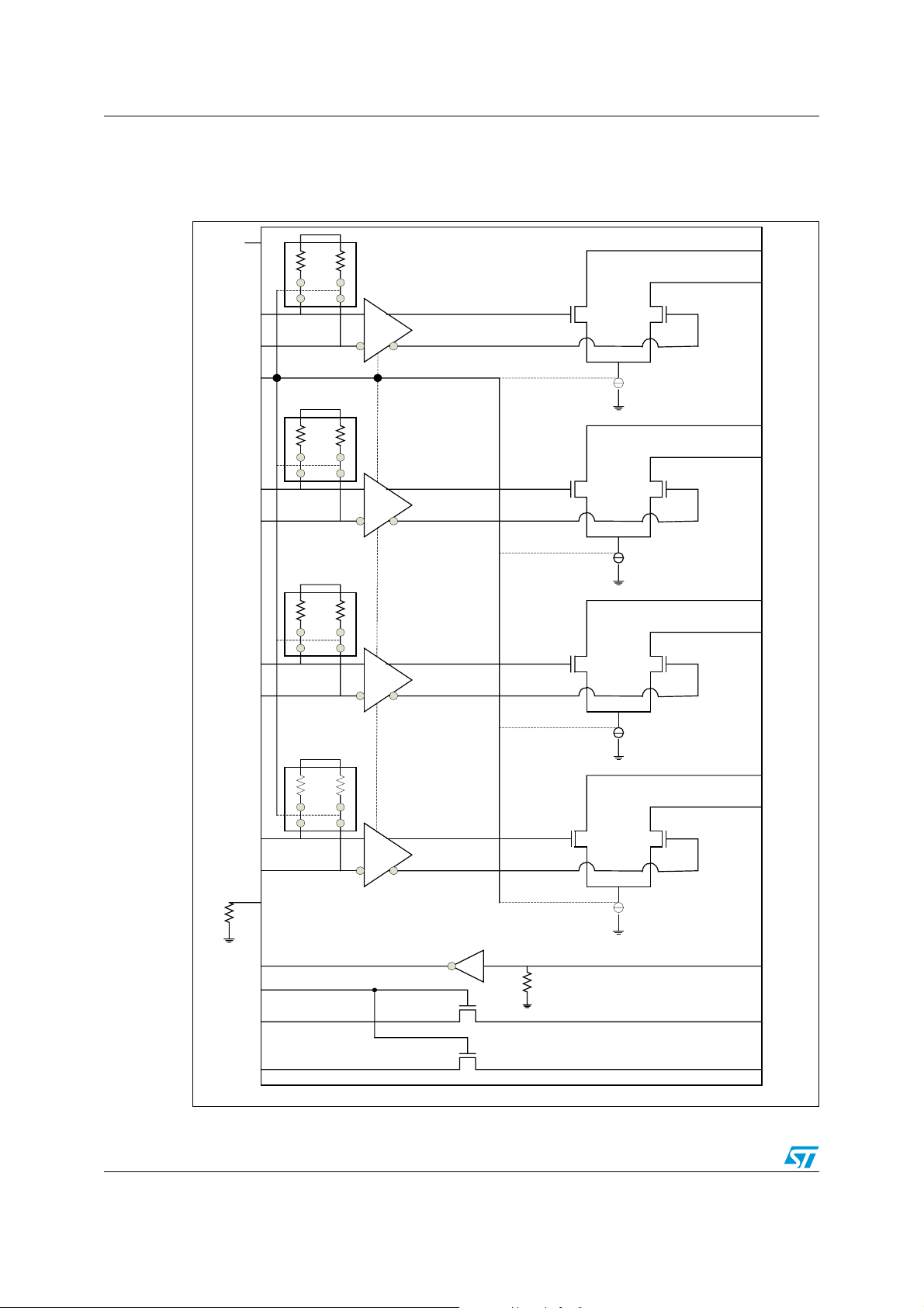
Figure 1. STHDLS101T block diagram
0
VCC33
IN_D4+
IN_D4-
V
50 ±10%
Ω
OUT_D4+
OUT_D4-
RX
OE_N
IN_D3+
IN_D3-
IN_D2+
IN_D2-
0V
Ω
50 ±10%
0V
50 ±10%
Ω
0V
50
Ω±10%
10mA current
driver
OUT_D3+
OUT_D3-
RX
10mA current
driver
OUT_D2+
OUT_D2-
RX
10mA current
driver
OUT_D1+
OUT_D1-
4/26
IN_D1+
RX
IN_D1-
REXT
HPD level
shifter
HPD_SOURCE HPD_SINK
DDC_EN
SCL_SOURCE
SDA_SOURCE
HPD
160
K
10mA current
driver
SCL_SINK
SDA_SINK
STHDLS101T System interface
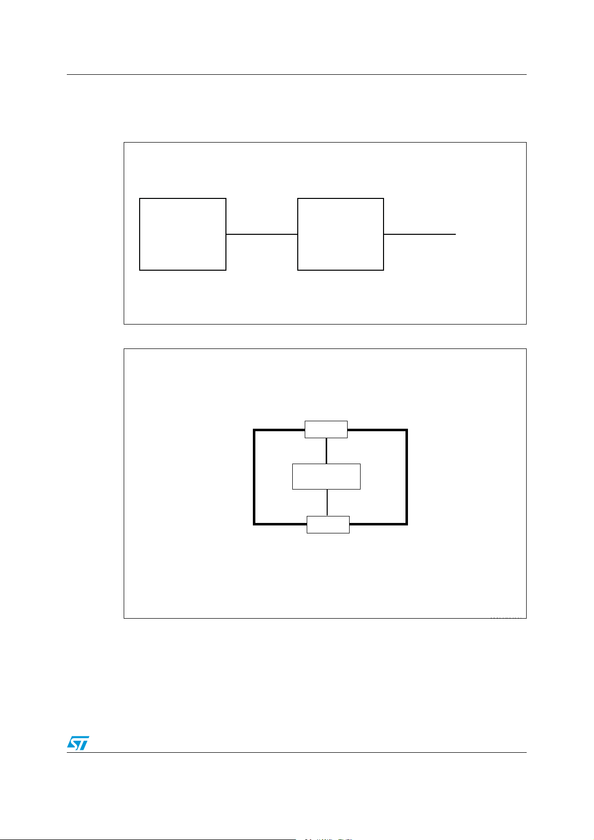
2 System interface
Figure 2. System inferface
PCI-Express
SDVO
Graphics chipset
(GMCH) on the
motherboard
Figure 3. Cable adapter
HDMI
Level shifter
STHDLS101T
HDMI output
connector
CS00375
$ONGLEOR
ADAPTER
CABLE
($-)$6)
34($,3
$0
4
5/26
System interface STHDLS101T
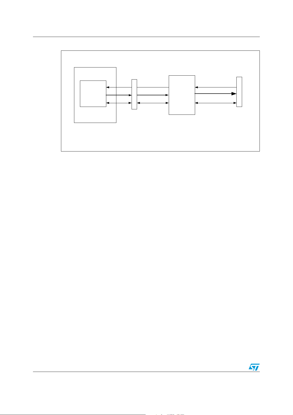
Figure 4. DP to HDMI/DVI cable adapter
HDMI/DVI
Transmitter
PC chipset
HPD
AC_TMDS
DDC
HPD_SOURCE
DP Connector
AC_TMDS
DDC
STHDLS101T
HDMI/DVI Cable
Adaptor
HPD_SINK
DC TMDS
DDC
HDMI/DVI Connector
!-6
6/26
STHDLS101T Pin configuration
3 Pin configuration
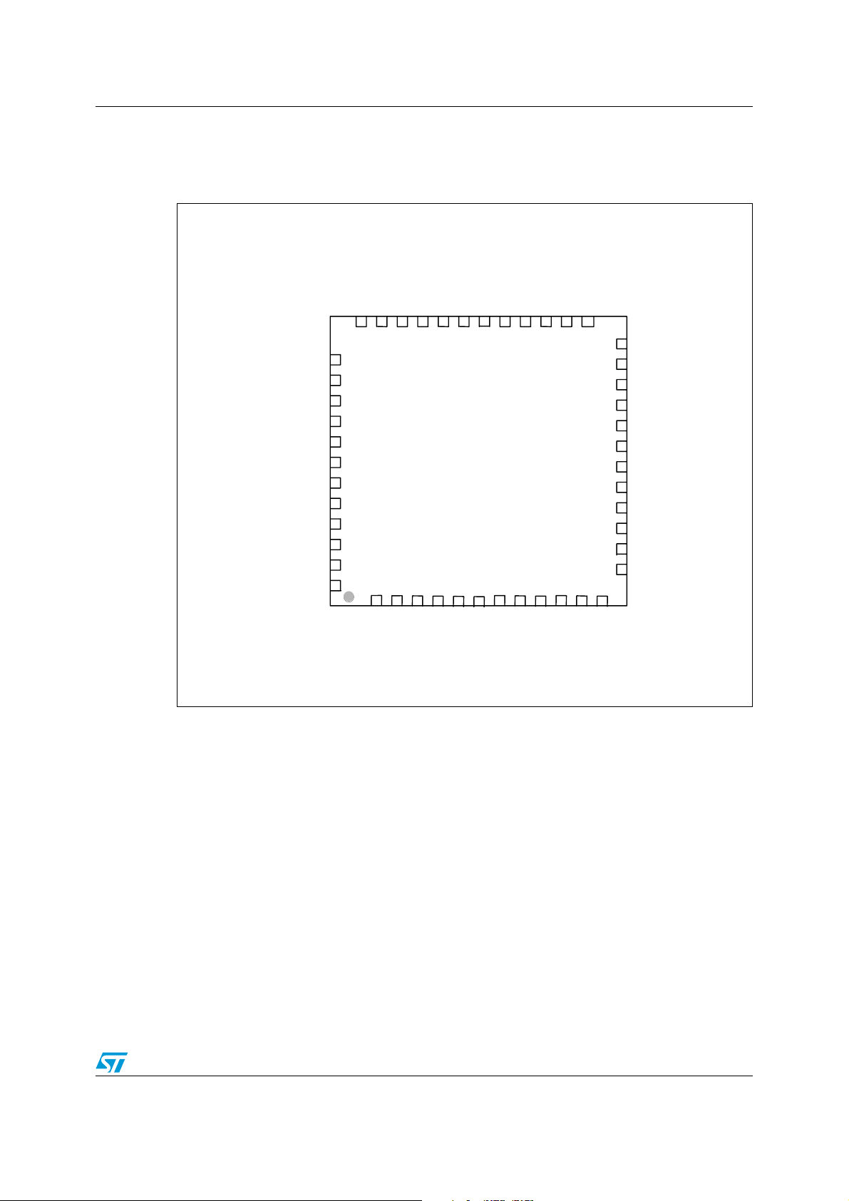
Figure 5. STHDLS101T pin configuration
FUNCTION4
GND
FUNCTION3
VCC33
DDC_EN
GND
HPD_SINK
SDA_SINK
SCL_SINK
GND
VCC33
OE_N
GND
IN_D1-
IN_D1+
VCC33
IN_D2-
IN_D2+
GND
IN_D3-
IN_D3+
VCC33
IN_D4-
IN_D4+
31
33
35
1
GND
34
2
33
VCC
4
3
FUNCTION1
FUNCTION2
36
37
38
39
40
41
42
43
44
45
46
47
48
32
QFN-48
5
6
GND
REXT
30
29
7
8
SOURCE
SDA_
HPD_SOURCE
27
28
9
RCE
SOU
SCL_
24
26
25
23
22
21
20
19
18
17
16
15
14
13
10
11
33
VCC
ANALOG2
GND
OUT_D1-
OUT_D1+
VCC33
OUT_D2-
OUT_D2+
GND
OUT_D3-
OUT_D3+
VCC33
OUT_D4-
OUT_D4+
12
GND
CS000118
7/26
Pin configuration STHDLS101T
3.1 Pin description
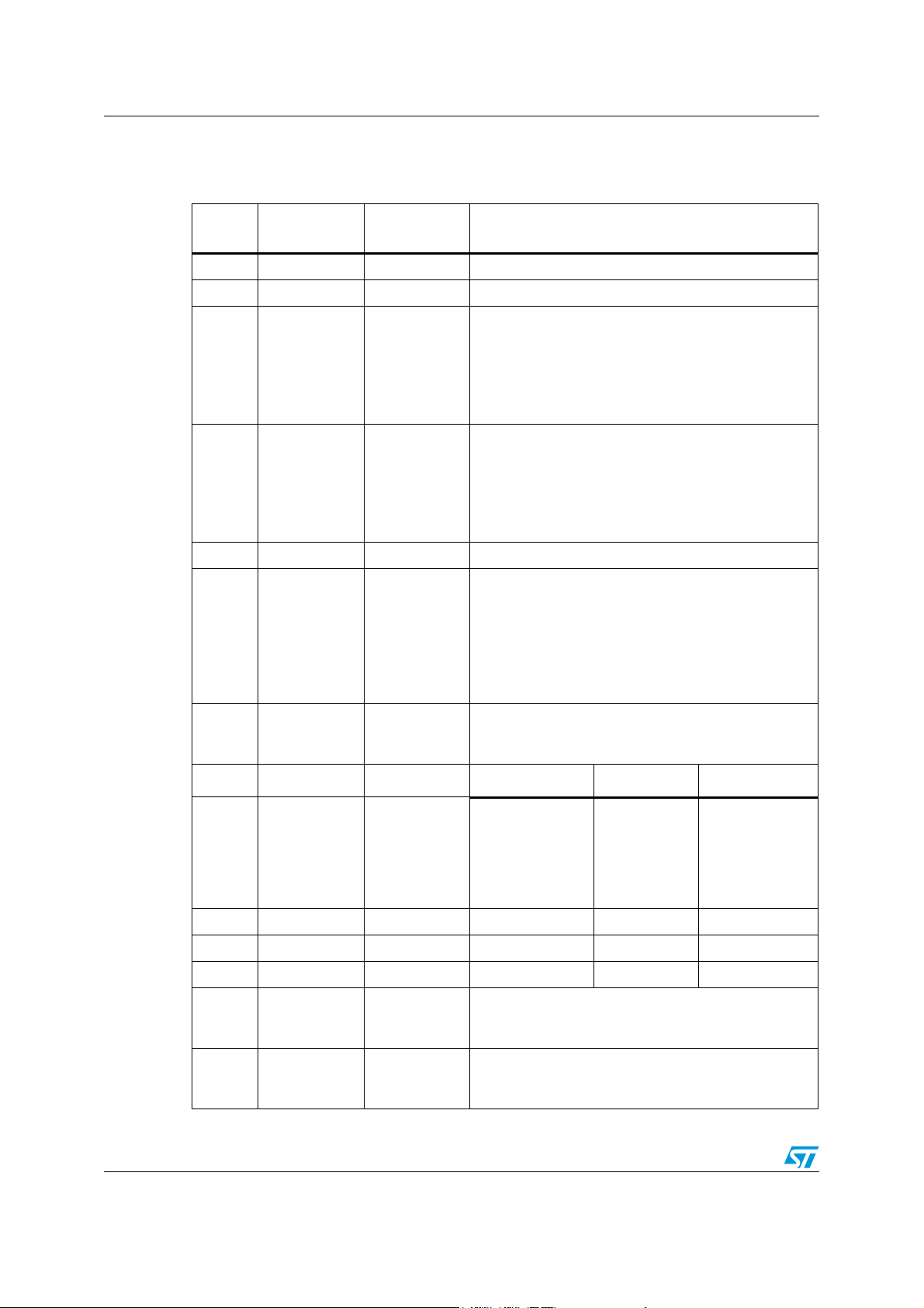
Table 2. Pin description
Pin
number
1GND PowerGround
2 VCC33 Power 3.3V±10% DC supply
3 FUNCTION1
4 FUNCTION2
5GND PowerGround
6 REXT Analog
7 HPD_SOURCE Output
Name Type Function
Function pins are to enable vendor-specific features or
Vendor-specific
control or test
pins
Vendor-specific
control or test
pins
test modes.
For normal operation, these pins are tied to GND or
VCC33.
For consistent interoperability, GND is the preferred
default connection for these signals
Function pins are to enable vendor-specific features or
test modes.
For normal operation, these pins are tied to GND or
VCC33.
For consistent interoperability, GND is the preferred
default connection for these signals
Connection to external resistor. Resistor value
specified by device manufacturer.
Acceptable connections to this pin are:
- Resistor to GND
- Resistor to 3.3V;
- NC (direct connections to V
0-Ù resistor for layout compatibility
Buffer from the 0 V to 5 V input signal. The output
buffer stage is configurable based on the FUNCTION3
pin settings as desribed in the table below:
or GND are through a
CC
8/26
8 SDA_SOURCE I/O
9 SCL_SOURCE Input
FUNCTION3 HPD_SINK HPD_SOURCE
Open-drain,
connected an
0Low
0 High (5 V) Low (0 V)
1 Low (0 V) Low (0 V)
1 High (5 V) High (3 V)
3.3 V DDC data I/O. Pulled-up by external termination
to 3.3 V. Connected to SDA_SINK through voltagelimiting integrated NMOS pass-gate
3.3 V DDC clock I/O. Pulled-up by external termination
to 3.3 V. Connected to SCL_SINK through voltagelimiting integrated NMOS pass-gate
external pull up to
the desired
supply
(normally 1 V)
 Loading...