

1
3
查询STGW30NC60W供应商
STGW30NC60W
N-CHANNEL 30A - 600V - TO-247
Ultra FAST Switching PowerMESH™ IGBT
Target Specification
General features
V
Type
STGW30NC60W 600 V < 2.5 V 30 A
■ VERY LOW OFF LOSSES INCLUDING TAIL
V
CES
CE(sat)
(Max )@ 25°C
CURRENT
■ LOWER C
■ LOSSES INCLUDE DIODE RECOVERY
RES
/ C
IES
RATIO
ENERGY
■ HIGH FREQUENCY OPERATION
■ VERY SOFT ULTRA FAST RECO VERY ANTI
PARALLEL DIODE
I
C
@100°C
Description
Using the latest high voltage technology based on
a patented strip layout, STMicroelectronics has
designed an advanced family of IGBTs, the
PowerMESH
performances. The suffix “W” identifies a family
optimized for very high frequency application.
™
IGBTs, with outstanding
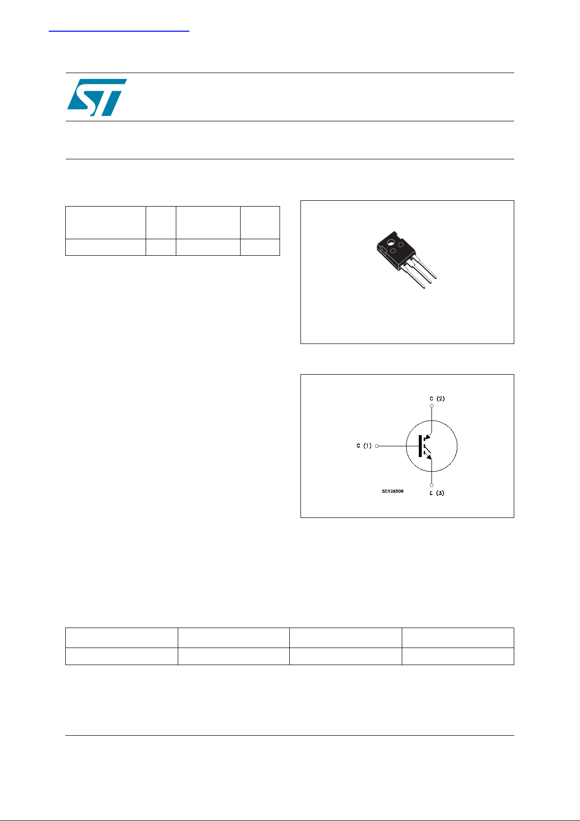
Package
2
TO-247
Internal schematic diagram
Applications
■ HIGH FREQUENCY INVERTERS, UPS,
MOTOR DRIVERS
■ HF, SMPS and PFC IN BOTH HARD SWITCH
AND RESONANT TOPOLOGIES
Order codes
Sales Type Marking Package Packaging
STGW30NC60W W30NC60W TO-247 TUBE
Rev 1
September 2005 1/9
www.st.com
9This is a preliminary information on a new product foreseen to be developed. Details are subject to change without notice
1 Electrical ratings STGW30NC60W
1 Electrical ratings
Table 1. Absolute maximum ratings
Symbol Parameter Value Unit
V
CES
I
C
I
C
V
ECR
V
GE
ICM Note 1
P
TOT
Collector-Emitter Voltage (VGS = 0)
600 V
Collector Current (cont inuous) at 25°C (#) 60 A
Collector Current (continuous) at 100°C (#) 30 A
Reverse Battery Protect ion 20 V
Gate-Emitter Voltage ± 20 V
Collector Current (pulsed) 100 A
Total Dissipat ion at TC = 25°C
200 W
Derating Factor 1.6 W/°C
T
stg
T
Table 2. Thermal Data
Storage Tem perature
Operating Junction Tem perature
j
– 55 to 150 °C
Min. Typ. Max. Unit
Rthj-case Thermal Resist ance Junction-case 0.625 °C/W
Rthj-amb Thermal Resist ance Junction-ambient 62.5 ° C/W
T
L
Maximum Lead Tempe ratur e for Solder ing Pu rpo se
(1.6 mm from case, for 10 sec.)
300
°C
2/9
STGW30NC60W 2 Electrical characteristics
2 Electrical characteristics
(T
= 25 °C unless otherwise specified)
CASE
Table 3. Static
Symbol Parameter T est Conditions Min. Typ. Max. Unit
V
BR(CES)
V
CE(SAT)
Collectro-Emitter Breakdown
Voltage
Colle ct o r-Emitte r S at u ra ti o n
Voltage
I
= 1 mA, VGE = 0
C
V
= 15 V, IC= 20A, Tj= 25°C
GE
V
= 15 V, IC= 20A,
GE
600 V
1.9
1.8
2.5
Tj= 125°C
= VGE, IC= 250 µA
V
g
fs
GE(th)
I
CES
I
GES
Note 1
Gate Threshold Voltage
Collector-Emitter Leakage
Current (V
CE
= 0)
Gate-Emitter Leak age
Current (V
CE
= 0)
Forward Transconductance
V
CE
V
= Max Rating,Tc=25°C
GE
V
= Max Rating, Tc=125°C
GE
= ± 20 V , VCE = 0
V
GE
VCE = 15 V, IC= 20 A
3.75 5.75 V
10
1
± 10 0 nA
15 S
Table 4. Dynamic
Symbol Parameter Test Conditions Min. Typ. Max. Unit
C
ies
C
oes
C
res
Input Capacitan ce
Output Capacitance
Reverse Transfer Capacitance
= 25V, f = 1 MHz, VGE =
V
CE
0
2200
225
50
V
V
µA
mA
pF
pF
pF
Q
g
Q
ge
Q
gc
I
CL
Total Gate Charge
Gate-Emitter Charge
Gate-Collecto r Char ge
Turn-Off SOA Minimum
Current
= 390 V, IC = 20 A,
V
CE
V
= 15V,
GE
(see Figure 2)
V
= 480 V , Tj = 150°C
clamp
R
= 10 Ω, VGE= 15V
G
100
16
45
140 nC
nC
nC
100 A
3/9

2 Electric al characteristics STGW30NC60W
Table 5. Switching On/Off
Symbol Parameter Test Conditions Min. Typ. Max. Unit
t
d(on)
t
(di/dt)
t
d(on)
t
(di/dt)
t
r(Voff
t
d(off
t
t
r(Voff
t
d(off
t
Turn-on Delay Time
r
Current Rise Time
Turn-on Curr ent Slope
on
Turn-on Delay Time
r
f
f
Current Rise Time
Turn-on Curr ent Slope
on
)
Off Voltage Rise Time
)
Turn-off De la y Tim e
Cur r e n t Fa ll Time
)
Off Voltage Rise Time
)
Turn-off De la y Tim e
Cur r e n t Fa ll Time
= 390 V, IC = 20 A
V
CC
= 10 Ω, VGE= 15V, Tj= 25°C
R
G
(see Figure 3)
= 390 V, IC = 20 A
V
CC
= 10 Ω, VGE= 15V, Tj= 125°C
R
G
(see Figure 3)
= 390 V, IC = 5 A,
V
cc
= 10 Ω , VGE = 15 V, TJ=25°C
R
GE
(see Figure 3)
= 390 V, IC = 5 A,
V
cc
=10 Ω , VGE =15 V, Tj=125 °C
R
GE
(see Figure 3)
31
11
1600
31
11.5
1500
16.5
115
38
34
152
48
Table 6. Switching energy
Symbol Parameter T est Conditions Min. Typ. Max. Unit
Note 3
Eon
E
off
Eon
E
off
Note 4
E
ts
Note 3
Note 4
E
ts
Turn-on Switching Losses
Turn-off Switching Losses
Total Swit chin g Lo s s es
Turn-on Switching Losses
Turn-off Switching Losses
Total Swit chin g Lo s s es
= 390 V, IC = 75 A
V
CC
R
= 10 Ω, VGE= 15V, Tj= 25°C
G
(see Figure 3)
= 390 V, IC = 5 A
V
CC
R
= 10 Ω, VGE= 15V, Tj= 125°C
G
(see Figure 3)
200
205
405
400
365
765
ns
ns
A/µs
ns
ns
A/µs
ns
ns
ns
ns
ns
ns
µJ
µJ
µJ
µJ
µJ
µJ
(1)Pu ls e w id th lim ited by max. junction te m pe rature
(2) Eon is the tun-on losses when a typical diode is used in the test circuit in figure 2. If the IGBT is offered in a package with a
co-pak diode, the co-pack diode is used as external diode. IGBTs & Diode are at the same temperature (25°C and 125°C)
(3) Turn-off losses include also the tail of the collector current
4/9

STGW30NC60W 3 Test Circuits
3 Test Circuits
Figure 1. Test Circuit for Inductive Load
Switching
Figure 3. Switching Waveform
Figure 2. Gate Charge Test Circuit
5/9

4 Package mechani cal data STGW30NC60W
4 Package m echanical data
In order to meet environmental requirements, ST offers these devices in ECOPACK®
packages. These packages have a Lead-free second level interconnect . The category of
second level interconnect is marked on the package and on the inner box label, in compliance
with JEDEC Standard JESD97. The maximum ratings related to soldering conditions are also
marked on the inner box label. ECOP ACK is an ST trademark. ECOPACK specifications are
available at: www.st.com
6/9

STGW30NC60W 4 Package mechanical data
TO-247 MECHANICAL DATA
DIM.
A 4.85 5.15 0.19 0.20
A1 2.20 2.60 0.086 0.102
b 1.0 1.40 0.039 0.055
b1 2.0 2.40 0.079 0.094
b2 3.0 3.40 0.118 0.134
c 0.40 0.80 0.015 0.03
D 19.85 20.15 0.781 0.793
E 15.45 15.75 0.608 0.620
e5.45 0.214
L 14.20 14.80 0.560 0.582
L1 3.70 4.30 0.14 0.17
L2 18.50 0.728
øP 3.55 3.65 0.140 0.143
øR 4.50 5.50 0.177 0.216
S5.50 0.216
MIN. TYP MAX. MIN. TYP. MAX.
mm. inch
7/9

5 Revision Hist ory STGW30NC60W
5 Revision History
Date Revision Changes
15-Sep-2005 1 Initial release.
8/9

STGW30NC60W 5 Revision History
I
s
o
d
b
ct
t
ot
a
nformation furnished is believed to be accurate and reliable. However, STMicroelectronics assumes no responsibility for the consequence
f use of such information nor for any infringement of patents or other rights of third parties which may result from its use. No license is grante
y implic ation or oth erwise unde r any paten t or patent ri ghts of STMi croelectronics. Spec i fications mentioned in this publ ic at i on are sub je
o change without notice. This publication supersedes and replaces all information previously supplied. STMicroelectronics products are n
uthoriz ed for use as crit ical component s i n l i fe support devices or systems wi thout express written appr oval of STMicroelectronics.
The ST logo is a registered trademark of STM i croelectroni cs.
All other nam es are the property of their respective owners
© 2005 STMi croelectro ni cs - All rights reserved
Austra l i a - Be l gi um - Brazil - C anada - China - Czech Republic - Finland - France - Germany - Hong Kong - In di a - Israel - Ital y - Japan -
Malaysi a - M al ta - Morocco - Singapore - Sp ai n - S weden - Swit zerland - Uni ted Kingdom - United States of America
STMicroelectronics group of companies
www.st.com
9/9
 Loading...