

STGP14NC60KD - STGF14NC60KD
1
3
1
3
3
STGB14NC60KD
N-CHANNEL 14A - 600V - TO-220/TO-220FP/D2PAK
SHORT CIRCUIT RATED PowerMESH™ IGBT
Table 1: General Feature s
TYPE V
STGB14NC60KD
STGF14NC60KD
STGP14NC60KD
■ LOWER ON-VOLTAGE DROP (V
■ OFF LOSSES INCLUDE TAIL CURRENT
■ LOWER C
■ SWITCHING LOSSES INCLUDE DIODE
RES
CESVCE(sat)
600 V
600 V
600 V
/ C
RATIO
IES
@25°C
< 2.5 V
< 2.5 V
< 2.5 V
(Max)
cesat
IC (#)
@100°C
14 A
7 A
14 A
)
RECOVERY ENERGY
■ VERY SOFT U LTRA F AST REC OVER Y
ANTIPARALLEL DIODE
■ NEW GENERATION PRODUCTS WITH
TIGHTER PARAMETER DISTRUBUTION
DESCRIPTION
Using the latest high voltage technology bas ed on
a patented strip layout, STMicroelectronics has
design ed an adva nced fam ily of IGBT s, the P ow
erMESH™ IGBTs, with outstanding performances.
The suffix “K” identifies a family optimized for high
freque ncy mot or cont rol appl icat ions wi th shor t cir
cuit withstand capability.
APPLICATIONS
■ HIGH FREQUENCY INVERTERS
■ SMPS and PFC IN BOTH HARD SWITCH AND
RESONANT TOPOLOGIES
■ MOTOR DRIVERS
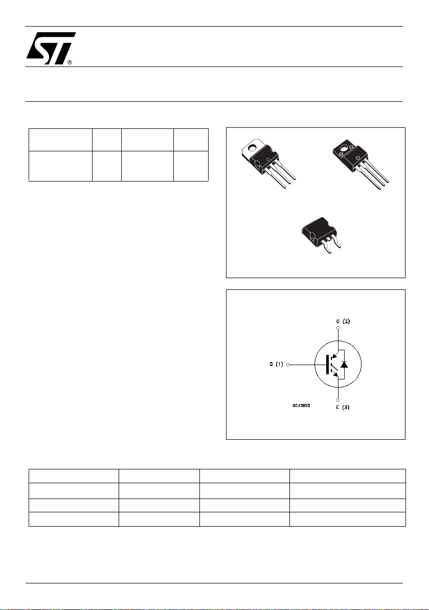
Figure 1: Package
2
TO-220
2
PAK
D
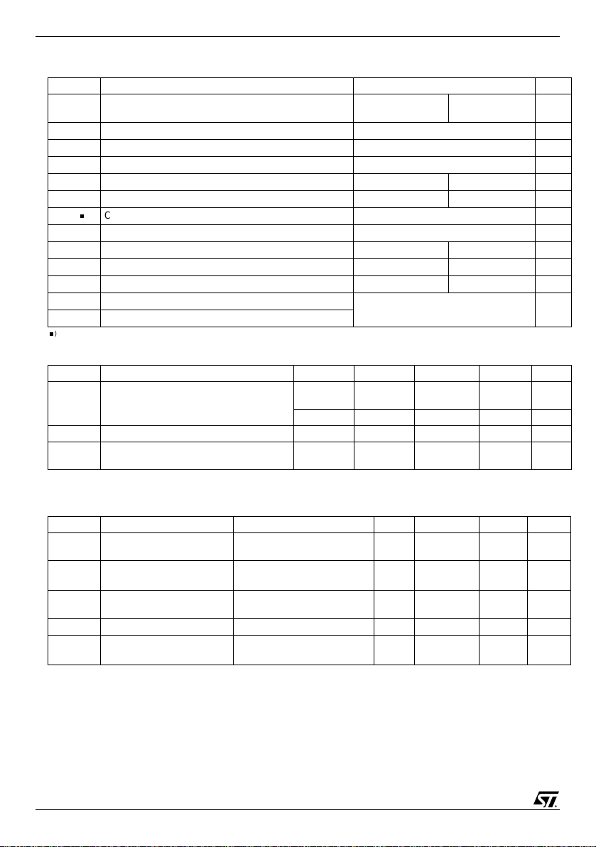
Figure 2: Internal Schematic Diagram
-
-
2
TO-220FP
1
Table 2: Order Codes
SALES TYPE MARKING PACKAGE PACKAGING
STGB14NC60KDT4 GB14NC60KD
STGF14NC60KD GF14NC60KD TO-220FP TUBE
STGP14NC60KD GP14NC60KD TO-220 TUBE
D2PAK
TAPE & REEL
Rev.2
1/14July 2005
STGP14NC60KD - STGF14NC60KD - STGB14NC60KD
Table 3: Abso lute Ma ximu m ratings
Symbol Parameter Value Unit
STGB14NC60KD
STGP14NC60KD
V
Collector-Emitter Voltage (VGS = 0)
CES
V
Emitter-Collector Voltage 20 V
ECR
V
Gate-Emitter Voltage ±20 V
GE
I
Collector Current (continuous) at TC = 25°C (#)
C
I
Collector Current (continuous) at TC = 100°C (#)
C
I
()
Collector Current (pulsed) 50 A
CM
I
Diode RMS Forward Current at TC = 25°C
F
P
Total Dissipation at TC = 25°C
TOT
25 11 A
14 7 A
80 25 W
Derating Factor 0.64 0.20 W/°C
V
Insulation Withstand Voltage A.C.(t = 1 sec; Tc = 25°C) -- 2500 V
ISO
T
Storage Temperature
stg
T
Operating Junction Temperature
j
() Pulse width limited by Max Junction Temperature.
Table 4: Thermal Data
Min. Typ. Max.
Rthj-case Thermal Resistance Junction-case TO-220
D²PAK
TO-220FP 5.0 °C/W
Rthj-amb Thermal Resistance Junction-ambient 62.5 °C/W
T
Maximum Lead Temperature for Soldering
L
Purpose (1.6 mm from case, for 10 sec.)
STGF14NC60KD
600 V
20 A
– 55 to 150 °C
1.56 °C/W
300 °C
ELECTRICAL CHARACTERISTICS (T
=25°C UNLESS OTHERWISE SPECIFIED)
CASE
Table 5: Main Parameters
Symbol Parameter Test Conditions Min. Typ. Max. Unit
V
BR(CES)
V
V
(#) Calculated according to the iterative formula:
ICTC()
2/14
Collector-Emitter
Breakdown Voltage
I
Collector cut-off Current
CES
(VGE = 0)
I
Gate-Emitter Leakage
GES
Current (VCE = 0)
Gate Threshold Voltage
GE(th)
Collector-Emitter Saturation
CE(sat)
Voltage
T
--------------------------------------------------------------------------------------------------
=
R
THJ C–VCESAT MAX()TCIC
JMAXTC
IC= 1 mA, VGE= 0 600 V
VCE= Max Rating, TC= 25°C
VCE= Max Rating, TC= 125°C
10
1
VGE= ±20V , VCE= 0 ±100 nA
VCE= VGE, IC= 250 µA
VGE= 15V, IC= 7A
VGE= 15V, IC= 7A, Tc= 125°C
–
,()×
5 7 V
2.0
1.8
2.5 V
µA
mA
V

STGP14NC60KD - STGF14NC60KD - STGB14NC60KD
ELECTRICAL CHARACTERISTICS (CONTINUED)
Table 6: Dynamic
Symbol Parameter Test Conditions Min. Typ. Max. Unit
gfs (1)
C
C
C
Q
Q
t
Forward Transconductance
Input Capacitance
ies
Output Capacitance 86 pF
oes
Reverse Transfer
res
Capacitance
Q
Total Gate Charge
g
Gate-Emitter Charge
ge
Gate-Collector Charge
gc
Short Circuit Withstand Time VCE = 0.5 V
scw
Table 7: Switching On
Symbol Parameter Test Conditions Min. Typ. Max. Unit
t
d(on)
(di/dt)
t
d(on)
(di/dt)
Turn-on Delay Time
Current Rise Time
t
r
Turn-on Current Slope
on
Turn-on Delay Time
Current Rise Time
t
r
Turn-on Current Slope
on
Table 8: Switching Off
Symbol Parameter Test Conditions Min. Typ. Max. Unit
tr(V
)
Off Voltage Rise Time
off
td(
tr(V
td(
Turn-off Delay Time
)
off
Current Fall Time
t
f
)
Off Voltage Rise Time
off
Turn-off Delay Time
)
off
Current Fall Time
t
f
VCE = 15 V , IC = 7 A 3 S
VCE = 25 V, f= 1 MHz, VGE = 0
760 pF
15.5 pF
VCE = 390 V, IC = 7 A,
VGE = 15 V
(see Figure 21)
RG = 10 Ω, VGE = 12 V
BR(CES),Tj
= 125°C,
VCC = 390 V, IC = 7 A
RG= 10 Ω, VGE= 15V, Tj= 25°C
(see Figure 19)
VCC = 390 V, IC = 7 A
RG= 10 Ω, VGE= 15V, Tj= 125°C
(see Figure 19)
Vcc = 390 V, IC = 7 A,
RGE = 10 Ω , VGE = 15 V
TJ = 25 °C
34.4
8.1
16.4
10 µs
22.5
8.5
700
22
9.5
680
60
116
75
(see Figure 19)
Vcc = 390 V, IC = 7 A,
RGE = 10 Ω , VGE = 15 V
Tj = 125 °C
(see Figure 19)
24
196
144
nC
nC
nC
ns
ns
A/µs
ns
ns
A/µs
ns
ns
ns
ns
ns
ns
Table 9: Switching Energy
Symbol Parameter Test Conditions Min. Typ. Max. Unit
Eon (2)
E
off
E
Eon (2)
E
off
E
(1) Pulsed: Pulse duration = 300 µs, duty cycle 1.5%
(2) Eon is the turn-on l osses when a typical di ode i s used i n the test ci rcuit in fi gure 2. If the IG BT is o ffered in a pac kage with a co -pack diode ,
the co-pack diode is used as external diode. IGBTs & DIODE are at the same temperature (25°C and 125°C)
(3)Turn-off losses include also the tail of the collector current.
Turn-on Switching Losses
Turn-off Switching Losses
(3)
Total Switching Losses
ts
Turn-on Switching Losses
Turn-off Switching Losses
(3)
Total Switching Losses
ts
VCC = 390 V, IC = 7 A
RG= 10 Ω, VGE= 15V, Tj= 25°C
(see Figure 19)
VCC = 390 V, IC = 7 A
RG= 10 Ω, VGE= 15V, Tj= 125°C
(see Figure 19)
82
155
237
131
370
501
µJ
µJ
µJ
µJ
µJ
µJ
3/14
STGP14NC60KD - STGF14NC60KD - STGB14NC60KD
Table 10: Collector-Emitter Diode
Symbol Parameter Test Condiction Min. Typ. Max. Unit
V
Forward O n-Voltage If = 3.5 A
f
If = 3.5 A, Tj = 125 °C
t
Reverse Recovery Time
rr
t
a
Q
I
Q
I
Reverse Recovery Charge
rr
Reverse Recovery Current
rrm
Softness factor of the diode
S
t
Reverse Recovery Time
rr
t
a
Reverse Recovery Charge
rr
Reverse Recovery Current
rrm
Softness factor of the diode
S
If = 7 A, VR = 40 V,
Tj = 25 °C, di/dt = 100 A/µs
0.68
If = 7 A, VR = 40 V,
Tj = 125 °C, di/dt = 100 A/µs
0.79
1.3
1.1
37
22
40
2.1
61
34
98
3.2
1.9
V
V
ns
ns
nC
A
ns
ns
nC
A
4/14
STGP14NC60KD - STGF14NC60KD - STGB14NC60KD
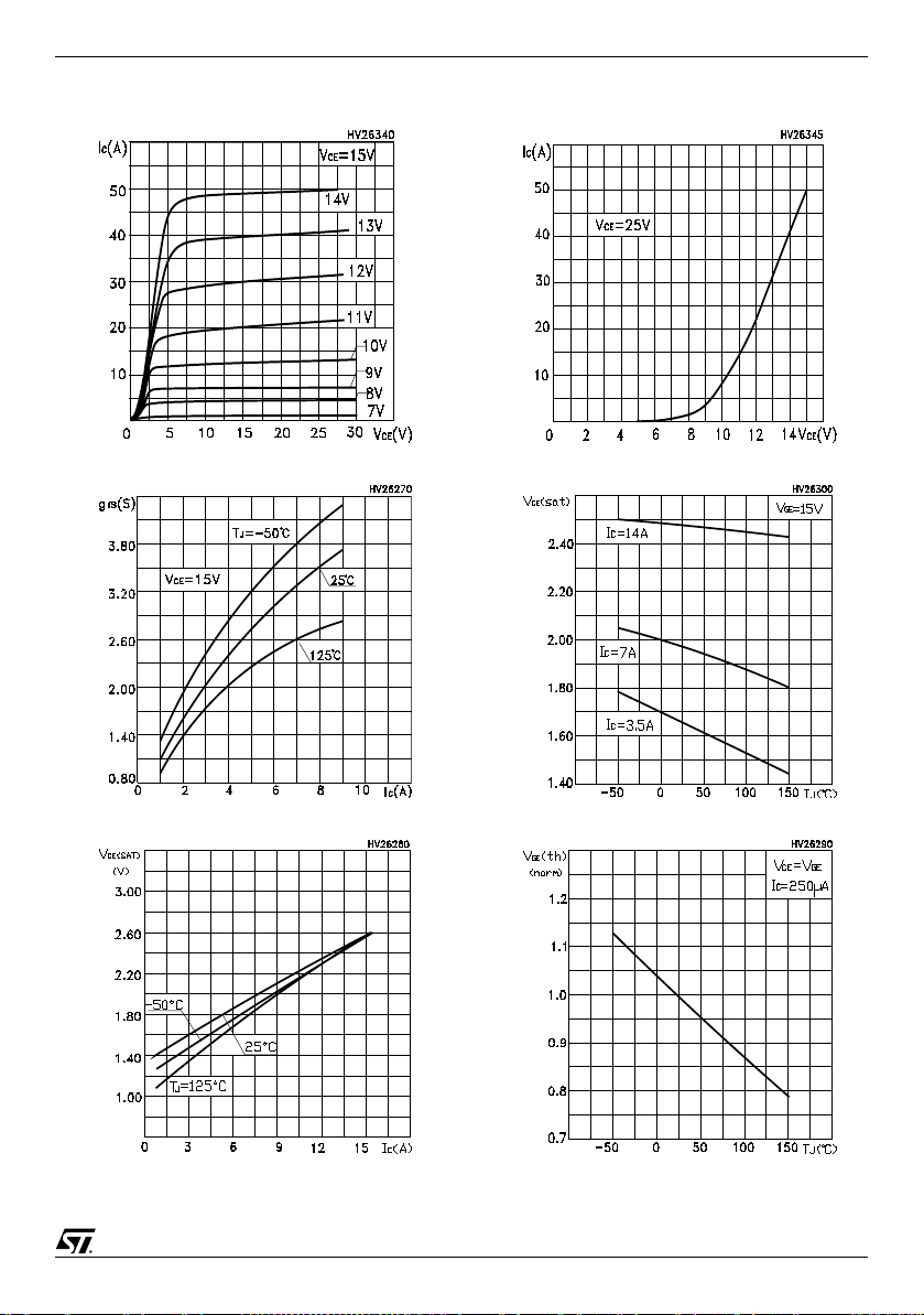
Figure 3: Output Characteristics
Figure 4: Transconductance
Figure 6: Transf er Characterist ics
Figure 7: Collector-Emitter On Voltage vs Temperature
Figure 5: Collector-Emitter On Voltage vs Collector Current
Figure 8 : Nor malize d G ate T hresh old v s Te mperature
5/14
 Loading...