

Features
■ Distortion-free negative signal throughput
down to V
■ Wide operating voltage range:
V
(opr) = 1.65 to 4.5 V single supply
CC
■ Ultra low power dissipation:
I
= 0.2 µA (max.) at TA = 85 °C
CC
■ Low ON resistance:
R
= 0.5 Ω (max. TA = 25 °C) at VCC = 3.6 V
ON
■ 4.3 V tolerant and 1.8 V compatible threshold
on digital control input at V
■ Latch-up performance exceeds 300 mA
(JESD 17)
■ ESD performance:
– 2000-V human-body model
(IEC61340-3-1:2002 level 2)
– 200-V machine model
(IEC61340-3-2 level M2)
– 1000-V charge device model
(JESD22-C101-A level III)
- 5.5 V
CC
= 1.65 V to 4.5 V
CC
STG5678
Low voltage dual SPDT switch
with negative rail capability
Flip-chip 12
Description
The STG5678 is a high-speed CMOS low voltage
dual analog SPDT (single pole dual throw) switch
or 2:1 multiplexer/de-multiplexer switch fabricated
in silicon gate CMOS technology. It is designed to
operate from 1.65 to 4.5 V.
The device is capable of handling signals with
negative voltages from V
any distortion.
- 5.5 V to VCC without
CC
Additional key features are fast switching speed,
break-before-make delay time and ultra low power
consumption. All inputs and outputs are equipped
with protection circuits against static discharge,
giving them ESD immunity and transient excess
voltage.
Table 1. Device summary
Order code Package Packaging
STG5678BJR Flip-chip 12 Tape and reel
STG5678CJR Flip-chip 12 (with back side coating) Tape and reel
June 2010 Doc ID 14580 Rev 3 1/23
www.st.com
23

Contents STG5678
Contents
1 Pin settings . . . . . . . . . . . . . . . . . . . . . . . . . . . . . . . . . . . . . . . . . . . . . . . . 3
1.1 Pin connection . . . . . . . . . . . . . . . . . . . . . . . . . . . . . . . . . . . . . . . . . . . . . . 3
1.2 Pin description . . . . . . . . . . . . . . . . . . . . . . . . . . . . . . . . . . . . . . . . . . . . . . 3
2 STG5678 device summary . . . . . . . . . . . . . . . . . . . . . . . . . . . . . . . . . . . . 4
3 Maximum rating . . . . . . . . . . . . . . . . . . . . . . . . . . . . . . . . . . . . . . . . . . . . . 5
3.1 Recommended operating conditions . . . . . . . . . . . . . . . . . . . . . . . . . . . . . 6
4 Electrical characteristics . . . . . . . . . . . . . . . . . . . . . . . . . . . . . . . . . . . . . 7
5 Test circuit . . . . . . . . . . . . . . . . . . . . . . . . . . . . . . . . . . . . . . . . . . . . . . . . 11
6 Application hint . . . . . . . . . . . . . . . . . . . . . . . . . . . . . . . . . . . . . . . . . . . . 15
6.1 Input signal dynamic range . . . . . . . . . . . . . . . . . . . . . . . . . . . . . . . . . . . 15
7 Package mechanical data . . . . . . . . . . . . . . . . . . . . . . . . . . . . . . . . . . . . 16
8 Revision history . . . . . . . . . . . . . . . . . . . . . . . . . . . . . . . . . . . . . . . . . . . 22
2/23 Doc ID 14580 Rev 3
STG5678 Pin settings
1 Pin settings
1.1 Pin connection
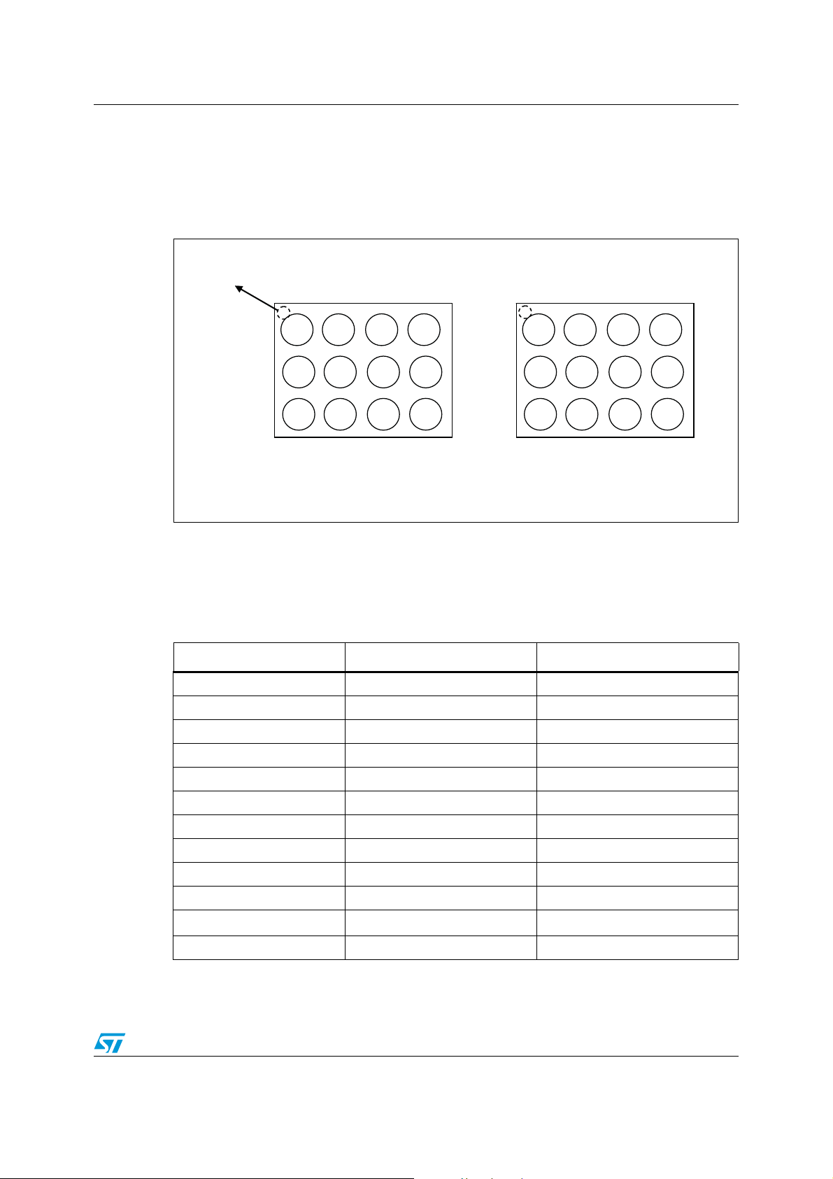
Figure 1. Pin connection (bump side view)
See note 1
1. Note 1: bump A1 is distinguished by a circular dot on the top-side. There is no circular dot on the bumpside.
A B C D
A1
A2
2
A3
1.2 Pin description
Table 2. Pin assignment
Pin number Symbol Name and function
B1
B2
B3
C1
C2
C3
D1
D2
D3
A B C D
1SEL
NC
2
2SEL
1S1
GND
2S1
D1
GND
D2
1S2
V
2S2
CC
A1 1SEL Selection control for switch 1
A2 NC No connection
A3 2SEL Selection control for switch 2
B1 1S1 Independent channel for switch 1
B2 GND Ground (0 V)
B3 2S1 Independent channel for switch 2
C1 D1 Common channel for switch 1
C2 GND Ground (0 V)
C3 D2 Common channel for switch 2
D1 1S2 Independent channel for switch 1
D2
V
CC
Positive supply voltage
D3 2S2 Independent channel for switch 2
Doc ID 14580 Rev 3 3/23
STG5678 device summary STG5678
2 STG5678 device summary
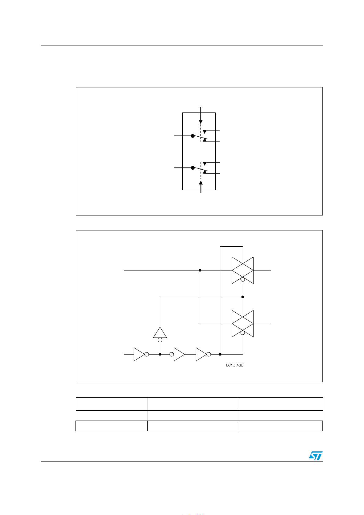
Figure 2. Functional diagram
D2
D2
D1
D1
Figure 3. Input equivalent circuit
D
2SEL
2SEL
1SEL
1SEL
2S1
2S1
2S2
2S2
1S1
1S1
1S2
1S2
S2
SEL
Table 3. Truth table
SEL Switch S1 Switch S2
HONOFF
LOFF
1. High impedance
4/23 Doc ID 14580 Rev 3
(1)
S1
(1)
ON
STG5678 Maximum rating
3 Maximum rating
Stressing the device above the rating listed in the “absolute maximum ratings” table may
cause permanent damage to the device. These are stress ratings only and operation of the
device at these or any other conditions above those indicated in the operating sections of
this specification is not implied. Exposure to absolute maximum rating conditions for
extended periods may affect device reliability.
Table 4. Absolute maximum ratings
Symbol Parameter Value Unit
V
V
V
I
I
I
I
CC
I
GND
P
T
1. Derate above 70 ºC by 18.5 mW/C
Supply voltage -0.5 to 5.5 V
CC
V
DC input voltage
I
DC control input voltage -0.5 to 5.5 V
IC
DC output voltage
O
DC input diode current on control pin (V
IKC
DC input diode current (VIN<0V) ±50 mA
I
IK
DC output diode current ±20 mA
OK
DC output current ±150 mA
I
O
DC output current peak (pulse at 1ms, 10% duty cycle) ±400 mA
OP
or
DC VCC or ground current ±100 mA
Power dissipation at TA = 70°C
D
Storage temperature -65 to 150 °C
stg
Lead temperature (10 sec) 300 °C
T
L
(1)
- 6.0) to
- (V
CC
VCC + 0.5
- 6.0 V) to
- (V
CC
+ 0.5
V
CC
<0V) -50 mA
SEL
1120 mW
V
V
Doc ID 14580 Rev 3 5/23
Maximum rating STG5678
3.1 Recommended operating conditions
Table 5. Recommended operating conditions
Symbol Parameter Value Unit
V
CC
V
I
V
IC
V
O
T
op
dt/dv
Supply voltage 1.65 to 4.5 V
Input voltage VCC -5.5 to V
CC
V
Control input voltage 0 to 4.5 V
Output voltage VCC -5.5 to V
CC
V
Operating temperature -40 to 85 °C
= 1.65 to 2.7 V 0 to 20
V
Input rise and fall time control
input
CC
= 3.0 to 4.5 V 0 to 10
V
CC
ns/V
6/23 Doc ID 14580 Rev 3
STG5678 Electrical characteristics
4 Electrical characteristics
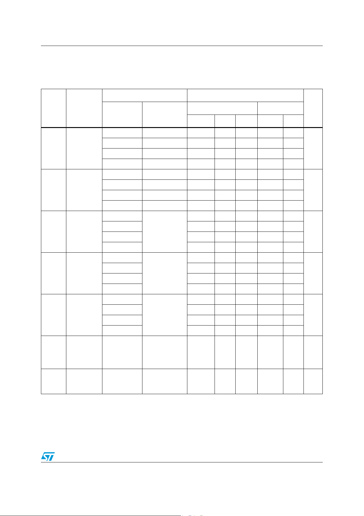
Table 6. DC specifications
Test conditions Value
Symbol Parameter
V
CC
(V)
1.65
−1.95 0.9 – – 0.9 –
2.25
V
IH
High level
input voltage
−2.7 0.9 – – 0.9 –
−4.3 1.0 – – 1.0 –
3.0
4.5 1.1 – – 1.1 –
1.65 −1.95 – – 0.6 – 0.6
2.25
V
IL
Low level
input voltage
−2.7 – – 0.6 – 0.6
3.0
−4.3 – – 0.7 – 0.7
4.5 – – 0.7 – 0.7
1.8
2.7 – 0.77 0.90 – 1.2
3.0 – 0.64 0.80 – 1.0
ON
Switch ON
resistance
R
3.6 – 0.51 0.65 – 1.0
1.8
2.7 – 20 – – 500
3.0 – 15 – – 500
3.6 – 15 – – 500
ΔR
ON
ON
resistance
match
between
channels
(1)
1.8
R
FLAT
ON
resistance
flatness
(2)
2.7 – 0.50 – – 0.8
3.0 – 0.40 – – 0.6
3.6 – 0.25 – – 0.5
Sn OFF
OFF
state
leakage
3.6
I
current
Sn ON state
I
ON
leakage
3.6
current
V
= V
S
CC
to VCC;
= 100 mA
I
S
at RON max
V
S
= 100 mA
I
S
V
= V
S
CC
to V
;
CC
= 100 mA
I
S
= -1.2 to
V
S
3.6 V
= 3.6 to
V
D
-1.2 V
= -1.2 to
V
S
3.6 V
= open
V
D
−5.5 V
−5.5 V
= 25 °C -40 to 85 °C
T
A
Min Typ Max Min Max
–3.804.60–7.0
– 50 – – 500
–3.5– –6.6
– -0.55 – -2 1 µA
– -0.55 – -2 1 µA
Unit
V
V
Ω
mΩ
Ω
Doc ID 14580 Rev 3 7/23
 Loading...