

Features
7AFER
■ High speed:
–t
= 130 ps (typ.) at VCC = 3.0 V
PD
–t
= 140 ps (typ.) at VCC = 2.3 V
PD
■ Ultra low power dissipation:
–I
= 0.2 μA (max.) at TA = 85 °C
CC
■ Low ON-resistance:
–R
–R
–R
■ Wide operating voltage range:
–V
■ 5 V tolerant and 1.8 V compatible threshold ON
digital control input at V
■ Latch-up performance exceeds 200 mA per
= 1.0 Ω (typ.) at VCC = 4.5 V
ON
= 1.2 Ω (typ.) at VCC = 3.0 V
ON
= 2.0 Ω (typ.) at VCC = 1.8 V
ON
(opr.) = 1.65 to 4.5 V single supply
CC
= 1.65 to 4.5 V
CC
JESD 78, Class II
■ ESD performance tested per JESD 22
– 2000 V human-body model
(A114-B, Class II)
– 200 V machine model (A115-A)
– 1000 V charged-device model (C101)
Description
The STG5123 is a high speed CMOS low voltage
single analog SPDT (single-pole double-throw)
switch or 2:1 multiplexer/demultiplexer switch
manufactured using silicon gate C
technology. Designed to operate from a 1.65 to
4.5 V supply, this device is ideal for portable
applications.
The device offers very low ON-resistance (1 Ω)
at V
= 4.5 V. Switch S1 is ON (connected to
CC
common ports Dn) when the SEL input is held
high, and OFF (state of high impedance exists
between the two ports) when SEL is held low.
2
MOS
STG5123
Low voltage 1 Ω single SPDT switch
with break-before-make feature
Datasheet − production data
DFN6L
Switch S2 is ON (connected to common port D)
when the SEL input is held low, and OFF (state
of high impedance exists between the two ports)
when SEL is held high.
Additional key features are fast switching speed,
break-before-make delay time and ultra low power
consumption. All inputs and outputs are equipped
with protection circuits to protect against static
discharge, giving them immunity from ESD and
transient excess voltage.
Table 1. Device summary
Order code Package Packaging
STG5123DTR
JSTG5123-CD1 Unsawn wafer
DFN6L
(1.2 x 1 mm)
Tape and reel
April 2012 Doc ID 14102 Rev 5 1/22
This is information on a product in full production.
www.st.com
1

Contents STG5123
Contents
1 Pin connections and functions . . . . . . . . . . . . . . . . . . . . . . . . . . . . . . . . 5
2 Electrical ratings . . . . . . . . . . . . . . . . . . . . . . . . . . . . . . . . . . . . . . . . . . . . 6
3 Electrical characteristics . . . . . . . . . . . . . . . . . . . . . . . . . . . . . . . . . . . . . 7
3.1 DC electrical characteristics . . . . . . . . . . . . . . . . . . . . . . . . . . . . . . . . . . . . 7
3.2 AC electrical characteristics . . . . . . . . . . . . . . . . . . . . . . . . . . . . . . . . . . . . 8
3.3 Analog switch characteristics . . . . . . . . . . . . . . . . . . . . . . . . . . . . . . . . . . . 9
4 Test circuits . . . . . . . . . . . . . . . . . . . . . . . . . . . . . . . . . . . . . . . . . . . . . . . 10
5 Package information . . . . . . . . . . . . . . . . . . . . . . . . . . . . . . . . . . . . . . . . 14
6 Die description . . . . . . . . . . . . . . . . . . . . . . . . . . . . . . . . . . . . . . . . . . . . 19
7 Revision history . . . . . . . . . . . . . . . . . . . . . . . . . . . . . . . . . . . . . . . . . . . 21
2/22 Doc ID 14102 Rev 5

STG5123 List of tables
List of tables
Table 1. Device summary. . . . . . . . . . . . . . . . . . . . . . . . . . . . . . . . . . . . . . . . . . . . . . . . . . . . . . . . . . 1
Table 2. Pin descriptions . . . . . . . . . . . . . . . . . . . . . . . . . . . . . . . . . . . . . . . . . . . . . . . . . . . . . . . . . . 5
Table 3. Truth table. . . . . . . . . . . . . . . . . . . . . . . . . . . . . . . . . . . . . . . . . . . . . . . . . . . . . . . . . . . . . . . 5
Table 4. Absolute maximum ratings . . . . . . . . . . . . . . . . . . . . . . . . . . . . . . . . . . . . . . . . . . . . . . . . . . 6
Table 5. Recommended operating conditions . . . . . . . . . . . . . . . . . . . . . . . . . . . . . . . . . . . . . . . . . . 6
Table 6. DC specifications . . . . . . . . . . . . . . . . . . . . . . . . . . . . . . . . . . . . . . . . . . . . . . . . . . . . . . . . . 7
Table 7. AC electrical characteristics (C
Table 8. Analog switch characteristics (C
Table 9. DFN6L (1.2 x 1 mm) mechanical data . . . . . . . . . . . . . . . . . . . . . . . . . . . . . . . . . . . . . . . . 15
Table 10. Pad information. . . . . . . . . . . . . . . . . . . . . . . . . . . . . . . . . . . . . . . . . . . . . . . . . . . . . . . . . . 20
Table 11. Document revision history . . . . . . . . . . . . . . . . . . . . . . . . . . . . . . . . . . . . . . . . . . . . . . . . . 21
= 35 pF, RL = 50 Ω, tr = tf ≤ 5 ns). . . . . . . . . . . . . . . . . . . . 8
L
= 5 pF, RL = 50 Ω, TA = 25 °C) . . . . . . . . . . . . . . . . . . . . 9
L
Doc ID 14102 Rev 5 3/22

List of figures STG5123
List of figures
Figure 1. Pin connections (top through view). . . . . . . . . . . . . . . . . . . . . . . . . . . . . . . . . . . . . . . . . . . . 5
Figure 2. Input equivalent circuit . . . . . . . . . . . . . . . . . . . . . . . . . . . . . . . . . . . . . . . . . . . . . . . . . . . . . 5
Figure 3. ON-resistance. . . . . . . . . . . . . . . . . . . . . . . . . . . . . . . . . . . . . . . . . . . . . . . . . . . . . . . . . . . 10
Figure 4. Bandwidth. . . . . . . . . . . . . . . . . . . . . . . . . . . . . . . . . . . . . . . . . . . . . . . . . . . . . . . . . . . . . . 10
Figure 5. OFF leakage . . . . . . . . . . . . . . . . . . . . . . . . . . . . . . . . . . . . . . . . . . . . . . . . . . . . . . . . . . . . 11
Figure 6. Channel-to-channel crosstalk . . . . . . . . . . . . . . . . . . . . . . . . . . . . . . . . . . . . . . . . . . . . . . . 11
Figure 7. OFF isolation . . . . . . . . . . . . . . . . . . . . . . . . . . . . . . . . . . . . . . . . . . . . . . . . . . . . . . . . . . . 12
Figure 8. Test circuit . . . . . . . . . . . . . . . . . . . . . . . . . . . . . . . . . . . . . . . . . . . . . . . . . . . . . . . . . . . . . 12
Figure 9. Break-before-make time delay . . . . . . . . . . . . . . . . . . . . . . . . . . . . . . . . . . . . . . . . . . . . . . 13
Figure 10. Switching time and charge injection
(V
= 0 V, R
Figure 11. Turn-on, turn-off delay time . . . . . . . . . . . . . . . . . . . . . . . . . . . . . . . . . . . . . . . . . . . . . . . . 13
Figure 12. DFN6L (1.2 x 1 mm) package outline . . . . . . . . . . . . . . . . . . . . . . . . . . . . . . . . . . . . . . . . . 14
Figure 13. DFN6L (1.2 x 1 mm) footprint recommendation . . . . . . . . . . . . . . . . . . . . . . . . . . . . . . . . . 15
Figure 14. DFN6L carrier tape information . . . . . . . . . . . . . . . . . . . . . . . . . . . . . . . . . . . . . . . . . . . . . 16
Figure 15. DFN6L reel information drawing (back view) . . . . . . . . . . . . . . . . . . . . . . . . . . . . . . . . . . . 17
Figure 16. DFN6L reel information drawing (front view) . . . . . . . . . . . . . . . . . . . . . . . . . . . . . . . . . . . 18
Figure 17. JSTG5123-CD1 die plot . . . . . . . . . . . . . . . . . . . . . . . . . . . . . . . . . . . . . . . . . . . . . . . . . . . 19
GEN
= 0 Ω, RL = 1 MΩ, CL = 100 pF) . . . . . . . . . . . . . . . . . . . . . . . . . . . . . . 13
GEN
4/22 Doc ID 14102 Rev 5
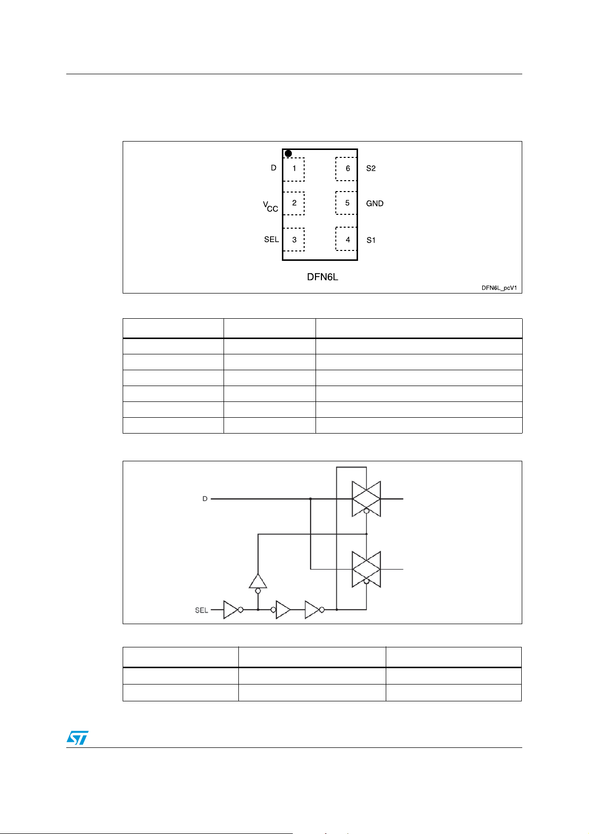
STG5123 Pin connections and functions
1 Pin connections and functions
Figure 1. Pin connections (top through view)
Table 2. Pin descriptions
Pin number Symbol Name and function
4 S1 Independent channel
6 S2 Independent channel
1 D Common channels
3 SEL Control
2V
CC
5 GND Ground (0 V)
Positive supply voltage
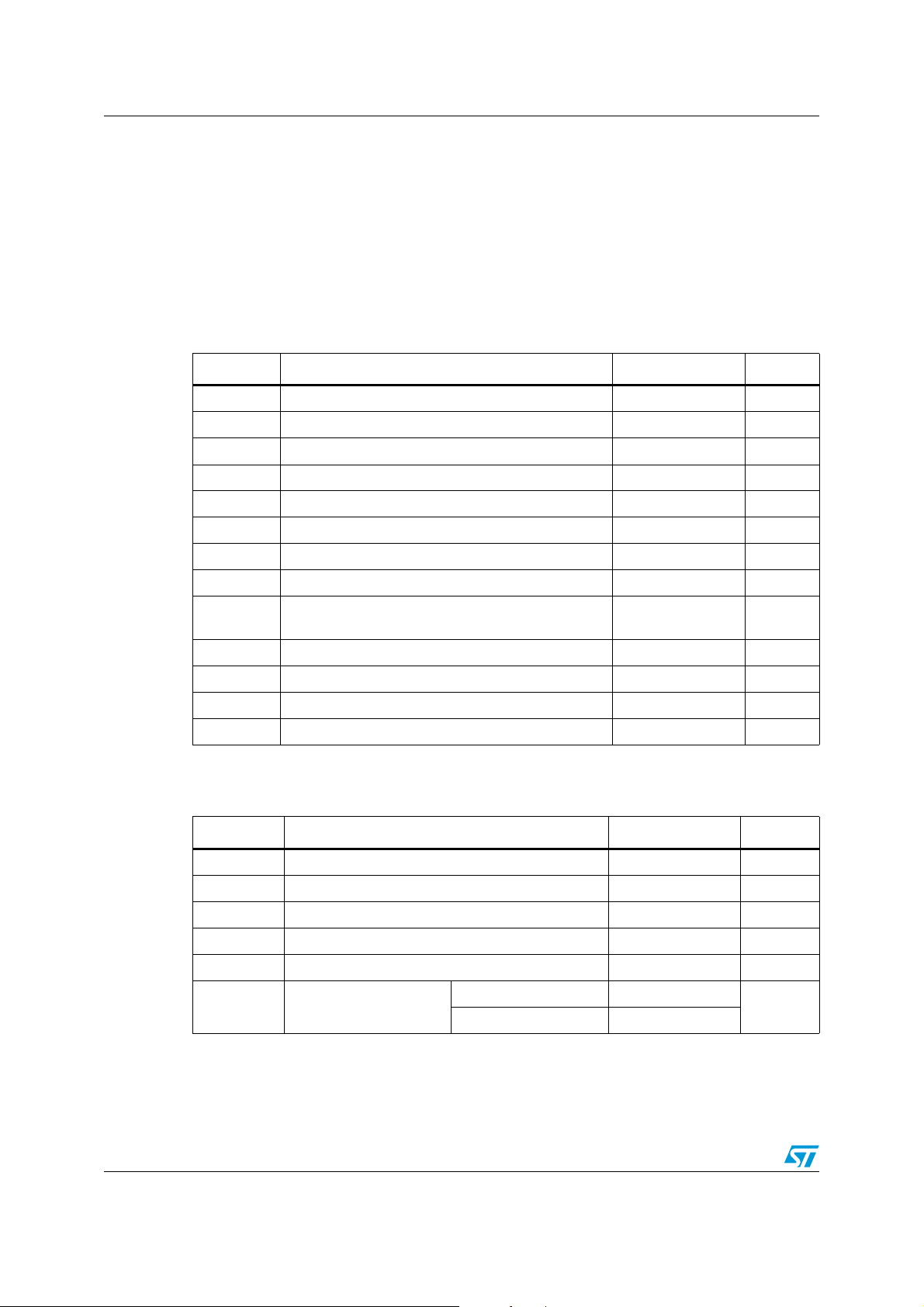
Figure 2. Input equivalent circuit
Table 3. Truth table
Sel Switch S1 Switch S2
HONOFF
LOFF
1. High impedance.
Doc ID 14102 Rev 5 5/22
(1)
S2
S1
(1)
ON
Electrical ratings STG5123
2 Electrical ratings
Stressing the device above the rating listed in Table 4: Absolute maximum ratings may
cause permanent damage to the device. These are stress ratings only and operation of the
device at these or any other conditions above those indicated in Table 5: Recommended
operating conditions of this specification is not implied. Exposure to absolute maximum
rating conditions for extended periods may affect device reliability. Refer also to the
STMicroelectronics™ SURE program and other relevant quality documents.
Table 4. Absolute maximum ratings
Symbol Parameter Value Unit
I
CC
V
V
V
V
I
IKC
I
I
OK
I
I
OP
or I
P
T
STG
T
CC
IC
O
IK
O
D
L
Supply voltage –0.5 to 5.5 V
DC input voltage –0.5 to V
I
CC
DC control input voltage –0.5 to 5.5 V
DC output voltage –0.5 to V
DC input diode current on control pin (V
DC input diode current (V
< 0 V) ±50 mA
IN
< 0 V) –50 mA
SEL
CC
DC output diode current ±20 mA
DC output current ±200 mA
DC output current peak
(pulse at 1 ms, 10% duty cycle)
DC VCC or ground current ±100 mA
GND
Power dissipation at TA = 70 °C
(1)
±400 mA
1120 mW
Storage temperature –65 to 150 °C
Lead temperature (10 s) 300 °C
+0.5 V
+0.5 V
1. Derate above 70 °C by 18.5 mW/°C.
Table 5. Recommended operating conditions
Symbol Parameter Value Unit
V
CC
V
V
IC
V
O
T
op
dt/dv
I
Supply voltage 1.65 to 4.5 V
Input voltage 0 to V
Control input voltage 0 to 4.5 V
Output voltage 0 to V
Operating temperature –40 to 85 °C
V
= 1.65 to 2.7 V 0 to 20
Input rise and fall time
control input
CC
V
= 3.0 to 4.5 V 0 to 10
CC
6/22 Doc ID 14102 Rev 5
CC
CC
V
V
ns/V
STG5123 Electrical characteristics
3 Electrical characteristics
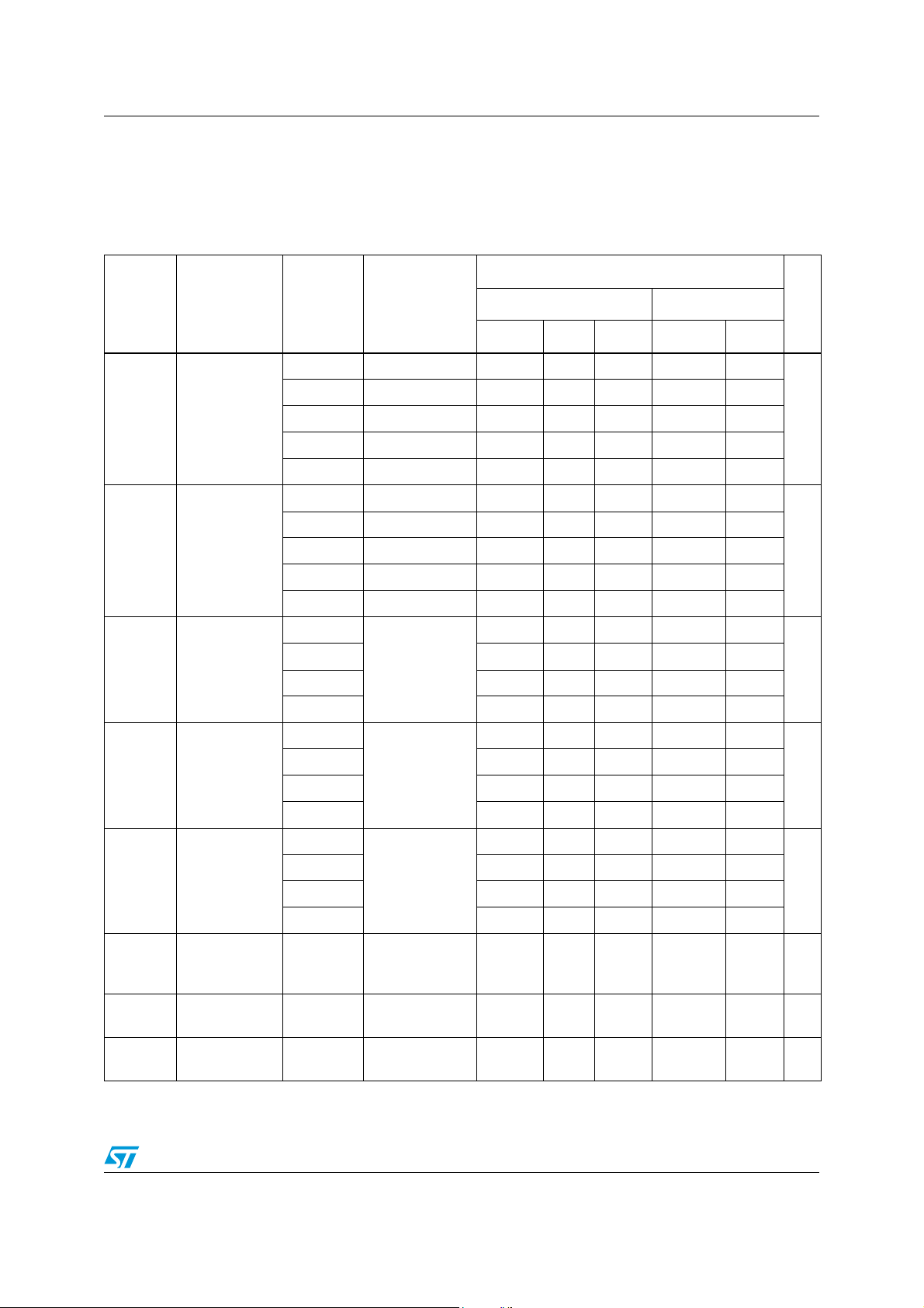
3.1 DC electrical characteristics
Table 6. DC specifications
Value
Symbol Parameter V
1.65 – 1.95 0.65 V
2.3 – 2.5 1.2 1.2
V
High level input
IH
voltage
2.7 – 3.0 1.3 1.3
3.3 – 3.6 1.4 1.4
1.65 – 1.95 0.40 0.40
2.3 – 2.5 0.60 0.60
IL
Low level input
voltage
2.7 – 3.0 0.60 0.60
V
3.3 – 3.6 0.60 0.60
ON
Switch ONresistance
R
ON-resistance
ΔR
match between
ON
channels
(1)
(V) Test condition
CC
Min. Typ. Max. Min. Max.
CC
0.65 V
CC
4.5 1.6 1.6
4.5 0.80 0.80
1.8
2.7 1.3 1.6 1.8
3.0 1.2 1.5 1.7
V
= 0 V to V
S
IS = 100 mA
CC
2.0 3.0 3.5
4.5 1.0 1.2 1.4
1.8
2.7 0.05
3.0 0.05
V
at RON max
S
= 100 mA
I
S
0.06
4.5 0.05
1.8
1.0 1.5 1.5
UnitTA = 25 °C -40 to 85 °C
V
V
Ω
Ω
R
FLAT
I
OFF
I
I
CC
IN
ON-resistance
flatness
(2)
OFF state
leakage current
(Sn), (D)
Input leakage
current
Quiescent
supply current
2.7 0.45 0.60 0.70
3.0 0.43 0.50 0.60
= 0 V to V
V
S
IS = 100 mA
CC
4.5 0.39 0.50 0.60
4.3 V
0 – 4.5 V
1.65 – 4.5
= 0.3 or 4 V ±20 ±100 nA
S
= 0 to 4.5 V ±0.1 ±1.0 μA
SEL
V
= VCC or
SEL
GND
±0.1 ±1.0 μA
Doc ID 14102 Rev 5 7/22
Ω
 Loading...