

ST STG3682 User Manual
查询STG3682QTR供应商
Low voltage high bandwidth dual SPDT switch
Features
■ Ultra low power dissipation:
–I
= 0.2µA (Max.) at TA = 85°C
CC
■ Low “ON” resistance:
–R
–R
■ Wide operating voltage range:
–V
■ 4.3V tolerant and 1.8V compatible threshold on
digital control input at V
■ Typical bandwidth (-3dB) at 800MHz on all
channels
■ Latch-up performance exceeds 100mA per
JESD 78, Class II
■ ESD performance exceeds JESD22
– 2000-V Human body model (A114-A)
■ USB (2.0) High speed (480Mbps) signal
switching compliant
= 4.6Ω (TA = 25°C) at VCC = 4.3V
ON
= 5.8Ω (TA = 25°C) at VCC = 3.0V
ON
(Opr) = 1.65V to 4.3V single supply
CC
= 2.3V to 3.0V
CC
STG3682
QFN10 (1.8mm x 1.4mm)
Description
The STG3682 is a high-speed CMOS low voltage
dual analog S.P.D.T. (Single Pole Dual Throw)
Switch or 2:1 Multiplexer /Demultiplexer Switch
fabricated in silicon gate C
designed to operate from 1.65V to 4.3V, making
this device ideal for portable applications.
The nSEL inputs are provided to control the
switch. The switch S1 is ON (they are connected
to common Ports Dn) when the nSEL input is held
high and OFF (high impedance state exists
between the two ports) when SEL is held low; the
switch S2 is ON (it is connected to common Port
D) when the nSEL input is held low and OFF (high
impedance state exists between the two ports)
when nSEL is held high.
2
MOS technology. It is
Additional key features are fast switching speed,
Break Before Make Delay Time and Ultra Low
Power Consumption. All inputs and outputs are
equipped with protection circuits against static
discharge, giving them ESD immunity and
transient excess voltage.
Order codes
Part number Package Packaging
STG3682QTR QFN10 (1.8mm x 1.4mm) Tape and reel
December 2006 Rev 1 1/19
www.st.com
19

Contents STG3682
Contents
1 Pin settings . . . . . . . . . . . . . . . . . . . . . . . . . . . . . . . . . . . . . . . . . . . . . . . . 3
1.1 Pin connection . . . . . . . . . . . . . . . . . . . . . . . . . . . . . . . . . . . . . . . . . . . . . . 3
1.2 Pin description . . . . . . . . . . . . . . . . . . . . . . . . . . . . . . . . . . . . . . . . . . . . . . 3
2 Device summary . . . . . . . . . . . . . . . . . . . . . . . . . . . . . . . . . . . . . . . . . . . . 4
3 Maximum rating . . . . . . . . . . . . . . . . . . . . . . . . . . . . . . . . . . . . . . . . . . . . . 5
3.1 Recommended operating conditions . . . . . . . . . . . . . . . . . . . . . . . . . . . . . 5
4 Electrical characteristics . . . . . . . . . . . . . . . . . . . . . . . . . . . . . . . . . . . . . 6
5 Test circuits . . . . . . . . . . . . . . . . . . . . . . . . . . . . . . . . . . . . . . . . . . . . . . 10
6 Package mechanical data . . . . . . . . . . . . . . . . . . . . . . . . . . . . . . . . . . . . 13
7 Revision history . . . . . . . . . . . . . . . . . . . . . . . . . . . . . . . . . . . . . . . . . . . 18
2/19
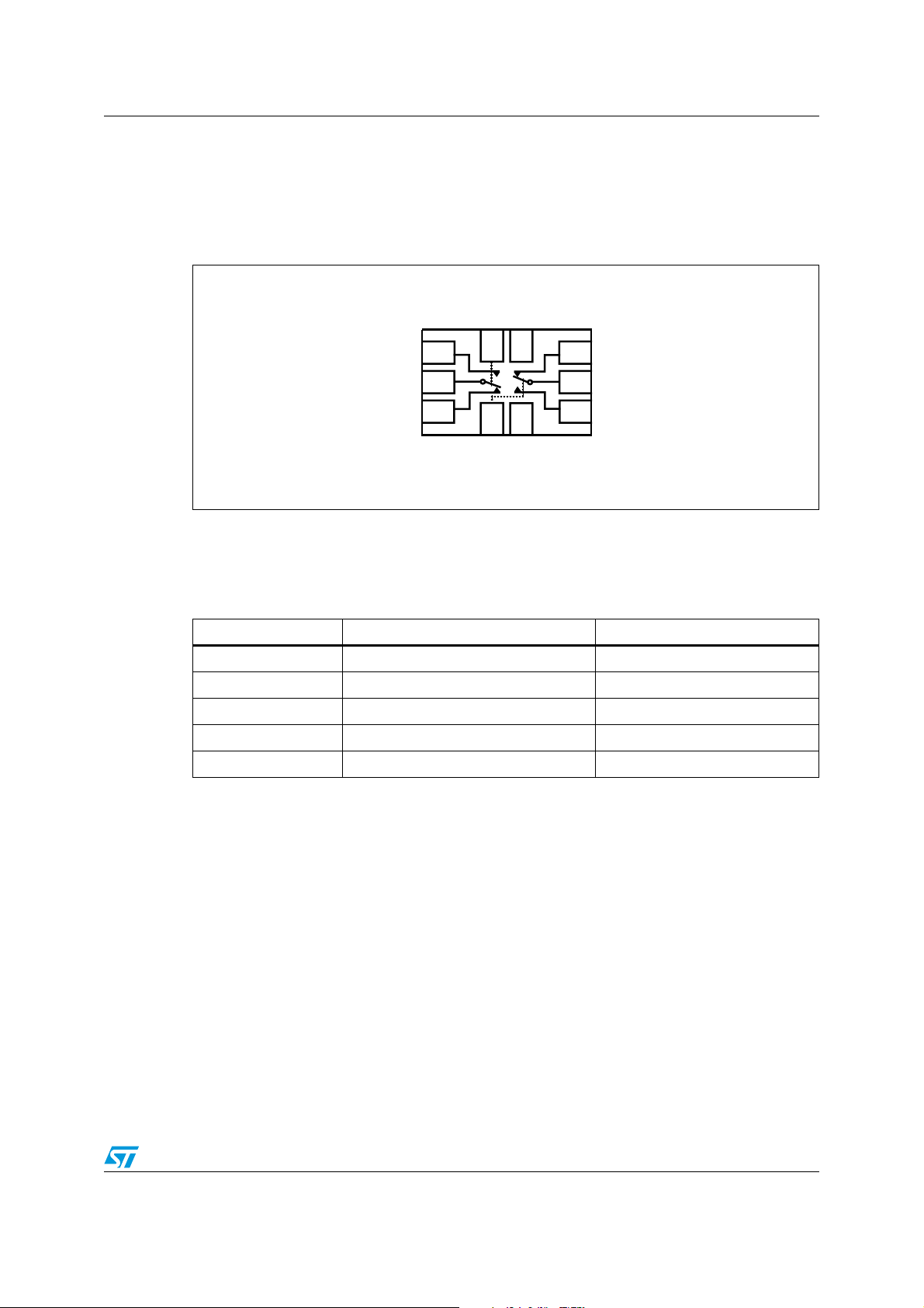
STG3682 Pin settings
1 Pin settings
1.1 Pin connection
Figure 1. Pin connection (top through view)
CC
V
SEL1
10
11S1
9
2S2
8
D1
1S2
2
3
54
GND
SEL2
D2
7
6
2S1
1.2 Pin description
Table 1. Pin description
Pin N° Symbol Name and function
1,3,6,8 1S1, 1S2, 2S1, 2S2 Independent channels
2,7 D1,D2 Common channels
10,4 SEL1,SEL2 Control
9 VCC Possitive supply voltage
5 GND Ground (0V)
Note: Exposed pad must be soldered to a floating plane. Do NOT connect to power or ground.
3/19
Device summary STG3682
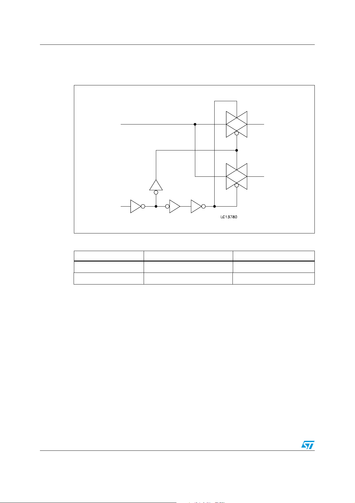
2 Device summary
Figure 2. Input equivalent circuit
D
SEL
Table 2. Truth table
SEL Switch S1 Switch S2
HON
L
1. High Impedance
OFF
(1)
S2
OFF
ON
S1
(1)
4/19
STG3682 Maximum rating
3 Maximum rating
Stressing the device above the rating listed in the “Absolute Maximum Ratings” table may
cause permanent damage to the device. These are stress ratings only and operation of the
device at these or any other conditions above those indicated in the Operating sections of
this specification is not implied. Exposure to Absolute Maximum Rating conditions for
extended periods may affect device reliability. Refer also to the STMicroelectronics SURE
Program and other relevant quality documents.
Table 3. Absolute maximum ratings
Symbol Parameter Value Unit
V
V
I
I
I
I
CC
I
GND
T
1. Derate above 70ºC by 18.5mW/C
Supply voltage -0.5 to 5.5 V
CC
V
DC input voltage
I
DC control input voltage -0.5 to 5.5 V
IC
V
DC output voltage
O
DC input diode current on control pin (V
IKC
I
DC input diode current (V
IK
DC output diode current ±20 mA
OK
I
DC output current ±128 mA
O
DC output current peak (pulse at 1ms, 10% duty cycle) ±300 mA
OP
or
DC VCC or ground current
P
Power dissipation at TA = 70°C
D
Storage temperature -65 to 150 °C
stg
T
Lead temperature (10 sec) 300 °C
L
SEL
<0V)
(1)
SEL
<0V)
-0.5 to V
-0.5 to V
CC
CC
-50 mA
±50 mA
±100 mA
1120 mW
+ 0.5
+ 0.5
V
V
3.1 Recommended operating conditions
Table 4. Recommended operating conditions
Symbol Parameter Value Unit
V
CC
Supply voltage
V
Input voltage 0 to V
I
V
V
T
dt/dv
1. Truth Table guaranteed: 1.2V to 4.3V
Control input voltage 0 to 4.3 V
IC
Output voltage 0 to V
O
Operating temperature -40 to 85 °C
op
Input rise and fall time control
input
(1)
V
= 1.65V to 2.7V
CC
V
= 3.0 to 4.3V
CC
5/19
1.65 to 4.3 V
CC
CC
0 to 20
ns/V
0 to 10
V
V
Electrical characteristics STG3682
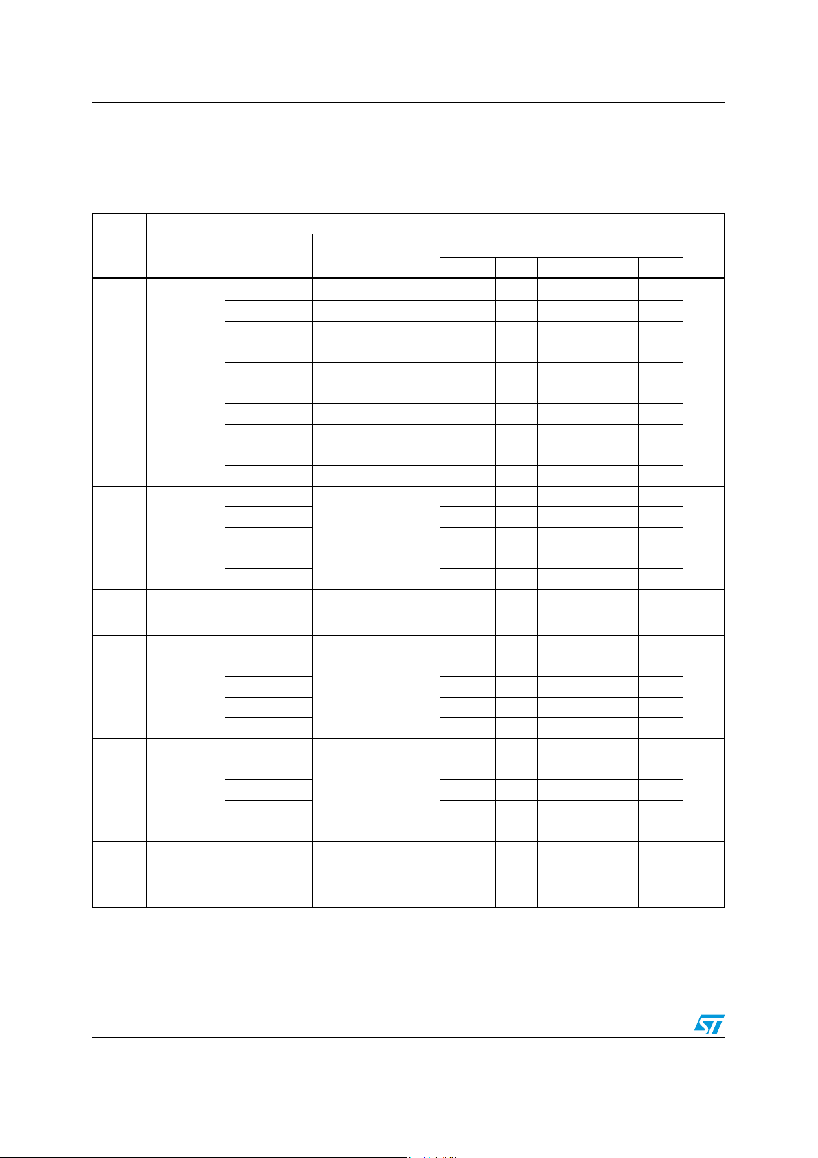
4 Electrical characteristics
Table 5. DC specifications
Test conditions Value
T
Symbol Parameter
High level
V
IH
input voltage
Low level
V
IL
input voltage
Switch ON
R
PEAK
peak
resistance
ON
Switch On
resistance
R
ON
resistance
ON
match
∆R
between
channels
(1)
ON
FLAT
resistance
flatness
(2)
R
OFF state
OFF
leakage
current
I
(SN), (D)
Vcc (V)
1.65 -1.95
0.65V
2.3-2.5 1.2 1.2
2.7-3.0 1.3 1.3
3.3-3.6 1.4 1.4
4.3 1.6 1.6
1.65-1.95 0.25
2.3-2.5 0.25
2.7-3.0 0.25
3.3-3.6 0.30
4.3 0.40
1.8
2.7 6.3 8.0
3.0 5.8 7.5
= 0V to V
V
S
IS = 8mA
CC
3.7 5.0 6.5
4.3 4.6 6.0
= 3V IS = 8mA
3.0
3.0
V
S
= 0.8V IS = 8mA
V
S
1.8
2.7
3.0 0.3
3.7
@ RON Max
V
S
= 8mA
I
S
4.3
1.8
2.7 2.0
3.0 1.7
= 0V to V
V
S
IS = 8mA
CC
3.7 1.5
4.3 1.6
= 0.3 or 4V
4.3
V
S
= 25°C
A
-40 to 85°C
Min Typ Max Min Max
CC
0.65V
CC
12.0 16.0
4.0 5.2
5.0 6.5
6.6
±20 ±100 nA
Unit
V
V
Ω
Ω
Ω
Ω
6/19
 Loading...