

ST STG3220 User Manual
Low voltage high bandwidth dual SPDT switch
Features
■ Ultra low power dissipation:
–I
= 1 μA (max.) at TA = 85 °C
CC
■ Low "ON" resistance:
–R
–R
■ Wide operating voltage range:
–V
■ 4.3 V tolerant and 1.8 V compatible threshold
on digital control input at V
■ Typical bandwidth (-3 dB) at 800 MHz on all
channels
■ USB (2.0) high speed (480 Mbps) signal
switching compliant
■ Integrated fail safe function
■ Interrupt function to indicate to the processor
that the device is in dedicated port charging
mode
■ Latch-up performance exceeds 500 mA per
JESD 78, Class II
■ ESD performance exceeds JESD22:
– Dn pins: 4000-V human body model
– All other pins: 2000-V human body model
Applications
■ Mobile phones
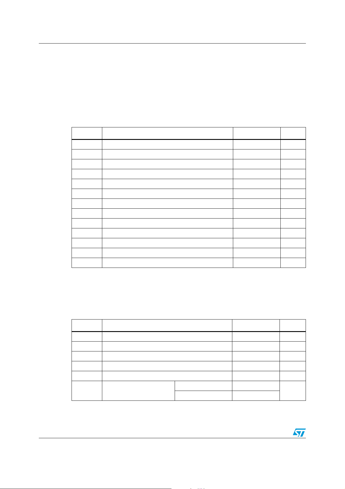
Table 1. Device summary
= 4.8 Ω (TA = 25 ºC) at VCC = 4.3 V
ON
= 5.9 Ω (TA = 25 ºC) at VCC = 3.0 V
ON
(opr) = 1.65 V to 4.3 V
CC
= 2.3 V to 3.0 V
CC
(A114-A)
(A114-A)
STG3220
QFN10
(1.8 x 1.4 mm)
Description
The STG3220 is a high-speed CMOS low voltage
dual analog SPDT (single pole dual throw) switch
or 2:1 multiplexer/de-multiplexer switch fabricated
in silicon gate C
to operate from 1.65 V to 4.3 V, making this
device ideal for portable applications.
The SEL input is provided to control the switch.
The switch nS1 is ON (connected to common
ports Dn) when the SEL input is held high and
OFF (high impedance state exists between the
two ports) when SEL is held low; the switch nS2 is
ON (it is connected to common port Dn) when the
SEL input is held low and OFF (high impedance
state exists between the two ports) when SEL is
held high. STG3220 has an integrated fail safe
function to withstand over-voltage condition when
the device is powered off.
The STG3220 also has an interrupt pin which
sends a signal to the processor when the device
is in dedicated port charging mode. Additional key
features are fast switching speed, break-beforemake-delay time and ultra low power
consumption. All inputs and outputs are equipped
with protection circuits against static discharge,
giving them ESD immunity and transient excess
voltage.
2
MOS technology. It is designed
Order code Package Packaging
STG3220QTR QFN10 (1.8 x 1.4 mm) Tape and reel
May 2009 Doc ID 15647 Rev 1 1/23
www.st.com
23

Contents STG3220
Contents
1 Pin settings . . . . . . . . . . . . . . . . . . . . . . . . . . . . . . . . . . . . . . . . . . . . . . . . 3
2 Logic diagram . . . . . . . . . . . . . . . . . . . . . . . . . . . . . . . . . . . . . . . . . . . . . . 4
3 Dedicated port charging detection . . . . . . . . . . . . . . . . . . . . . . . . . . . . . 5
4 Maximum rating . . . . . . . . . . . . . . . . . . . . . . . . . . . . . . . . . . . . . . . . . . . . . 6
4.1 Recommended operating conditions . . . . . . . . . . . . . . . . . . . . . . . . . . . . . 6
5 Electrical characteristics . . . . . . . . . . . . . . . . . . . . . . . . . . . . . . . . . . . . . 7
6 Test circuit . . . . . . . . . . . . . . . . . . . . . . . . . . . . . . . . . . . . . . . . . . . . . . . . 12
7 Package mechanical data . . . . . . . . . . . . . . . . . . . . . . . . . . . . . . . . . . . . 17
8 Revision history . . . . . . . . . . . . . . . . . . . . . . . . . . . . . . . . . . . . . . . . . . . 22
2/23 Doc ID 15647 Rev 1
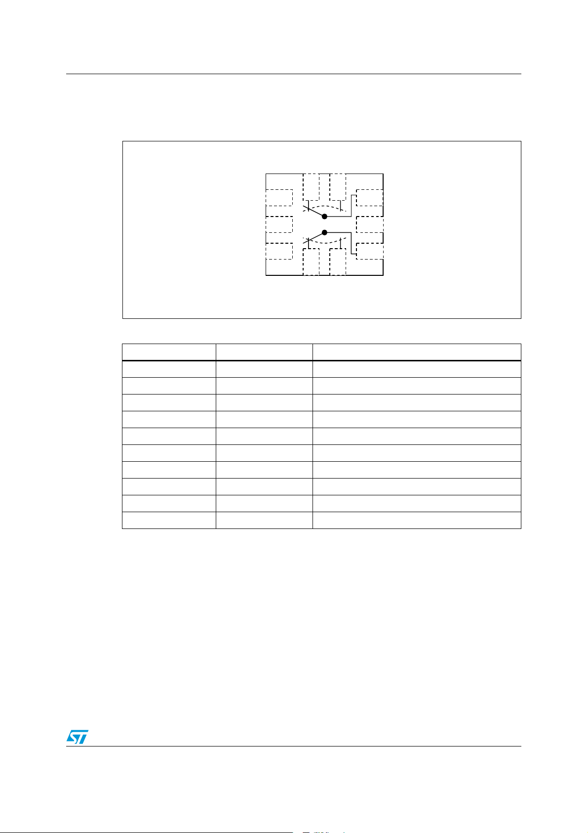
STG3220 Pin settings
4
3
1 Pin settings
Figure 1. Pin connection (top through view)
3
).
$
6##
3%,
'.$
$
3
Table 2. Pin description
Pin number Symbol Name and function
1 INT Interrupt
2 VCC Positive supply voltage
3 SEL Control
4 2S1 Independent channel for switch 2
5 2S2 Independent channel for switch 2
6 D2 Common channel for switch 2
7 GND Ground (0 V)
8 D1 Common channel for switch 1
9 1S2 Independent channel for switch 1
10 1S1 Independent channel for switch 1
Doc ID 15647 Rev 1 3/23
Logic diagram STG3220
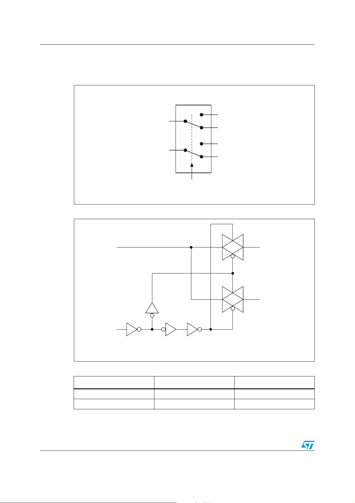
2 Logic diagram
Figure 2. Logic block diagram
1S1
D1
1S2
2S1
D2
2S2
SEL
Figure 3. Logic equivalent circuit
$N
N3
N3
3%,
!-6
Table 3. Truth table
SEL Switch nS1 Switch nS2
HONOFF
LOFF
(1)
1. High impedance.
(1)
ON
4/23 Doc ID 15647 Rev 1
STG3220 Dedicated port charging detection
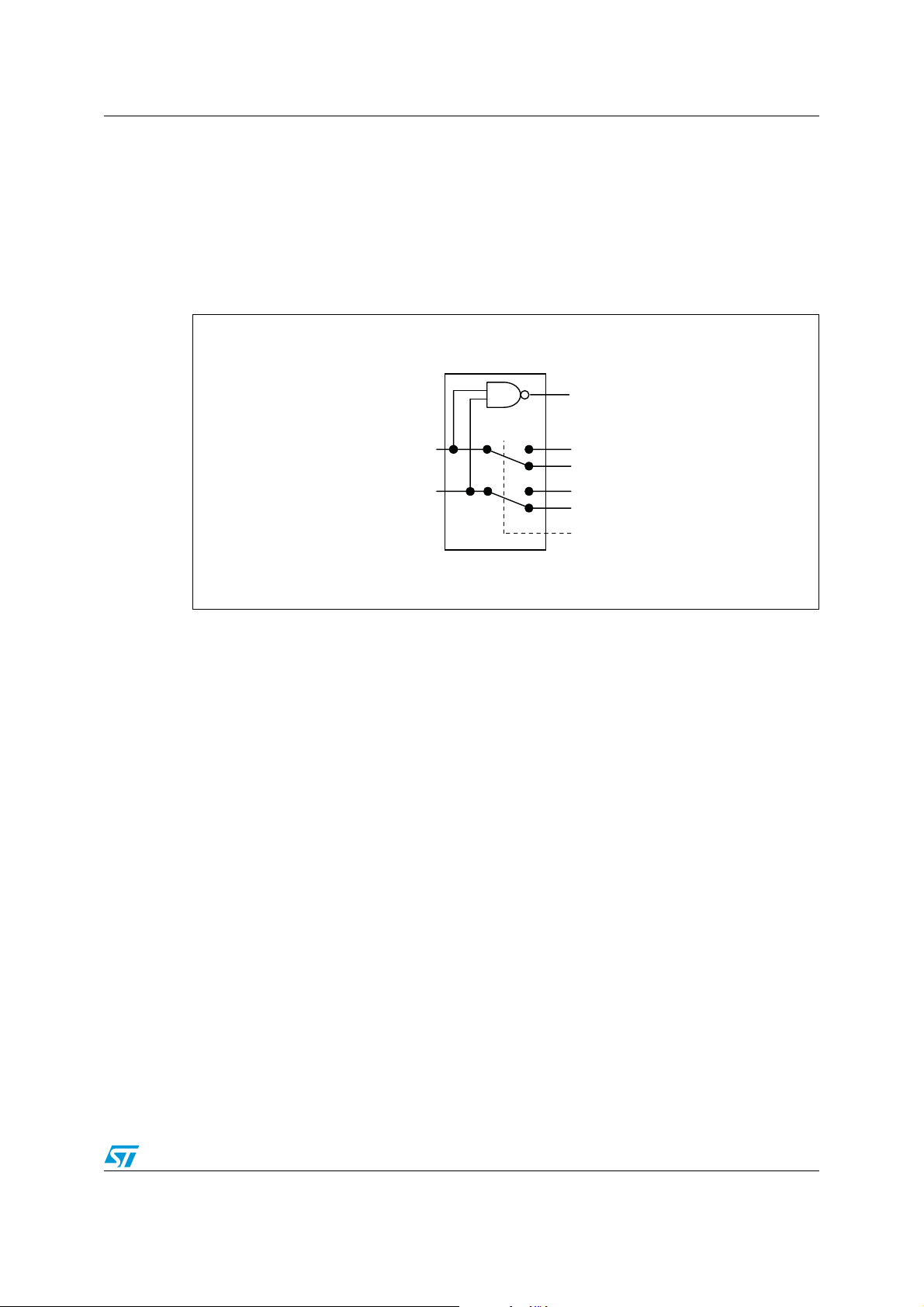
3 Dedicated port charging detection
The STG3220 has a built-in dedicated port charging detection circuit to detect the condition
when the USB D+/D- lines are both in high state. When this occurs, the device sends an
interrupt signal to the processor to indicate that the connected USB device is in dedicated
port charging mode.
Figure 4. Interrupt function logic representation
INT
D1
D2
1S1
1S2
2S1
2S2
SEL
Doc ID 15647 Rev 1 5/23
Maximum rating STG3220
4 Maximum rating
Stressing the device above the rating listed in the “Absolute maximum ratings” table may
cause permanent damage to the device. These are stress ratings only and operation of the
device at these or any other conditions above those indicated in the operating sections of
this specification is not implied. Exposure to absolute maximum rating conditions for
extended periods may affect device reliability.
Table 4. Absolute maximum ratings
Symbol Parameter Value Unit
V
CC
V
V
V
I
IKC
I
IK
I
OK
I
O
I
OP
or I
I
CC
P
T
stg
T
Supply voltage -0.5 to 5.5 V
DC input voltage -0.5 to VCC + 0.5 V
I
DC control input voltage -0.5 to 5.5 V
IC
DC output voltage -0.5 to VCC + 0.5 V
O
DC input diode current on control pin (V
DC input diode current (V
< 0V) ±50 mA
SEL
< 0V) -50 mA
SEL
DC output diode current ±20 mA
DC output current ±128 mA
DC output current peak (pulse at 1ms, 10% duty cycle) ±300 mA
DC VCC or ground current ±100 mA
GND
Power dissipation at TA = 70 °C
D
(1)
Storage temperature -65 to +150 °C
Lead temperature (10 sec) 300 °C
L
1. Derate above 70 °C by 18.5 mW/°C.
4.1 Recommended operating conditions
Table 5. Recommended operating conditions
1120 mW
Symbol Parameter Value Unit
V
CC
V
V
V
T
op
dt/dv
Supply voltage 1.65 to 4.3 V
Input voltage 0 to V
I
Control input voltage 0 to 4.3 V
IC
Output voltage 0 to V
O
Operating temperature -40 to 85 °C
Input rise and fall time control
input
6/23 Doc ID 15647 Rev 1
= 1.65 V to 2.7 V 0 to 20
V
L
= 3.0 to 4.3 V 0 to 10
V
L
CC
CC
V
V
ns/V
STG3220 Electrical characteristics
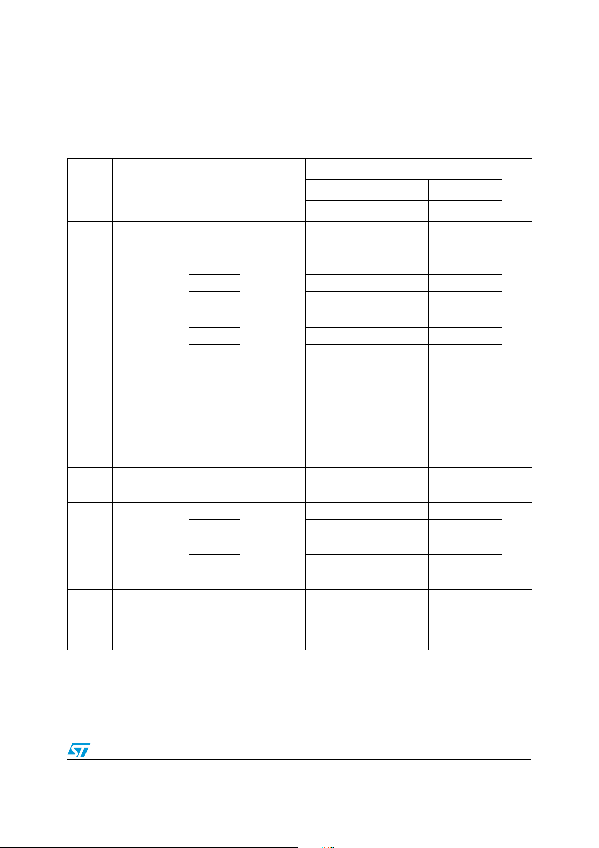
5 Electrical characteristics
Table 6. DC specifications
Val ue
Symbol Parameter
V
(V)
CC
Test
conditions
= 25 °C -40 to 85 °C
A
Min Typ Max Min Max
UnitT
V
V
V
IH-INT
V
IL-INT
V
OL-INT
High level input
IH
voltage
Low level input
IL
voltage
High level input
voltage for INT
Low level input
voltage for INT
Low level output
voltage for INT
1.65 – 1.95
0.65 V
CC
––0.65VCC–
2.3 – 2.5 1.2 – – 1.2 –
2.7 – 3.0 1.3 – – 1.3 –
–
3.3 – 3.6 1.4 – – 1.4 –
4.3 1.6 – – 1.6 –
1.65 – 1.95
– – 0.25 – 0.25
2.3 – 2.5 – – 0.25 – 0.25
2.7 – 3.0 – – 0.25 – 0.25
–
3.3 – 3.6 – – 0.30 – 0.30
4.3 – – 0.40 – 0.40
4.3 – 2.4 – – 2.4 – V
4.3 – – – 0.9 – 0.9 V
4.3 I
1.8
= 4 mA – – 0.40 – 0.50 V
O
– 15.1 17.8 – –
V
V
R
PEAK
Switch ON peak
resistance
2.7 – 6.4 8.0 – –
3.0 – 5.9 7.5 – –
3.7 – 5.0 6.5 – –
= 0 V to
V
S
V
CC
= 8 mA
I
S
Ω
4.3 – 4.8 6.1 – –
= 3 V
V
3.0
ON
Switch ON
resistance
R
3.0
S
I
= 8 mA
S
= 0.4 V
V
S
IS = 8 mA
–4.25.4––
Ω
–5.77.0––
Doc ID 15647 Rev 1 7/23
 Loading...